Die attach for light emitting diode
US20050006755A1
2005-01-13
10/617,626
2003-07-10
✅ Patent granted
US 7,075,233 B2
2006-07-11
-
-
Joseph Williams
2024-05-25
Abstract:
Improved LED die mount. By mounting an LED die on a pedestal which is smaller than the LED die, formation of fillets of die mount material which would block some of the light from the LED die are reduced or eliminated.
Inventors:
- Kee Yean Ng 77 🇲🇾 Penang, Malaysia
- Teong Heng Sim 2 🇲🇾 Penang, Malaysia
- Chong Hai Lee 2 🇲🇾 Penang, Malaysia
Interested in similar patents?
Get notified when new applications in this technology area are published.
Classification:
H01L33/62 » CPC main
Semiconductor devices with at least one potential-jump barrier or surface barrier specially adapted for light emission; Processes or apparatus specially adapted for the manufacture or treatment thereof or of parts thereof; Details thereof characterised by the semiconductor body packages Arrangements for conducting electric current to or from the semiconductor body, e.g. lead-frames, wire-bonds or solder balls
H01L24/32 » CPC further
Arrangements for connecting or disconnecting semiconductor or solid-state bodies; Methods or apparatus related thereto; Means for bonding being attached to, or being formed on, the surface to be connected, e.g. chip-to-package, die-attach, "first-level" interconnects; Manufacturing methods related thereto; Layer connectors, e.g. plate connectors, solder or adhesive layers; Manufacturing methods related thereto; Structure, shape, material or disposition of the layer connectors after the connecting process of an individual layer connector
H01L24/83 » CPC further
Arrangements for connecting or disconnecting semiconductor or solid-state bodies; Methods or apparatus related thereto; Methods for connecting semiconductor or other solid state bodies using means for bonding being attached to, or being formed on, the surface to be connected using a layer connector
H01L33/20 » CPC further
Semiconductor devices with at least one potential-jump barrier or surface barrier specially adapted for light emission; Processes or apparatus specially adapted for the manufacture or treatment thereof or of parts thereof; Details thereof characterised by the semiconductor bodies with a particular shape, e.g. curved or truncated substrate
H01L2224/83385 » CPC further
Indexing scheme for arrangements for connecting or disconnecting semiconductor or solid-state bodies and methods related thereto as covered by; Methods for connecting semiconductor or other solid state bodies using means for bonding being attached to, or being formed on, the surface to be connected using a layer connector; Bonding interfaces outside the semiconductor or solid-state body Shape, e.g. interlocking features
H01L2924/01322 » CPC further
Indexing scheme for arrangements or methods for connecting or disconnecting semiconductor or solid-state bodies as covered by; Alloys; Binary Alloys Eutectic Alloys, i.e. obtained by a liquid transforming into two solid phases
H01L2924/15153 » CPC further
Indexing scheme for arrangements or methods for connecting or disconnecting semiconductor or solid-state bodies as covered by; Details of package parts other than the semiconductor or other solid state devices to be connected; Die mounting substrate; Shape the die mounting substrate comprising a recess for hosting the device
H01L2924/12036 » CPC further
Indexing scheme for arrangements or methods for connecting or disconnecting semiconductor or solid-state bodies as covered by; Details of semiconductor or other solid state devices to be connected; Device type; Passive devices, e.g. 2 terminal devices; Rectifying Diode PN diode
H01L2924/12041 » CPC further
Indexing scheme for arrangements or methods for connecting or disconnecting semiconductor or solid-state bodies as covered by; Details of semiconductor or other solid state devices to be connected; Device type; Passive devices, e.g. 2 terminal devices; Optical Diode LED
H01L2924/00 » CPC further
Indexing scheme for arrangements or methods for connecting or disconnecting semiconductor or solid-state bodies as covered by
H05B33/00 IPC
Electroluminescent light sources
Description
BACKGROUND OF THE INVENTION1. Field of the Invention
The present invention relates to the field of Light Emitting Diodes (LEDs). More particularly, it pertains to a method of attaching the LED die to improve light output.
2. Art Background
In use, Light Emitting Diode (LED) dies are packaged by mounting them to a substrate such as a printed circuit board (PCB) or a leadframe. The LED die is mounted to the substrate using a material such as an adhesive, often epoxy-based conductive adhesives, solder, solder paste, or eutectic alloys. When the die is mounted, the mounting material naturally forms a fillet up the side walls of the LED die. Being opaque, the fillet blocks a portion of the light generated by the LED.
SUMMARY OF THE INVENTIONBy mounting the LED die on a pedestal smaller than the die, fillets formed by die attach material along the sides of the die are reduced or eliminated.
BRIEF DESCRIPTION OF THE DRAWINGSThe present invention is described with respect to particular exemplary embodiments thereof and reference is made to the drawings in which:
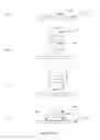
FIG. 1 shows an LED die mount,
FIG. 2 shows an LED die mount according to the present invention,
FIG. 3 shows an additional LED die mount according to the present invention, and
FIG. 4 shows an additional embodiment of the present invention.
DETAILED DESCRIPTIONFIG. 1 shows a LED die mounted according to the prior art. Detail A shows die mount material 100 on substrate 110. While the substrate shown in FIG. 1 is flat, it may be curved, such as a curved mount used for single LEDs. The die mount material may be an adhesive such as a conductive epoxy, or may be solder, solder paste, or a eutectic alloy as known to the art.
Detail B shows collet 130 supporting LED die 140. Collet 130 may be operated automatically or by hand. Detail C shows the collet and die moving to contact the substrate and die mount material.
Detail D shows LED die 140 affixed to substrate 110, with fillets 150 of the die mount material flowing along the sides of LED 140. The opaque nature of fillets 150 blocks light ray 160. This is a particular problem if the active PN junction of die 140 is near substrate 110 and subject to being blocked by fillets 150.
According to one embodiment of the present invention as shown in FIG. 2, Detail A shows die mount material 200 placed on pedestal 220 on substrate 210. Pedestal 220 is smaller in size than the LED die to be attached. Pedestal 220 may be formed through the stamping process in the case where substrate 210 is a leadframe. Pedestal 220 may be formed through a plating process in the case where substrate 210 is a printed circuit board (PCB). Pedestal 220 may also be a separate component attached to substrate 210. The height of pedestal 220 is determined mainly by the characteristics of die mount material 200. The shape of pedestal 220 does not have to match that of die 240. For example, both die 240 and pedestal 220 may be rectangular in shape. In other instances, die 240 may be square or rectangular, and pedestal 220 may be circular or oval.
Detail B shows collet 230 supporting LED die 240. Detail C shows the collet and die moving to contact the die mount material on the pedestal and substrate.
Detail D shows LED die 240 affixed to pedestal 220 and substrate 210. Since pedestal 220 is smaller than die 240, fillets 250 of mount material do not encroach on the sides of LED die 240. Thus, light ray 260 is not blocked.
It is also possible to first affix the pedestal to the die, and then affix the combined pedestal and pedestal to the substrate.
FIG. 3 shows an embodiment of the present invention in which the substrate is curved, as in a leadframe. In this embodiment, leadframe 310 is formed with raised pedestal 320 to which LED die 340 is attached. As pedestal 320 is smaller than LED die 340, fillets 350 of die attach material do not obscure the sides of LED die 340, this allowing light ray 360 to pass. Also shown in FIG. 3, the sides of pedestal 320 do not have to be normal to the substrate, or parallel to each other.
FIG. 4 shows an additional embodiment of the invention in which pedestal 420 is formed as part of die 440. The pedestal feature may be formed by mechanical means such as sawing, or by chemical means such as dry or wet etching.
The foregoing detailed description of the present invention is provided for the purpose of illustration and is not intended to be exhaustive or to limit the invention to the precise embodiments disclosed. Accordingly the scope of the present invention is defined by the appended claims.
Claims
1. An improved light emitting diode mount comprising:
a light emitting diode die,
a substrate, and
a pedestal smaller than the die connecting the die to the substrate.
2. The device of claim 1 where the pedestal is formed as part of the die.
3. The device of claim 1 where the pedestal is formed as part of the substrate.
4. The device of claim 1 where the pedestal is a separate component from the substrate and the die.
5. The method of mounting a light emitting diode die to a substrate comprising:
Forming a pedestal smaller than the die on one surface of the die, and
affixing the pedestal to the substrate.
6. The method of mounting a light emitting diode die to a substrate comprising:
Forming a pedestal smaller than the die on the substrate, and
affixing the die to the pedestal.
7. The method of mounting a light emitting diode die to a substrate comprising:
Affixing a pedestal smaller than the die to the substrate, and
affixing the die to the pedestal.
8. The method of mounting a light emitting diode die to a substrate comprising:
Affixing a pedestal smaller than the die to the die, and
affixing the pedestal to the substrate.
Images & Drawings included:


Sources:
- United States Patent and Trademark Office - verify current appl. status at the USPTO↗
Similar patent applications:
- » 20120193649
Light emitting diode (LED) arrays including direct die attach and related assemblies - » 20120305949
Light emitting diode (LED) arrays including direct die attach and related assemblies - » 20130193453
Light emitting diode (LED) arrays including direct die attach and related assemblies - » 20110031502
Light emitting diodes including integrated backside reflector and die attach - » 20160149104
Light emitting diode (LED) components including LED dies that are directly attached to lead frames - » 20170155026
Light emitting diode (LED) components including multiple LED dies that are attached to lead frames
Recent applications in this class:
- » 20250072195 2025-02-27
ELECTRONIC DEVICE - » 20250072194 2025-02-27
LIGHT-EMITTING ELEMENT AND METHOD OF PRODUCING LIGHT-EMITTING ELEMENT - » 20250072193 2025-02-27
DISPLAY DEVICE - » 20250072192 2025-02-27
SEMICONDUCTOR DEVICE - » 20250072191 2025-02-27
LED DRIVING DEVICE, METHOD OF FABRICATING LED DRIVING DEVICE AND DISPLAY DEVICE INCLUDING LED DRIVING DEVICE - » 20250072190 2025-02-27
ELECTRONIC DEVICE - » 20250072189 2025-02-27
DISPLAY PANEL - » 20250072188 2025-02-27
DISPLAY DEVICE - » 20250072187 2025-02-27
OPTOELECTRONIC ARRAY AND METHOD FOR MANUFACTURING AN OPTOELECTRONIC ARRAY - » 20250072186 2025-02-27
MULTILAYER STRUCTURE, PACKAGE COMPONENT AND OPTICAL SEMICONDUCTOR DEVICE