Micro lead frame package having transparent encapsulant
US20050146057A1
2005-07-07
10/869,981
2004-06-17
Abstract:
The present invention discloses an MLP having an optically transparent encapsulant. The MLP comprises a lead frame having a die-pad, a plurality of lead fingers and an interlock undercut. A die is placed onto the die-pad. A conductive wire is provided for connecting the die to the plurality of lead finger. The package is then encapsulated using optically transparent encapsulant.
Inventors:
- Ah Lek Khor 2 🇲🇾 Ipoh, Malaysia
- Kock Huat Lee 2 🇲🇾 Ipoh, Malaysia
- Boon Meng Chan 2 🇲🇾 Ipoh, Malaysia
- Min Kong Thum 2 🇲🇾 Menglembu, Malaysia
- Hong Mun Tung 2 🇲🇾 Ipoh, Malaysia
- Mun Tuck Cheong 2 🇲🇾 Ipoh, Malaysia
Interested in similar patents?
Get notified when new applications in this technology area are published.
Classification:
H01L23/49548 » CPC main
Details of semiconductor or other solid state devices; Arrangements for conducting electric current to or from the solid state body in operation, e.g. leads, terminal arrangements ; Selection of materials therefor consisting of soldered constructions; Lead-frames or other flat leads; Geometry of the lead-frame Cross section geometry
H01L23/3107 » CPC further
Details of semiconductor or other solid state devices; Encapsulations, e.g. encapsulating layers, coatings, e.g. for protection characterised by the arrangement or shape the device being completely enclosed
H01L24/97 » CPC further
Arrangements for connecting or disconnecting semiconductor or solid-state bodies; Methods or apparatus related thereto; Batch processes at chip-level, i.e. with connecting carried out on a plurality of singulated devices, i.e. on diced chips the devices being connected to a common substrate, e.g. interposer, said common substrate being separable into individual assemblies after connecting
H01L27/14618 » CPC further
Devices consisting of a plurality of semiconductor or other solid-state components formed in or on a common substrate including semiconductor components sensitive to infra-red radiation, light, electromagnetic radiation of shorter wavelength or corpuscular radiation and specially adapted either for the conversion of the energy of such radiation into electrical energy or for the control of electrical energy by such radiation; Devices controlled by radiation; Imager structures; Structural or functional details thereof Containers
H01L24/48 » CPC further
Arrangements for connecting or disconnecting semiconductor or solid-state bodies; Methods or apparatus related thereto; Means for bonding being attached to, or being formed on, the surface to be connected, e.g. chip-to-package, die-attach, "first-level" interconnects; Manufacturing methods related thereto; Wire connectors; Manufacturing methods related thereto; Structure, shape, material or disposition of the wire connectors after the connecting process of an individual wire connector
H01L24/73 » CPC further
Arrangements for connecting or disconnecting semiconductor or solid-state bodies; Methods or apparatus related thereto Means for bonding being of different types provided for in two or more of groups , , , , , , ,
H01L2924/01005 » CPC further
Indexing scheme for arrangements or methods for connecting or disconnecting semiconductor or solid-state bodies as covered by; Chemical elements Boron [B]
H01L2924/01006 » CPC further
Indexing scheme for arrangements or methods for connecting or disconnecting semiconductor or solid-state bodies as covered by; Chemical elements Carbon [C]
H01L2924/01012 » CPC further
Indexing scheme for arrangements or methods for connecting or disconnecting semiconductor or solid-state bodies as covered by; Chemical elements Magnesium [Mg]
H01L2924/01019 » CPC further
Indexing scheme for arrangements or methods for connecting or disconnecting semiconductor or solid-state bodies as covered by; Chemical elements Potassium [K]
H01L2924/01029 » CPC further
Indexing scheme for arrangements or methods for connecting or disconnecting semiconductor or solid-state bodies as covered by; Chemical elements Copper [Cu]
H01L2924/01033 » CPC further
Indexing scheme for arrangements or methods for connecting or disconnecting semiconductor or solid-state bodies as covered by; Chemical elements Arsenic [As]
H01L2924/01078 » CPC further
Indexing scheme for arrangements or methods for connecting or disconnecting semiconductor or solid-state bodies as covered by; Chemical elements Platinum [Pt]
H01L2924/01079 » CPC further
Indexing scheme for arrangements or methods for connecting or disconnecting semiconductor or solid-state bodies as covered by; Chemical elements Gold [Au]
H01L2924/01082 » CPC further
Indexing scheme for arrangements or methods for connecting or disconnecting semiconductor or solid-state bodies as covered by; Chemical elements Lead [Pb]
H01L2924/16195 » CPC further
Indexing scheme for arrangements or methods for connecting or disconnecting semiconductor or solid-state bodies as covered by; Details of package parts other than the semiconductor or other solid state devices to be connected; Cap; Shape Flat cap [not enclosing an internal cavity]
H01L2224/85 » CPC further
Indexing scheme for arrangements for connecting or disconnecting semiconductor or solid-state bodies and methods related thereto as covered by; Methods for connecting semiconductor or other solid state bodies using means for bonding being attached to, or being formed on, the surface to be connected using a wire connector
H01L2224/83 » CPC further
Indexing scheme for arrangements for connecting or disconnecting semiconductor or solid-state bodies and methods related thereto as covered by; Methods for connecting semiconductor or other solid state bodies using means for bonding being attached to, or being formed on, the surface to be connected using a layer connector
H01L2224/97 » CPC further
Indexing scheme for arrangements for connecting or disconnecting semiconductor or solid-state bodies and methods related thereto as covered by; Batch processes at chip-level, i.e. with connecting carried out on a plurality of singulated devices, i.e. on diced chips the devices being connected to a common substrate, e.g. interposer, said common substrate being separable into individual assemblies after connecting
H01L2224/73265 » CPC further
Indexing scheme for arrangements for connecting or disconnecting semiconductor or solid-state bodies and methods related thereto as covered by; Means for bonding being of different types provided for in two or more of groups; Location after the connecting process on different surfaces Layer and wire connectors
H01L2924/12042 » CPC further
Indexing scheme for arrangements or methods for connecting or disconnecting semiconductor or solid-state bodies as covered by; Details of semiconductor or other solid state devices to be connected; Device type; Passive devices, e.g. 2 terminal devices; Optical Diode LASER
H01L2924/181 » CPC further
Indexing scheme for arrangements or methods for connecting or disconnecting semiconductor or solid-state bodies as covered by; Details of package parts other than the semiconductor or other solid state devices to be connected Encapsulation
H01L2924/00012 » CPC further
Indexing scheme for arrangements or methods for connecting or disconnecting semiconductor or solid-state bodies as covered by; Technical content checked by a classifier Relevant to the scope of the group, the symbol of which is combined with the symbol of this group
H01L2924/14 » CPC further
Indexing scheme for arrangements or methods for connecting or disconnecting semiconductor or solid-state bodies as covered by; Details of semiconductor or other solid state devices to be connected; Device type Integrated circuits
H01L2924/00 » CPC further
Indexing scheme for arrangements or methods for connecting or disconnecting semiconductor or solid-state bodies as covered by
H01L2224/45099 » CPC further
Indexing scheme for arrangements for connecting or disconnecting semiconductor or solid-state bodies and methods related thereto as covered by; Means for bonding being attached to, or being formed on, the surface to be connected, e.g. chip-to-package, die-attach, "first-level" interconnects; Manufacturing methods related thereto; Wire connectors; Manufacturing methods related thereto; Structure, shape, material or disposition of the wire connectors prior to the connecting process of an individual wire connector; Core members of the connector Material
H01L2924/00014 » CPC further
Indexing scheme for arrangements or methods for connecting or disconnecting semiconductor or solid-state bodies as covered by; Technical content checked by a classifier the subject-matter covered by the group, the symbol of which is combined with the symbol of this group, being disclosed without further technical details
H01L2924/207 » CPC further
Indexing scheme for arrangements or methods for connecting or disconnecting semiconductor or solid-state bodies as covered by; Parameters Diameter ranges
Description
TECHNICAL FIELD OF THE INVENTIONThe present invention generally relates to a micro lead frame package (hereinafter called as MLP throughout the specification) especially to an MLP having a transparent encapsulant.
BACKGROUND OF THE INVENTIONIn recent years, there has been a strong demand for an MLP that has a low dielectric rate, high heat conductivity and a desired thermal expansion coefficient. Advantageously, the thermal expansion coefficient of the MLP is similar to that of the electronic parts having an extensive storing capability, a high-speed operation and a low fabrication cost. Further, there is a strong demand for MLP with light sensors to cater for increasing popularity of light sensitive or light activated instrument such as LASER diodes and other semiconductor devices that incorporate optical sensors.
To meet this demand, an MLP with a transparent window was developed. FIG. 1 shows a typical MLP with a transparent window of the prior art. It is a ceramic dual-in-line package (CERDIP) of a charge-coupled device (CCD). As shown therein, the MLP (1) comprises a die (11), a ceramic lower plate (12) which acts as a die pad, a lead frame (14), a ceramic upper plate (15) and a window (10). A die sealant (13) is applied to one side of a central portion of the die pad (12). The die (11) is then attached to the die pad (12) by placing it on the die sealant (13). Later, a ceramic sealant (16) is applied to top fringe of the die pad (12), mount a lead frame (14) thereon, apply a ceramic sealant (16) to the lead frame (14) and fixing the upper ceramic plate (15) onto the lead-frame (14). To complete the assembly, the die (11) and the lead frame (14) are electrically connected by a conductive wire (18), and a transparent window (10) is sealed by a transparent window sealant (17).
In a more detail, the ceramic package of the prior art is directed to applying a ceramic plate sealant (16) onto the top fringe of the die pad (12), and mounting the lead frame (14) thereon. In addition, the ceramic upper plate (15) of which the lower side is provided with the ceramic plate sealant (16) is mounted on the lead frame (14), and is then heat-treated, so that the ceramic plate sealant (16) is molten to seal the lead framed (14) to the ceramic upper plate (15).
Meanwhile, the die sealant (13) is applied to a central portion of the die pad (12), and the die (11) is mounted thereon, and is heat-treated. Thereafter, the die (11) and the inner lead (19) of the lead frame (14) are bonded using a wire (18). The transparent window (10) of which one side is provided with the transparent window sealant (17) is mounted on the ceramic upper plate (15). The transparent window sealant (17) is heat-treated to melting to sealingly attach the transparent window (10) to the upper portion of the ceramic upper plate (15).
After the above operation, the lead frame (14) is trimmed, and the fabrication of the ceramic MLP is completed. However, the ceramic MLP of the prior art and the fabrication method thereof have the following problems.
Firstly, to provide a ceramic sealant (16) coat on lower side of the ceramic upper plate (15) involves fabrication processes that are both intricate and complex that inevitably leads to high fabrication cost. Secondly, it is almost impossible to achieve a desired sealant effect between the ceramic upper plate (15) and the window sealant (17). This normally leads to damage where the window (10) peels off from the ceramic upper plate (15).
In another type of MLP (2) with transparent window as shown in FIG. 2, a die (21) is first placed on o die-pad (22) of the lead-frame (23). Connections (25) are then made between the die (21) and lead fingers (24) of the lead frame (23). A predetermined volume of transparent plastic (24) is then applied enough to cover the die (21) and the die-pad (22). Thereafter the package is moulded to form MLP with the clear transparent plastic forming a window.
This type of MLP is easier and thus less costly to manufacture and in many instances is more superior in term of performance and reliability compared to the previous example. However, some problems still persist with this type of MLP in that the transparent plastic normally have a different coefficient of expansion with the moulding compound resulting in disassociation of materials after some time of use. This disassociation will lead to crack that will damage the MLP.
In an effort to reduce the amount of moulding material and the process use for cost reduction and other apparent benefits, attempts have been made to mould one side of the lead-frame using a single compound, that is a transparent plastic. The results have been very encouraging, however, there is still a drawback in that the transparent plastic easily peels off from the lead-frame especially during cooling resulting in reject of the MLP. Therefore, there arises a need to provide a new design for MLP that lacks or at least minimises the above problems. This has become the main object of the present invention.
SUMMARY OF THE INVENTIONAccordingly, it is an object of the present invention to provide an MLP with a transparent encapsulation.
It is another object of the present invention to provide an MLP with a transparent encapsulation that is easy and cheap to employ.
It is yet another object of the present invention to provide an MLP with a transparent encapsulation that is both reliable and durable.
These and other object of the present invention are accomplished by,
A Micro Lead Frame Package (3), comprising:
a lead frame (31) having a die-pad (32), a plurality of lead fingers (53) and an interlock undercut (34);
-
- a die (35) placed onto said die-pad (32);
- conductive wire (36) connecting said die (35) to said plurality of lead finger (33); and
- an encapsulant (37),
- characterised by
- said encapsulant (37) being optically transparent.
Other aspect of the present innovation and their advantages will be discerned after studying the Detailed Description in conjunction with the accompanying drawings in which:
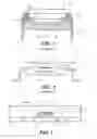
FIG. 1 showing a cross-sectional view of the ceramic MLP with transparent window of the prior art.
FIG. 2 showing a cross-sectional view of another prior art of ceramic MLP with transparent window.
FIG. 3 showing a cross-sectional view of the MLP with transparent encapsulant according to one embodiment of the present invention.
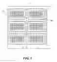
FIG. 4 showing a lead frame body with a plurality of lead frame arranged in a matrix-array.
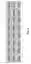
FIG. 5 showing a lead frame body with stress-relief means.
DETAILED DESCRIPTION OF THE DRAWINGSReferring now to FIG. 3 showing a cross-sectional view of the MLP with transparent encapsulant according to one embodiment of the present invention. The MLP (3) comprises a lead frame (31) having a die-pad (32) and a plurality of lead fingers (33). On the underside of the lead frame (31) an interlock undercut (34) is provided by shallowly machining away part of the lead frame (31) along the shank. A die (35) is placed and secured onto the die-pad (32) after which conductive wire (36) connecting the die (35) to a plurality of lead finger (33). The lead frame is then encapsulated by an optically transparent plastic encapsulant (37) to form the MLP. In MLP of the prior art encapsulation is carried out on both side of the lead frame. However, in the present invention encapsulation is carried out only to one side of the lead frame. This reduces material used, making the package smaller and lighter with other inherent advantages.
One of the major problems with one side encapsulation of MLP is delamination of the encapsulant. In the present invention, a sort of a locking means is provided to lock the encapsulant permanently to the lead frame. This is achieved through the interlock undercut (34) that is provided to the lead frame (31). During encapsulantion the heat will cause the encapsulant (37) to melt and flow into the interlock undercut (34) and on cooling the encapsulant will lock permanently to the lead frame (31) thus forming a locking means that eliminate delamination.
Referring now to FIG. 4 showing a Lead Frame body with a plurality of lead frame arranged in a matrix-array. The Lead Frame body (4) for fabrication of MLP, comprises a plurality of a lead frame (41) each having a die-pad (not shown), a plurality of lead fingers (not shown) and an interlock undercut. The lead frame (41) are arranged in matrix-array for convenience of fabrication. This arrangement may look simple but it has one inherent advantage never thought possible before, it allows the use of a single mould for fabrication of MLP of various sizes and shapes. This proves to be very attractive technically and economically.
Referring now to FIG. 5 showing a Lead Frame body with stress-relief means. One of the main problems in the fabrication of MLP is what is term as “delamination”, that the plastic encapsulant has a tendency of peeling off from the lead frame during cooling. This is caused by the different coefficient of expansion between the plastic encapsulant and the lead frame which results in different contraction of the materials. In the present invention, this problem is checked by using a stress relief means to check the propagation of the delamination. The Lead Frame body (51) being provided with a stress-relief means (52) in the form of slots in between one matrix to another matrix of lead frames. By doing this, should delamination occur to one matrix, it would not spread to other matrix thus saving other matrices from delamination.
While the preferred embodiment of the present invention and their advantages have been disclosed in the above Detailed Description, the invention is not limited thereto but only by the scope of the appended claims.
Claims
1. A Micro Lead Frame Package, comprising:
a lead frame having a die-pad, a plurality of lead fingers and an interlock undercut;
a die placed onto said die-pad;
conductive wire connecting said die to said plurality of lead finger; and
an encapsulant,
characterised by
said encapsulant being optically transparent.
2. A Micro Lead Frame Package as claimed in claim 1, further characterised by said encapsulant being applied to one side of said lead frame.
3. A Micro Lead Frame Package as claimed in claim 2, further characterised by said encapsulant flowing into said interlock undercut to form a locking means.
4. A Lead Frame body for fabrication of micro lead frame package, comprising:
a plurality of a lead frame each having a die-pad, a plurality of lead fingers and an interlock undercut;
characterised by
said plurality of lead frame being arranged in a matrix-array.
5. A Lead Frame body as claimed in claim 4, further characterised by said lead frame being provided with a stress-relief means.
6. A Lead Frame body as claimed in claim 4, further characterised by said stress-relief means being slots.
Images & Drawings included:

Sources:
- United States Patent and Trademark Office - verify current appl. status at the USPTO↗
Recent applications in this class:
- » 20250149413 2025-05-08
SEMICONDUCTOR DEVICE AND METHOD OF MANUFACTURING SEMICONDUCTOR DEVICE - » 20250140654 2025-05-01
PACKAGE CARRIER HAVING LARGE CORNER LEADS WITH LEAD TIP INSPECTION FEATURE - » 20250132232 2025-04-24
ELECTRONIC DEVICE - » 20250112131 2025-04-03
LEAD FRAME AND SEMICONDUCTOR DEVICE - » 20250105105 2025-03-27
SEMICONDUCTOR DEVICE - » 20250096080 2025-03-20
SEMICONDUCTOR DEVICE - » 20250079271 2025-03-06
SEMICONDUCTOR DEVICE, POWER CONVERTER, AND METHOD OF MANUFACTURING SEMICONDUCTOR DEVICE - » 20250079270 2025-03-06
Power Management Integrated Circuit (PMIC) and Power Management System - » 20250054842 2025-02-13
PACKAGE WITH CONCAVE WETTABILITY AND/OR METALLIZATION LAYER - » 20250022779 2025-01-16
SEMICONDUCTOR PACKAGE