Heating resistances and heaters
US20050173411A1
2005-08-11
11/024,244
2004-12-28
✅ Patent granted
US 7,332,694 B2
2008-02-19
-
-
Tu Ba Hoang | Stephen J. Ralis
2024-12-28
Abstract:
A heating resistance 1 comprises a shaped body of a band made of a conductive material obtained by bending the band in a shape of a wave. The heating resistance 1 is fixed to a substrate made of an insulating material to obtain a heater. Alternatively, the heating resistance comprises a wound body of a band made of a conductive material. According to the present invention, the heating value per a unit length can be easily designed and changed, and the reliability can be improved and abnormal heat generation can be prevented at the interface where the heating value per a unit length is changed.
Assignee:
- NGK Insulators, Ltd. 2,193 🇯🇵 Nagoya-City, Japan
- NGK INSULATORS, LTD. 2,607 🇯🇵 Nagoya, Japan
Interested in similar patents?
Get notified when new applications in this technology area are published.
Classification:
H05B3/143 » CPC main
Ohmic-resistance heating; Heater elements characterised by the composition or nature of the materials or by the arrangement of the conductor characterised by the composition or nature of the conductive material the material being non-metallic; Conductive ceramics, e.g. metal oxides, metal carbides, barium titanate, ferrites, zirconia, vitrous compounds applied to semiconductors, e.g. wafers heating
H05B3/748 » CPC further
Ohmic-resistance heating; Heating arrangements specially adapted for cooking plates or analogous hot-plates; Non-metallic plates, e.g. vitroceramic, ceramic or glassceramic hobs, also including power or control circuits Resistive heating elements, i.e. heating elements exposed to the air, e.g. coil wire heater
H01L21/67103 » CPC further
Processes or apparatus adapted for the manufacture or treatment of semiconductor or solid state devices or of parts thereof; Apparatus specially adapted for handling semiconductor or electric solid state devices during manufacture or treatment thereof; Apparatus specially adapted for handling wafers during manufacture or treatment of semiconductor or electric solid state devices or components ; Apparatus not specifically provided for elsewhere; Apparatus not specifically provided for elsewhere; Apparatus for manufacture or treatment; Apparatus for thermal treatment mainly by conduction
H05B3/18 IPC
Ohmic-resistance heating; Heater elements characterised by the composition or nature of the materials or by the arrangement of the conductor the conductor being embedded in an insulating material
H05B3/68 IPC
Ohmic-resistance heating Heating arrangements specially adapted for cooking plates or analogous hot-plates
H01C3/08 IPC
Non-adjustable metal resistors made of wire or ribbon, e.g. coiled, woven or formed as grids Dimension or characteristic of resistive element changing gradually or in discrete steps from one terminal to another
Description
This application claims the benefits of Japanese Patent Application P2004-1725 filed on Jan. 7, 2004, the entirety of which is incorporated by reference.
BACKGROUND OF THE INVENTION1. Field of the Invention
The invention relates to a heating resistance and heater suitable to, for example, heating semiconductors, whose temperature distribution can be easily controlled.
2. Related Art Statement
In a system for producing semiconductors, a ceramic heater has been applied for heating a wafer so as to deposit a semiconductor thin film on the wafer from gaseous raw materials such as silane gas by means of thermal CVD or the like. In such ceramic heater, it is required to make the temperature of the heating face and the semiconductor wafer mounted thereon uniform at a high precision.
It has been known several techniques for reducing temperature distribution on the heating (mounting) face of the ceramic heater. For example, so-called two-zone heater is known as such heater. Such two-zone heater has a ceramic substrate and inner and outer resistance heat generators embedded in the substrate. Separate power supply terminals are connected to the respective heat generators so that electric power may be applied independently on the respective generators. Heat generated from the inner and outer heat generators may be thus independently controlled.
Such type of two-zone heater includes the followings. Japanese patent publication 2001-102157A discloses a heater having a ceramic substrate and two layers of heating elements embedded in the substrate. The calorific values in the inner zone and outer zone of each heating element are controlled so that two-zone control system of inner and outer zones is realized.
It is desired to provide a design for adjusting heat generation density from a heating resistance embedded in a ceramic heater, depending on actual environmental conditions where the heater is set. For example, when a heating resistance (wound body) having a shape of coil spring is embedded in a ceramic substrate, the heat generation density per a unit area can be raised by increasing the winding number or winding diameter (coil diameter) or by reducing the wire diameter. Further, the heat generation density per a unit area can be lowered by reducing the winding number or winding diameter (coil diameter) or by increasing the wire diameter.
Normally, the material of a heating resistance embedded in a ceramic substrate should be a high melting point metal which does not melt and easily deform at the sintering temperature of a ceramics, and thus is limited. For example, when a wound body of a molybdenum wire or tungsten wire is used, it is difficult to change the winding diameter or wire diameter in a single wound body due to the limitation of manufacturing process. It is thus necessary that a plurality of wound bodies having the different winding diameters, winding numbers or wire diameters are joined and electrically connected with each other before the connected wound bodies are embedded in a ceramic substrate.
According to Japanese Patent publication 2003-272, 805A, for example, when a heating resistance composed of a tungsten coil is embedded in a ceramic substrate, two kinds of heating resistances having the different wire diameters and winding diameters are used and mechanically connected with each other using a spherical connecting terminal. It is thus possible to embed and combine two or more kinds of heating resistances having the different wire diameters or winding diameters in a single ceramic substrate so that hot and cold spots on the surface of the substrate can be reduced.
SUMMARY OF THE INVENTIONThe material of a heating resistance embedded in a ceramic substrate is, for example, a high melting point metal such as tungsten or molybdenum. A wire made of such high melting point metal is hard, brittle, hard to deform and thus difficult to process. The terminal described above is thus necessary for connecting a plurality of heating resistances having the different wire diameters. However, if the resistance at the connecting part of the heating resistance and the terminal in use is raised, hot spots may be observed on the heating face. Moreover, for assuring excellent mechanical strength and reliability of the connecting parts of the heating resistance and the terminal, the structure, shape and connecting method of the connecting part are needed to be studied in detail. The manufacturing process required for producing the connecting part may become troublesome.
An object of the present invention is, in a heating resistance, to make the design and change of the heating value per a unit length easier, and to improve the reliability and prevent abnormal heat generation at interface where the heating value per a unit length is changed.
A first aspect of the present invention provides a heating resistance comprising a shaped body of a band made of a conductive material, said shaped body comprises a shape of a wave. The first aspect of the present invention further provides a heater comprising a substrate made of an insulating material and the above heating resistance fixed to the substrate.
According to the first aspect, it is necessary that the shaped body has a shape of a wave in a front view as FIGS. 1(b), 2(b) or 9(b). The wave shape is not particularly limited as far as the shaped body has repetition units each composed of wall parts in a front view. The wave shape may be sinewave, rectangular wave or any other patterns.
A second aspect of the present invention provides a heating resistance comprising a wound body of a band composed of a conductive material. The second aspect of the present invention further provides a heater comprising a substrate made of an insulating material and the above heating resistance fixed to the substrate.
These and other objects, features and advantages of the invention will be appreciated upon reading the following description of the invention when taken in conjunction with the attached drawings, with the understanding that some modifications, variations and changes of the same could be made by the skilled person in the art.
BRIEF DESCRIPTION OF THE DRAWINGSFIG. 1(a) is a front view showing a heating resistance 1 according to the first aspect of the present invention.
FIG. 1(b) is a front view showing the heating resistance 1.
FIG. 2(a) is a front view showing a heating resistance 1A according to the first aspect of the present invention.
FIG. 2(b) is a front view showing the heating resistance 1A.
FIG. 3 is plan view showing an example of planar pattern of the heating resistance 1 (1A) of a heater 8 (8A).
FIG. 4(a) is a diagram schematically showing the planar pattern of the heating resistance 1 embedded in the substrate 9.
FIG. 4(b) is a diagram schematically showing the planar pattern of the heating resistance embedded in the substrate 9.
FIG. 5 is a perspective view showing a heating resistance 12 according to a second embodiment of the present invention.
FIG. 6 is a front view showing a heating resistance 12.
FIG. 7 is a front view showing a heating resistance 12A.
FIG. 8 is a plan view showing an example of planar pattern of the heating resistance 12(12A) in a heater 18 (18A).
FIG. 9(a) is a front view showing a heating resistance 1 with a through hole 15 formed therein.
FIG. 9(b) is a plan view showing the heating resistance 1 of FIG. 9(a).
FIG. 10 is a perspective view showing a heating resistance 12 with a through hole formed therein.
FIG. 11(a) is a diagram showing contour lines ot temperature on the surface of the heater.
FIG. 11(b) is a diagram showing contour lines ot temperature on the surface of the heater.
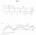
PREFERRED EMBODIMENTS OF THE INVENTIONThe advantageous effects of the present invention will be described below referring to FIGS. 1 and 2. FIG. 1(a) is a front view showing a heating resistance 1 according to an embodiment of the present invention, and FIG. 1(b) is a plan view showing a heating resistance 1. Further, FIG. 2(a) is a front view showing a heating resistance 1A according to another embodiment, and FIG. 2(b) is a plan view showing a heating resistance 1A.
FIG. 1 shows a heating resistance 1 composed of a band 5 made of a conductive material. The band 5 is elongated horizontally in FIG. 1 to form a band- or tape- or cord-shaped body. Many folds 2 extending in a direction perpendicular to the longitudinal direction of the heating resistance 1 are formed in the resistance 1 at a predetermined interval. A pair of wall parts 3a and 3b are formed on the both sides of the fold 2. A pair of wall parts 3a and 3b constitute one repetition unit 3. Further, “λ” represents a length (pitch) of one repetition unit 3, “B” represents an amplitude of the repetition unit 3, and “W” represents a width of the band 5.
FIG. 2 shows a heating resistance 1A composed of a band 5A made of a conductive material. The band 5A is elongated horizontally in FIG. 2 to form a band- or tape- or cord-shaped body. Many folds 2 extending in a direction perpendicular to the longitudinal direction of the heating resistance 1A are formed in the resistance 1A at a predetermined interval. A pair of wall parts 3a and 3b, or 4a and 4b, are formed on the both sides of the fold 2. A pair of wall parts 3a and 3b constitute one repetition unit 3, and a pair of wall parts 4a and 4b constitute one repetition unit. The repetition units 3 and 4 are continuously formed in one integrated band 5A.
“λ1” represents a length (pitch) of the repetition unit 3, “B1” represents an amplitude of the repetition unit 3, and “W1” represent a width of the band in the repetition unit 3. Further, “λ2” represents a length (pitch) of the repetition unit 4, “B2” represents an amplitude of the repetition unit 4, and “W2” represents a width of the band in the repetition unit 4. According to the present example, the amplitudes “B1” and “B2” are the same and the pitches “λ1” and “λ2” are the same in the repetition units 3 and 4. The width “W2” is, however, made larger than “W1”. The heating value per a unit length in the repetition unit 4 is made smaller than that in the repetition unit 3 when power is supplied to the heating resistance 1A in the longitudinal direction.
As can be seen from the examples of FIGS. 1 and 2, according to the heating resistance of the present invention, the pitches “λ”, “λ1”, “λ2”, amplitudes “B”, “B1”, “B2”, and widths “W”, “W1” “W2” in the repetition units 3 and 4 can be changed relatively easily and can be designed and manufactured at a high precision. It is thus possible to appropriately adjust the heating value per a unit length in any part of the heating resistance. For example, in every parts of the heating resistance, the pitch “λ” of the repetition unit can be easily controlled, by changing the position of the fold 2 and the angles of inclination of the wall parts 3a, 3b, 4a and 4b. Further, the amplitude “B” in the repetition unit can be easily controlled by changing the position of the fold 2 and the angles of inclination of the wall parts 3a, 3b, 4a and 4b. Further, the width “W” of the band can be easily adjusted by adjusting the width of the band when the band is produced. When the pitch, amplitude and width of the heating resistance is changed in the band, the band is continuous at interface where the pitch, amplitude or width is changed to prevent the risk of abnormal heat generation and disconnection. Further, the troublesome connecting process described earlier is not necessary for the production.
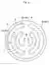
FIG. 3 is a plan view showing an example of planar pattern of the heating resistance 1 (or 1A) in a substrate 9 of a heater 8 (or 8A) according to one embodiment of the first aspect of the present invention. Although the substrate 9 substantially has a shape of a disk according to the present example, the shape of the substrate 9 is not particularly limited. Further, although the heating resistance 1 (1A) can be provided on the upper and lower surface of the substrate 9, the heating resistance 1 (1A) may preferably be embedded in the substrate 9. When the heating resistance 1 (1A) is embedded in the substrate 9, FIG. 3 schematically shows the planar pattern of the embedded heating resistance as a perspective projection.
For example, a pair of terminals 10 are embedded in a central part of the substrate 9 and electrically and mechanically connected with outer power supply cables not shown, respectively. The heating resistances 1 or 1A having the shape described above is connected to a pair of terminals 10. The heating resistance is positioned according to a predetermined spiral pattern so that the heating resistance surrounds the terminals 10.
For example, as schematically shown in FIG. 4(a), the pitch “λ”, amplitude “B” and width “W” can be made constant over the whole length of the heating resistance 1. In this case, the heating value per a unit length of the heating resistance can be made substantially constant over the whole length. If desired temperature distribution on the surface of the substrate 9 can be attained by this kind of design, it is not needed to consider another design type.
Depending on the design of the heater, however, it is required that the heating value is made larger in a part of the heating resistance than the other part of the resistance. In the example of FIG. 3, it is provided that a through hole is formed near the outer periphery of the substrate 9. In this case, it is difficult to embed the heating resistance 1 (heat source) in the proximity of the through hole 11 and calorific energy is escaped from the inner wall surface of the through hole 11. The temperature tends to be locally lowered in a region near the through hole 11 in the substrate 9. In this case, as shown in FIG. 4(b), the repetition units 3 having a smaller width are embedded in a specific region “D” near the through hole 11, and the repetition units 4 having a larger width are embedded in the other region. As a result, the heating value per a unit length is made relatively larger in the specific region “D” to supply an excessive calorific energy to the surface of the substrate 9 sufficient for compensating the absence of the heating resistance near the through hole 11 and the escape of heat from the inner wall surface of the through hole 11.
A second aspect of the present invention provides a heating resistance comprising a wound body of a band composed of a conductive material. The second aspect of the present invention further provides a heater comprising a substrate made of an insulating material and the above heating resistance fixed to the substrate.
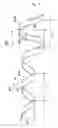
The advantageous effects will be described referring to FIGS. 5 to 7. FIG. 5 is a perspective view showing a heating resistance 12 according to an embodiment of the present invention, and FIGS. 6 and 7 are plan views showing heating resistances 12 and 12A, respectively.
The heating resistance 12 of FIGS. 5 and 6 is composed of a band 20 made of a conductive material. The band 20 is wound to a shape of a spiral or coil spring to form a heating resistance 12. In FIG. 6, “λ” represents a length (pitch) of one repetition unit 13 of the spiral, “E” represents the winding diameter (coil diameter) of the spiral, and “W” represents the width of the band 20.
In FIG. 7, bands 20A and 20 B having widths “W1” and “W2” different from each other are shaped to provide an integral and elongate body. “λ1” represents a length “pitch” of one repetition unit 13 of the spiral, “E1” represents a winding diameter of the spiral, and “W1” represents the width of the band 13. Further, “λ2” represents a length (pitch) of one repetition unit 14, “E2” represents the winding diameter of the spiral, and “W2” represents the width of the band 14.
According to the present example, the pitches λ1 and λ2 of the spiral are the same and the widths “W1” and “W2” of the bands 20A and 20B are the same in the repetition units 13 and 14. The winding diameter “E2” of the repetition unit 14 is, however, made larger than the winding diameter “E1” of the repetition unit 13. The heating value per a unit length of the heating resistance in the repetition unit 14 is made larger than that in the repetition unit 13 when power is supplied to the heating resistance 12A in the longitudinal direction.
Alternatively, the winding diameters and pitches can be made the same in the repetition units 13 and 14. In this case, the width “W1” (repetition unit 13) of the band 20A is made larger than the width “W2” (repetition unit 14) of the band 20B. The heating value per a unit length of the heating resistance in the repetition unit 14 is thus made larger than that in the repetition unit 13.
Alternatively, the widths and winding diameters can be made the same in the repetition units 13 and 14. In this case, the pitch “λ1” (repetition unit 13) of the band 20A is made larger than the pitch “λ2” (repetition unit 14) of the band 20B. The heating value per a unit length of the heating resistance in the repetition unit 14 is thus made larger than that in the repetition unit 13.
As can be seen from the examples shown in FIGS. 5 to 7, according to the heating resistance of the present invention, the pitches “λ”, “λ1” and “λ2” and winding diameters “E1” and “E2” of spiral and the widths “W”, “W1” and “W2” of the band in the repetition units 13 and 14 can be changed relatively easily and designed and manufactured at a high precision. It is thus possible to appropriately adjust the heating value per a unit length in any part of the heating resistance. When the pitch, winding diameter and width of the heating resistance is changed in the band, the band is continuous at interface where the pitch, winding diameter or width is changed to prevent the risk of abnormal heat generation and disconnection. Further, the troublesome connecting process described earlier is not necessary for the production.
FIG. 8 is a plan view showing an example of planar pattern of the heating resistance 12 (or 12A) in a substrate 9 of a heater 18 (or 18A) according to one embodiment of the second aspect of the present invention. Although the heating resistance 12 (12A) may be provided on the upper and lower surfaces of the substrate 9, the heating resistance 12 (12A) may preferably be embedded in the substrate 9. When the heating resistance 12 (12A) is embedded in the substrate 9, FIG. 8 schematically shows the planar pattern of the embedded heating resistance as a perspective projection.
The planar patterns of the embedded heating resistances 12 and 12A are the same as that shown in FIG. 3, and its explanation is omitted. According to the present example, as shown in FIG. 6, the pitch “λ”, winding diameter “E” and width “W” can be made substantially constant over the whole length of the heating resistance. In this case, the heating value per a unit length of the heating resistance can be made substantially constant over the whole length of the heating resistance.
Depending on the design of the heater, however, it may be required that the heating value is made larger in a part of the heating resistance than the other part of the resistance. In the example of FIG. 8, it is provided that a through hole 11 is formed near the outer periphery of the substrate 9. In this case, the temperature tends to be locally lowered in a region near the through hole 11 in the substrate 9. In this case, as shown in FIG. 7, the repetition units 14 having a larger winding diameter “E2” is embedded in a specific region “D” near the through hole 11, and the repetition units 13 having a smaller winding diameter “E1” are embedded in the other region. As a result, the heating value per a unit length is made relatively larger in the specific region “D” to supply an excessive calorific energy to the surface of the substrate 9 sufficient for compensating the absence of the heating resistance near the through hole 11 and the escape of heat from the wall inner surface the through hole 11.
In the first and second aspects of the present invention, the kind of object to be heated is not limited. Further, the application of the heating resistance and heater according to the present invention is not particularly limited, and may preferably a system for producing semiconductors. Such system means a system usable in a wide variety of semiconductor processing in which metal contamination of a semiconductor is to be avoided. Such system includes a film forming, etching, cleaning and testing systems.
The material for the heating resistance may preferably be tantalum, tungsten, molybdenum, platinum, rhenium, hafnium or the alloys of these metals. In particular, when the ceramic substrate is made of aluminum nitride, the material of the heating resistance may preferably be pure molybdenum or an alloy containing molybdenum. The material of the heating resistance may be a conductive material such as carbon, TiN or TiC, in addition to the high melting point metals described above.
The substrate for the heater may be made of a ceramic material or the other insulating materials not particularly limited. The material for the substrate may be a known ceramic material including a nitride ceramics such as aluminum nitride, silicon nitride, boron nitride and sialon, and an alumina-silicon carbide composite material. Aluminum nitride or alumina is most preferred for providing excellent anti-corrosion property against a corrosive gas such as a halogen based corrosive gas.
The shape of the substrate is not particularly limited and may preferably be a disk. Pocket shaped parts, emboss-shaped parts, or grooves may be formed on the heating face.
According to the first and second aspects of the present invention, the thickness of the band is not particularly limited. The thickness may preferably be 0.05 mm or larger for preventing the disconnection of the heating resistance. Further, the thickness may preferably be 5 mm or smaller on the viewpoint of easily deforming the band to a shape of spiral or bellows.
Further, in the first and second aspects of the present invention, a through hole may be formed in the band. It is possible to control the heating value generated from any part of the heating resistance, by controlling the shape, dimension and number of the through hole. Further, when the wave shaped body or wound body composed of a band having a through holes formed therein is embedded in an insulating substrate, it is possible to improve the adhesion of the insulating material, particularly ceramics, constituting the substrate.
FIG. 9(a) is a front view showing a heating resistance 1 according to this embodiment, and FIG. 9(b) is a plan view showing the heating resistance 1. According to the present example, many through holes 15 are formed in the band 5 at predetermined intervals. Further, FIG. 10 is a perspective view showing a heating resistance 12 according to the present embodiment. Many through holes 15 are formed in the band 20 at predetermined intervals.
EXAMPLES Example 1The heater 8 described referring to FIGS. 3 and 4(a) was produced and the temperature distribution on the surface 9a was measured.
Specifically, the substrate 9 was made of aluminum nitride sintered body having a diameter Ø of 350 mm and a thickness of 20 mm. The heating resistance 1 shown in FIGS. 1(a) and 1(b) was embedded in the substrate 9. The band 1 was formed of molybdenum and had a thickness of 0.2 mm and width “W” of 10 mm. The pitch “λ” of the repetition unit 3 was 1 to 7 mm and the amplitude “B” of the repetition unit 3 was 3 mm.
The temperature of the ceramic heater was raised so that the average temperature on the surface 9a reached about 500° C. The temperature distribution on the surface 9a was observed with a thermoviewer. FIG. 11(a) shows the thus obtained contour lines of temperature. The minimum temperature point of 493° C. was near the through holes 11. The maximum temperature point of 503° C. was on the outer periphery on the opposite side to the through hole 11. The difference of the maximum and minimum temperatures was 10° C. to prove that the temperature uniformity on the surface can be considerably improved.
Example 2The heater 8A described referring to FIGS. 3 and 4(b) was produced and the temperature distribution on the surface 9a was measured.
The heating resistance 1A shown in FIGS. 2(a) and 2(b) was embedded in the substrate 9. The band 5A was formed of molybdenum and had a thickness of 0.2 mm. The width “W1” was 7 mm, pitch “λ1” was 1 to 7 mm and amplitude “B1” was 3 mm in the repetition unit 3. The width “W2” was 10 mm which was larger than W1, pitch “λ2” was 1 to 7 mm and amplitude “B2” was 3 mm in the repetition unit 4.
The temperature of the ceramic heater was raised so that the average temperature on the surface 9a reached about 500° C. The temperature distribution on the surface 9a was observed with a thermoviewer. FIG. 11(b) shows the thus obtained contour lines of temperature. The minimum temperature point of 494° C. was observed at the outer periphery. The maximum temperature point of 501° C. was near the center of the surface 9a. The difference of the maximum and minimum temperatures was 7° C. to prove that the temperature uniformity on the surface can be considerably improved.
Example 3The heater 18 described referring to FIGS. 6 and 8 was produced and the temperature distribution on the surface 9a was measured.
Specifically, the substrate 9 was made of aluminum nitride sintered body had a diameter Ø of 350 mm and a thickness of 20 mm. The heating resistance 12 shown in FIG. 6 was embedded in the substrate 9. The band 20 was formed of molybdenum and had a thickness of 0.2 mm and a width “W” of 10 mm. The pitch “λ” was 1 to 7 mm the winding diameter “E” was 4 mm in the repetition unit 13.
The temperature of the ceramic heater was raised so that the average temperature on the surface 9a reached about 500° C. The temperature distribution on the surface 9a was observed with a thermoviewer. The difference of the maximum and minimum temperatures was 8° C. to prove that the temperature uniformity on the surface can be considerably improved.
Example 4The heater 18A described referring to FIGS. 7 and 8 was produced and the temperature distribution on the surface 9a was measured.
The heating resistance 12A shown in FIG. 7 was embedded in the substrate 9. The bands 20A and 20B were formed of molybdenum and had a thickness of 0.1 mm. The thickness “W1” was 10 mm, the pitch “λ1” was 1 to 7 mm and winding diameter “E1” was 4 mm in the repetition unit 13. The thickness “W2” was reduced to 7 mm, the pitch “λ2” was 1 to 7 mm and winding diameter “E2” was 4 mm and the same as “E1” in the repetition unit 14.
The temperature of the ceramic heater was raised so that the average temperature on the surface 9a reached about 500° C. The temperature distribution on the surface 9a was observed with a thermoviewer. The difference of the maximum and minimum temperatures was 5° C. to prove that the temperature uniformity on the surface can be considerably improved.
As described above, the present invention provides a heating resistance so that the heating value per a unit length can be easily designed and changed, and the reliability can be improved and abnormal heat generating can be prevented at the interface where the heating value per a unit length is changed.
The present invention has been explained referring to the preferred embodiments. However, the present invention is not limited to the illustrated embodiments which are given by way of examples only, and may be carried out in various modes without departing from the scope of the invention.
Claims
1. A heating resistance comprising a shaped body of a band made of a conductive material, said shaped body comprises a shape of a wave.
2. The heating resistance of claim 1, comprising a plurality of portions wherein at least one of the amplitude of said shaped body, pitch of said shaped body and width of said band is different from each other.
3. The heating resistance of claim 1, wherein a through holes is formed in said band.
4. The heating resistance of claim 2, wherein a through holes is formed in said band.
5. A heater comprising a substrate made of an insulating material and a heating resistance of claim 1 fixed to said substrate.
6. A heater comprising a substrate made of an insulating material and a heating resistance of claim 2 fixed to said substrate.
7. A heater comprising a substrate made of an insulating material and a heating resistance of claim 4 fixed to said substrate.
8. The heater of claim 5, wherein said heating resistance is embedded in said substrate.
9. The heater of claim 6, wherein said heating resistance is embedded in said substrate.
10. The heater of claim 7, wherein said heating resistance is embedded in said substrate.
11. A heating resistance comprising a wound body of a band made of a conductive material.
12. The heating resistance of claim 11, comprising a plurality of portions wherein at least one of the a winding diameter of said wound body, pitch of said wound body and width of said band is different from each other.
13. The heating resistance of claim 11, wherein a through holes is formed in said band.
14. The heating resistance of claim 12, wherein a through holes is formed in said band.
15. A heater comprising a substrate made of an insulating material and a heating resistance of claim 11 fixed to said substrate.
16. A heater comprising a substrate made of an insulating material and a heating resistance of claim 12 fixed to said substrate.
17. A heater comprising a substrate made of an insulating material and a heating resistance of claim 14 fixed to said substrate.
18. The heater of claim 15, wherein said heating resistance is embedded in said substrate.
19. The heater of claim 16, wherein said heating resistance is embedded in said substrate.
20. The heater of claim 17, wherein said heating resistance is embedded in said substrate.
Images & Drawings included:


Sources:
- United States Patent and Trademark Office - verify current appl. status at the USPTO↗
Similar patent applications:
- » 20150125134
HEAT-RESISTANT ELECTRIC HEATER - » 10887163
Resistive heater comprising first and second resistive traces, a fuser subassembly including such a resistive heater and a universal heating apparatus including first and second resistive traces - » 20250003637
METHOD AND SYSTEM FOR IMPLEMENTING ADVANCED OPERATING MODES IN ELECTRIC RESISTANCE WATER HEATERS AND HEAT PUMP WATER HEATERS - » 20160221680
Uniform heat distribution in resistive heaters for anti-icing and de-icing - » 20060186110
Electric heater with resistive carbon heating elements - » 20230112157
Method and system for implementing advanced operating modes in electric resistance water heaters and heat pump water heaters - » 20100116182
RESISTANCE HEATER BASED AIR HEATING DEVICE - » 20230110627
Uniform Heat Distribution in Resistive Heaters For Anti-Icing and De-Icing - » 20130014695
Ring-shaped resistance heater for supplying heat to a growing single crystal - » 20180119991
Electrical water heater with a dual resistive heating element and a control method for energy management
Recent applications in this class:
- » 20250220777 2025-07-03
Method and Apparatus of Substrate Support Repair and Refurbishment - » 20250024561 2025-01-16
CERAMIC HEATER - » 20230284341 2023-09-07
CERAMIC HEATER - » 20230247727 2023-08-03
Ceramic heater - » 20230209661 2023-06-29
METROLOGY DEVICE, SYSTEM AND METHOD - » 20220394822 2022-12-08
CERAMIC STRUCTURE AND WAFER SYSTEM - » 20220377850 2022-11-24
CERAMIC HEATER AND METHOD OF MANUFACTURING THE CERAMIC HEATER - » 20220279626 2022-09-01
Heated substrate support - » 20220110190 2022-04-07
Ceramic heater - » 20220030669 2022-01-27
CERAMIC HEATER WITH SHAFT
Recent applications for this Assignee:
- » 20250293081 2025-09-18
WAFER PLACEMENT TABLE - » 20250290699 2025-09-18
HEAT EXCHANGER - » 20250290697 2025-09-18
HEAT CONDUCTIVE MEMBER AND HEAT EXCHANGER - » 20250285909 2025-09-11
MEMBER FOR SEMICONDUCTOR MANUFACTURING EQUIPMENT - » 20250285844 2025-09-11
SUSCEPTOR - » 20250281873 2025-09-11
SEPARATION MEMBRANE SYSTEM - » 20250281869 2025-09-11
REACTOR AND METHOD FOR PRODUCING SAME, GAS RECOVERY DEVICE, AND GAS RECOVERY SYSTEM - » 20250281866 2025-09-11
HONEYCOMB STRUCTURE - » 20250280725 2025-09-04
METHOD OF PRODUCING PHOTOELECTRIC CONVERSION ELEMENT AND PHOTOELECTRIC CONVERSION ELEMENT - » 20250276268 2025-09-04
REACTOR, GAS RECOVERY DEVICE, AND GAS RECOVERY SYSTEM