Light emitting diode and fabrication method thereof
US20060054904A1
2006-03-16
11/042,116
2005-01-26
✅ Patent granted
US 7,339,197 B2
2008-03-04
-
-
Carl Whitehead, Jr. | Jennifer M. Dolan
2025-07-21
Abstract:
A light emitting diode. The light emitting diode comprises a lead frame, a plurality of light emitting chips in the lead frame, and a molding unit in an optical path of the light emitting chips, wherein the molding unit comprises a periodic microstructure.
Inventors:
- Sheng Bang Huang 3 🇹🇼 Changhua, Taiwan
- Sun Bin Yin 6 🇹🇼 Hsinchu, Taiwan
- Chao-Ying Lin 1 🇹🇼 Taipei, Taiwan
- Pel-Fang Chiang 1 🇹🇼 Hsinchu, Taiwan
Assignee:
- INDUSTRIAL TECHNOLOGY RESEARCH INSTITUTE 7,890 🇹🇼 HSINCHU, Taiwan
Interested in similar patents?
Get notified when new applications in this technology area are published.
Classification:
H01L25/0753 » CPC main
Assemblies consisting of a plurality of individual semiconductor or other solid state devices ; Multistep manufacturing processes thereof all the devices being of a type provided for in the same subgroup of groups - , e.g. assemblies of rectifier diodes the devices not having separate containers the devices being of a type provided for in group the devices being arranged next to each other
H01L33/44 » CPC further
Semiconductor devices with at least one potential-jump barrier or surface barrier specially adapted for light emission; Processes or apparatus specially adapted for the manufacture or treatment thereof or of parts thereof; Details thereof characterised by the coatings, e.g. passivation layer or anti-reflective coating
H01L33/54 » CPC further
Semiconductor devices with at least one potential-jump barrier or surface barrier specially adapted for light emission; Processes or apparatus specially adapted for the manufacture or treatment thereof or of parts thereof; Details thereof characterised by the semiconductor body packages; Encapsulations having a particular shape
H01L2924/1815 » CPC further
Indexing scheme for arrangements or methods for connecting or disconnecting semiconductor or solid-state bodies as covered by; Details of package parts other than the semiconductor or other solid state devices to be connected; Encapsulation Shape
H01L2933/0091 » CPC further
Details relating to devices covered by the group but not provided for in its subgroups Scattering means in or on the semiconductor body or semiconductor body package
H01L2924/0002 » CPC further
Indexing scheme for arrangements or methods for connecting or disconnecting semiconductor or solid-state bodies as covered by; Technical content checked by a classifier Not covered by any one of groups , and
H01L2924/00 » CPC further
Indexing scheme for arrangements or methods for connecting or disconnecting semiconductor or solid-state bodies as covered by
H01L21/00 IPC
Processes or apparatus adapted for the manufacture or treatment of semiconductor or solid state devices or of parts thereof
H01L33/00 IPC
Semiconductor devices with at least one potential-jump barrier or surface barrier specially adapted for light emission; Processes or apparatus specially adapted for the manufacture or treatment thereof or of parts thereof; Details thereof
Description
BACKGROUNDThe invention relates to a light emitting diode (LED), and more particularly to a LED with molding unit and fabrication method thereof.
Multi-chip LEDs comprise a plurality of different color light emitting chips. The most common white multi-chip LED is a RGB LED. RGB LEDs comprise red (R), green (G) and blue (B) light emitting chips for obtaining white light.
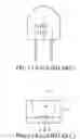
FIG. 1 shows a bullet type RGB LED structure. Red light emitting chip R, green light emitting chip G and blue light emitting B are disposed in the lead frame 10. The sidewalls of lead frame 10 comprise a highly reflective layer with a curvature for condensing the light emitted from the light emitting chips R, G and B. This type of LED further comprises lens type molding unit 12 to improve directionality thereof. A RGB LED has a good color mixing, the one would not see different color at different viewing angle. The light emitting chips R, G and B are positioned in different positions in the lead frame 10, however, the color-mixing effect of the bullet type LED is reduced. The lens type molding unit 12 reduces the color-mixing effect.
FIG. 2 shows a surface-mount device (SMD) RGB LED structure. The SMD RGB LED has no lens type molding unit, so its directionality is worse than the bullet type RGB LED. Furthermore, the surface of the lead frame 20 of the SMD RGB LED is uneven, thus the color-mixing effect and color uniformity are improved. At the same time, the uneven surface reflects and even scatters light, both of which decrease the SMD RGB LED directionality. In short, the SMD RGB LED improves color-mixing but reduces directionality.
Thus, the bullet type LED has good directionality, but bad color-mixing; the SMD type LED has bad directionality, but good color-mixing. Hence, there is a need for a LED with good directionality and good color-mixing characteristics.
SUMMARYAccordingly, embodiments of the invention provide a light emitting diode and fabrication method thereof.
A light emitting diode comprises a lead frame, a plurality of light emitting chips disposed in the lead frame, and a molding unit disposed in an optical path of the light emitting chips, wherein the molding unit comprises a periodic microstructure.
A light emitting diode fabrication method comprises providing a lead frame, providing a plurality of light emitting chips in the lead frame, patterning a surface of a molding unit to form a periodic microstructure, and setting the molding unit disposed in an optical path of the light emitting chips.
DESCRIPTION OF THE DRAWINGSFIG. 1 is a cross-section illustrating a conventional light emitting diode; conventional light emitting diode;
FIG. 3A is a cross-section illustrating a light emitting diode of the embodiments;
FIG. 3B is a cross-section illustrating another light emitting diode of the embodiments;
FIG. 4A˜4F are top-views illustrating the molding unit surface microstructure of the light emitting diode of the embodiments;
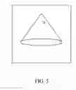
FIG. 5 is a schematic illustrating the half vertex angle of the light emitting diode;
FIG. 6A is a beam pattern illustrating the directionality of a conventional light emitting diode;
FIG. 6B is a color distribution illustrating the chromatic uniformity of a conventional light emitting diode;
FIG. 7A is a beam pattern illustrating the directionality of another conventional light emitting diode;
FIG. 7B is a color distribution illustrating the chromatic uniformity of another conventional light emitting diode;
FIG. 8A is a beam pattern illustrating the directionality of a light emitting diode of the first embodiment;
FIG. 8B is a color distribution illustrating the chromatic uniformity of a light emitting diode of the first embodiment;
FIG. 9A is a beam pattern illustrating the directionality at a different half vertex angle of a light emitting diode microstructure of the second embodiment;
FIG. 9B is a color distribution illustrating the chromatic uniformity at a different half vertex angle of a light emitting diode microstructure of the second embodiment;
FIG. 10 is a color distribution illustrating the chromatic uniformity of different light emitting chips in a given area of a light emitting diode of the third embodiment.
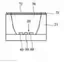
DETAILED DESCRIPTIONFIGS. 3A and 3B show multi-chip LEDs of the invention. The two LEDs comprise lead frame 10 (FIG. 3A) and lead frame 20 (FIG. 3B) respectively. The lead frame 10 comprises a smooth curved refrective surface to condense light. Two or more light emitting chips are disposed in the lead frame 10 and lead frame 20. In one embodiment, there are three light emitting chips 40, 50 and 60 in the lead frame 10 and lead frame 20 respectively. A main feature of the embodiment is the molding unit 70 with periodic microstructure 72.
Molding unit 70 is set in the optical path of the light emitting chips 40, 50 and 60 to condense light and mix color. The Molding unit 70 is transparent and the material thereof comprises epoxy or polymers. The polymers comprise polymethylmethacrylate (PMMA) or polycarbonate (PC). The molding unit 70 may be formed by a molding method. In this molding method, the melted epoxy or polymer mold is put in the mold, and the mold has a periodic microstructure. After solidification, the periodic microstructure of the mold is transferred to the epoxy or polymer molding unit 70 with periodic microstructure 72. The periodic microstructure of the mold may be formed by etching, cutting tools, laser or electron beam.
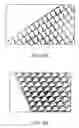
The periodic microstructure 72 of the molding unit 70 is a key feature of the invention. The microstructure comprises conical protrusions (FIG. 4A) or pyramidal protrusions. The pyramidal protrusions comprise symmetric pyramidal protrusions or asymmetric pyramidal protrusions. The symmetric pyramidal protrusions comprise a base which is symmetric triangular pyramidal, square pyramidal, symmetric pentangular pyramidal or symmetric hexangular pyramidal (FIG. 4B). The asymmetric pyramidal protrusions comprise a base which is asymmetric triangular pyramidal, asymmetric rectangular pyramidal (FIG. 4C), asymmetric pentangular pyramidal or asymmetric hexangular pyramidal.
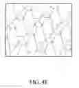
The periodic microstructure 72 of the molding unit 70 also comprises flat top conical protrusions or flat top pyramidal protrusions. The flat top pyramidal protrusions comprise flat top symmetric pyramidal protrusions or flat top asymmetric pyramidal protrusions. The flat top symmetric pyramidal protrusions comprise a base which is symmetric triangular pyramidal, square pyramidal (FIG. 4E), symmetric pentangular pyramidal or symmetric hexangular pyramidal. The flat top asymmetric pyramidal protrusions comprise a base which is asymmetric triangular pyramidal, asymmetric rectangular pyramidal, asymmetric pentangular pyramidal or asymmetric hexangular pyramidal.
Furthermore, the periodic microstructure 72 of the molding unit 70 comprises round top conical protrusions (FIG. 4F) or round top pyramidal protrusions. The round top pyramidal protrusions comprise round top symmetric pyramidal protrusions or round top asymmetric pyramidal protrusions. The round top symmetric pyramidal protrusions comprise a base which is symmetric triangular pyramidal, square pyramidal, symmetric pentangular pyramidal or symmetric hexangular pyramidal. The round top asymmetric pyramidal protrusions comprise a base which is asymmetric triangular pyramidal, asymmetric rectangular pyramidal, asymmetric pentangular pyramidal or asymmetric hexangular pyramidal.
In one embodiment, the bottom size of a single microstructure is preferably smaller than the size of the light emitting chip for improving directionality and color-mixing. The single microstructure bottom size is about 20 um˜1 nm, and preferably 20˜200 um. The height of and single microstructure is about 20 um˜1 mm, and preferably 20˜200 um. In one embodiment, the space between the single microstructures is preferably smaller than its bottom size to make sure that the emitted light passing through the molding unit. The space of the single microstructure is about 20 um˜1 nm, and preferably 20˜200 um.
The following embodiments are white RGB LED. The 30 present invention is not only used as a RGB LED or a white LED, but also as a white multi-chip LED and other multi-chip LEDs.
The directionality and color-mixing are obtained from the following measurement and calculation.
Chromatic Light Beam Pattern Intensity and Chromatic Uniformity Calculation
First, the three-color light in different “space angles luminous intensity” of the RGB LED of the invention is measured to obtain the RGB LED beam pattern. The directionality of RGB LED is determined by the FMWH of the beam pattern. The smaller the FMWH is, the better directionality of the RGB LED is.
The RGB LED 1960 CIE UCS color coordinates in respective space angle are obtained form the beam pattern and 20 mA spectra data of the red, green and blue light emitting chips. The chromatic aberrations of RGB LED in each space angles are calculated according to beam pattern, and the chromatic aberration definition as follows:
Δuv=[(u−u0)2−(v−v0)2]1/2
-
- wherein (u−u0) is the difference of the chromatic coordination at the RGB LED mechanical center, and (v−v0) is the difference of the chromatic coordination at each point of the RGB LED. A smaller chromatic aberration shows a higher chromatic uniformity of the device. In the invention, three space cross-sections 0°, 45° and 90° are analyzed to obtain the LED chromatic light space symmetry.
If the chromatic aberration is smaller than 0.008, it is difficult for the human eye to detect the color change. In practice, the color change must be unobvious (chromatic aberration <0.008) in ±30° space angle of LED.
First Comparative EmbodimentIn this embodiment, the RGB LED structure is the same as FIG. 1. The curvature radius of lens type molding unit 12 is 2.5 mm.
The chromatic light beam pattern distribution and chromatic uniformity of the RGB LED of this embodiment are shown in FIGS. 6A and 6B.
Second Comparative EmbodimentIn this embodiment, the RGB LED structure is the same as FIG. 2.
The chromatic light beam pattern distribution and chromatic uniformity of the RGB LED of this embodiment are shown in FIGS. 7A and 7B.
First EmbodimentIn this embodiment, the RGB LED structure is the same as FIG. 3B. Its microstructure 72 is conical protrusions with 46 half vertex angle (FIG. 5).
The chromatic light beam pattern distribution and chromatic uniformity of the RGB LED of this embodiment are shown in FIGS. 8A and 8B.
Second EmbodimentIn this embodiment, the RGB LED structures are the same as FIG. 3B. The microstructures 72 of the RGB LEDs are conical protrusions with 15°, 40°, 60° and 80° half vertex angle (FIG. 5).
The chromatic light beam pattern distribution and chromatic uniformity of the RGB LED of this embodiment are shown in FIGS. 9A and 9B.
Third EmbodimentIn this embodiment, the two RGB LED structures are the same as FIG. 3A. The microstructure 72 of the two RGB LEDs are conical protrusions with 46 half vertex angle (FIG. 5). The distance between light emitting chips of one RGB LED is 0.3 mm, another is 0.6 mm.
The chromatic uniformity of the RGB LED of this embodiment is show in FIG. 10.
Experiment Data and Invention Effect
1. Color-Mixing Improvement
The RGB LED of the comparative embodiment 1 is a bullet type LED, and has good directionality and bad color-mixing characteristics. After using the periodic microstructure molding unit (embodiment 1), good directionality and color-mixing characteristics can obtained at the same time:
Referring to FIGS. 6A and 8A, the FMWH of the comparative embodiment 1 and embodiment 1 RGB LEDs are about ±40°. In FIGS. 6B and 8B, the chromatic aberration of RGB LED of embodiment 1 is smaller than that of comparative embodiment 1. Furthermore, the three cross-section space aberrations of RGB LED of embodiment 1 are more uniform. That shows the RGB LED of the embodiment 1 not only has better color-mixing but also with better space symmetry. Thus, the molding unit can improve the bullet type LED color-mixing characteristics.
2. Directionality Improvement
The RGB LED of the comparative embodiment 2 is SMD LED, and has bad directionality and good color-mixing characteristics. After using the periodic microstructure molding unit (embodiment 2), good directionality and color-mixing characteristics can be obtained at the same time:
Referring to FIG. 9B, the RGB LEDs of comparative embodiment 2 and embodiment 2 all have good color-mixing characteristics. In FIG. 9A, the FMHW RGB LEDs of the embodiment 2 are narrower than that of the comparative embodiment 2. That shows the RGB LEDs of embodiment 2 have better directionality. Thus, the molding unit can improve the SMD LED directionality characteristics.
3. Half Vertex Angle Influence
Referring to FIGS. 9A and 9B, different vertex angles can influence the directionality and color-mixing characteristics, and the influence can be predicted by optical simulation calculation.
4. Light Emitting Chips distance Influence
Referring to FIG. 10, different light emitting chip arrangements can influence the directionality and color-mixing characteristics, and the influence can be predicted by optical simulation calculation.
The foregoing description has been presented for purposes of illustration and description. Obvious modifications or variations are possible in light of the above teaching. The embodiments were chosen and described to provide the best illustration of the principles of this invention and its practical application to thereby enable those skilled in the art to utilize the invention in various embodiments and with various modifications as are suited to the particular use contemplated. All such modifications and variations are within the scope of the invention as determined by the appended claims when interpreted in accordance with the breadth to which they are fairly, legally, and equitably entitled.
Claims
What is claimed is:1. A light emitting diode, comprising:
a lead frame;
a plurality of light emitting chips in the lead frame; and
a molding unit in an optical path of the light emitting chips, wherein the molding unit comprises a periodic microstructure.
2. The light emitting diode as claimed in claim 1 is a monochrome light emitting diode, a white light emitting diode or a full color light emitting diode.
3. The light emitting diode as claimed in claim 1, wherein the molding unit is transparent.
4. The light emitting diode as claimed in claim 1, wherein the periodic microstructure comprises conical protrusions or pyramidal protrusions.
5. The light emitting diode as claimed in claim 4, wherein the pyramidal protrusions comprise symmetric pyramidal protrusions or asymmetric pyramidal protrusions.
6. The light emitting diode as claimed in claim 5, wherein the symmetric pyramidal protrusions comprise a base which is symmetric triangular pyramidal, square pyramidal, symmetric pentangular pyramidal or symmetric hexangular pyramidal; the asymmetric pyramidal protrusions comprise a base which is asymmetric triangular pyramidal, asymmetric rectangular pyramidal, asymmetric pentangular pyramidal or asymmetric hexangular pyramidal.
7. The light emitting diode as claimed in claim 1, wherein the periodic microstructure comprises flat top conical protrusions or flat top pyramidal protrusions.
8. The light emitting diode as claimed in claim 7, wherein the flat top pyramidal protrusions comprise flat top symmetric pyramidal protrusions or flat top asymmetric pyramidal protrusions.
9. The light emitting diode as claimed in claim 8, wherein the flat top symmetric pyramidal protrusions comprise a base which is symmetric triangular pyramidal, square pyramidal, symmetric pentangular pyramidal or symmetric hexangular pyramidal; the flat top asymmetric pyramidal protrusions comprise a base which is asymmetric triangular pyramidal, asymmetric rectangular pyramidal, asymmetric pentangular pyramidal or asymmetric hexangular pyramidal.
10. The light emitting diode as claimed in claim 1, wherein the periodic microstructure comprises round top conical protrusions or round top pyramidal protrusions.
11. The light emitting diode as claimed in claim 10, wherein the round top pyramidal protrusions comprise round top symmetric pyramidal protrusions or round top asymmetric pyramidal protrusions.
12. The light emitting diode as claimed in claim 11, wherein the round top symmetric pyramidal protrusions comprise a base which is symmetric triangular pyramidal, square pyramidal, symmetric pentangular pyramidal or symmetric hexangular pyramidal; the round top asymmetric pyramidal protrusions comprise a base which is asymmetric triangular pyramidal, asymmetric rectangular pyramidal, asymmetric pentangular pyramidal or asymmetric hexangular pyramidal.
13. The light emitting diode as claimed in claim 1, wherein the microstructure has a size of about 20 um˜1 mm.
14. A light emitting diode fabrication method, comprising:
providing a lead frame;
providing a plurality of light emitting chips in the lead frame;
patterning a surface of a molding unit to form a periodic microstructure; and
setting the molding unit in an optical path of the light emitting chips.
15. The light emitting diode fabrication method as claimed in claim 14, wherein the light emitting diode is a monochrome light emitting diode, a white light emitting diode or a full color light emitting diode.
16. The light emitting diode fabrication method as claimed in claim 14, wherein the molding unit is transparent.
17. The light emitting diode fabrication method as claimed in claim 14, wherein the patterning step comprises modeling step.
18. The light emitting diode fabrication method as claimed in claim 17, wherein the molding step employs a mold having a microstructure thereon.
19. The light emitting diode fabrication method as claimed in claim 14, wherein periodic microstructure comprises conical protrusions or pyramidal protrusions.
20. The light emitting diode fabrication method as claimed in claim 19, wherein the pyramidal protrusions comprise symmetric pyramidal protrusions or asymmetric pyramidal protrusions.
21. The light emitting diode fabrication method as claimed in claim 20, wherein the symmetric pyramidal protrusions comprise a base which is symmetric triangular pyramidal, square pyramidal, symmetric pentangular pyramidal or symmetric hexangular pyramidal; the asymmetric pyramidal protrusions comprise a base which is asymmetric triangular pyramidal, asymmetric rectangular pyramidal, asymmetric pentangular pyramidal or asymmetric hexangular pyramidal.
22. The light emitting diode fabrication method as claimed in claim 14, wherein the periodic microstructure comprises flat top conical protrusions or flat top pyramidal protrusions.
23. The light emitting diode fabrication method as claimed in claim 22, wherein the flat top pyramidal protrusions comprise flat top symmetric pyramidal protrusions or flat top asymmetric pyramidal protrusions.
24. The light emitting diode fabrication method as claimed in claim 23, wherein the flat top symmetric pyramidal protrusions comprise a base which is symmetric triangular pyramidal, square pyramidal, symmetric pentangular pyramidal or symmetric hexangular pyramidal; the flat top asymmetric pyramidal protrusions comprise a base which is asymmetric triangular pyramidal, asymmetric rectangular pyramidal, asymmetric pentangular pyramidal or asymmetric hexangular pyramidal.
25. The light emitting diode fabrication method as claimed in claim 14, wherein the periodic microstructure comprises round top conical protrusions or round top pyramidal protrusions.
26. The light emitting diode fabrication method as claimed in claim 25, wherein the round top pyramidal protrusions comprise round top symmetric pyramidal protrusions or round top asymmetric pyramidal protrusions.
27. The light emitting diode fabrication method as claimed in claim 26, wherein the round top symmetric pyramidal protrusions comprise a base which is symmetric triangular pyramidal, square pyramidal, symmetric pentangular pyramidal or symmetric hexangular pyramidal; the round top asymmetric pyramidal protrusions comprise a base which is asymmetric triangular pyramidal, asymmetric rectangular pyramidal, asymmetric pentangular pyramidal or asymmetric hexangular pyramidal.
28. The light emitting diode fabrication method as claimed in claim 14, wherein the microstructure size is smaller than the light emitting chips size.
29. The light emitting diode fabrication method as claimed in claim 14, wherein the microstructure has a size of about 20 um˜1 mm.
Images & Drawings included:


Sources:
- United States Patent and Trademark Office - verify current appl. status at the USPTO↗
Similar patent applications:
- » 20060141644
Light emitting diode and fabricating method thereof - » 20060258029
Surface-emitting type light-emitting diode and fabrication method thereof - » 10636591
Surface-emitting type light-emitting diode and fabrication method thereof - » 20060113550
Gallium nitride-based light emitting diode and fabrication method thereof - » 20050017259
Chip light emitting diode and fabrication method thereof - » 20060163592
Light emitting diode and fabricating method thereof - » 20050221527
Light emitting diode and fabrication method thereof - » 20050133796
Nitride semiconductor light emitting diode and fabrication method thereof - » 11142082
Flip-chip light emitting diode and fabricating method thereof - » 20060292804
NITRIDE SEMICONDUCTOR LIGHT EMITTING DIODE AND FABRICATION METHOD THEREOF
Recent applications in this class:
- » 20250293216 2025-09-18
DISPLAY APPARATUS - » 20250293215 2025-09-18
LIGHT MIXING ARRANGEMENTS IN MULTIPLE-CHIP LIGHT-EMITTING DIODE PACKAGES - » 20250286023 2025-09-11
LED DISPLAY BOARD THAT CAN BE USED INDOORS AND OUTDOORS WITH IMPROVED THICKNESS, WEIGHT, AND BRIGHTNESS BY APPLYING AN ALUMINUM HEATING PLATE TO THE BACK OF THE PERFORATED PCB AND DOUBLING THE LED ELEMENTS - » 20250273635 2025-08-28
LIGHT EMITTING DISPLAY DEVICE - » 20250273634 2025-08-28
DISPLAY DEVICE - » 20250266405 2025-08-21
LIGHT BLOCKING LOUVER PANEL FOR AN LED LIGHT DISPLAY - » 20250266404 2025-08-21
DISPLAY DEVICE - » 20250259974 2025-08-14
ARRAY BASE PLATE AND BACKPLANE - » 20250259973 2025-08-14
ELECTRONIC PACKAGE DEVICE - » 20250253295 2025-08-07
DISPLAY DEVICE AND MANUFACTURING METHOD THEREOF
Recent applications for this Assignee:
- » 20250289330 2025-09-18
MOBILE VEHICLE CHARGING PROTECTION DEVICE FOR ELECTRICAL SAFETY IN LIVESTOCK HOUSES - » 20250287224 2025-09-11
COMMUNICATION DEVICE AND COMMUNICATION METHOD - » 20250286593 2025-09-11
COMMUNICATION DEVICE AND METHOD OF BEAM MANAGEMENT - » 20250284336 2025-09-11
SYSTEM AND METHOD FOR ADJUSTING IMAGE BASED ON PHYSIOLOGICAL INFORMATION AND POSTURE - » 20250281908 2025-09-11
ELECTROCATALYST COMPOSITION AND PREPARATION METHOD THEREOF - » 20250273403 2025-08-28
CAPACITOR AND ELECTRONIC DEVICE - » 20250271759 2025-08-28
POLYMER, POSITIVE PHOTORESIST COMPOSITION, AND METHOD FOR FORMING PATTERNED PHOTORESIST LAYER - » 20250265803 2025-08-21
MULTI-SENSOR COORDINATION METHOD, PROCESSING DEVICE, AND INFORMATION DISPLAY SYSTEM - » 20250263659 2025-08-21
METHOD AND KIT FOR PREPARING AN IMMUNE CELL DIFFERENTIATED FROM A STEM CELL - » 20250252547 2025-08-07
CORROSION POSITIONING SYSTEM, CORROSION INSPECTION VEHICLE AND CORROSION POSITIONING METHOD USING THE SAME