Fabricating method of wafer protection layers
US20060057778A1
2006-03-16
11/162,606
2005-09-16
✅ Patent granted
US 7,510,909 B2
2009-03-31
-
-
Thanhha Pham
2026-11-10
Abstract:
A fabricating method of wafer protection layers and a wafer structure are provided. The fabricating method includes providing a wafer first. The wafer includes pluralities of chips and has an active surface, a corresponding reverse surface and a plurality of pre-cut trenches on the active surface. On the active surface, pluralities of bumps are disposed. Next, a first curing-type protection layer and a pellicle are disposed over the active surface. Afterwards, the first curing-type protection layer is asked to contact the active surface. Besides, a second curing-type protection layer is disposed on the reverse surface. Afterward, the first and the second curing-type protection layer are cured. Finally, the wafer is cut through the pre-cut trenches to separate the chips from the wafer.
Assignee:
- ADVANCED SEMICONDUCTOR ENGINEERING, INC. 1,972 🇹🇼 Kaohsiung, Taiwan
Interested in similar patents?
Get notified when new applications in this technology area are published.
Classification:
H01L21/78 » CPC further
Processes or apparatus adapted for the manufacture or treatment of semiconductor or solid state devices or of parts thereof; Manufacture or treatment of devices consisting of a plurality of solid state components formed in or on a common substrate or of parts thereof; Manufacture of integrated circuit devices or of parts thereof; Manufacture or treatment of devices consisting of a plurality of solid state components or integrated circuits formed in, or on, a common substrate with subsequent division of the substrate into plural individual devices
H01L21/56 » CPC main
Processes or apparatus adapted for the manufacture or treatment of semiconductor or solid state devices or of parts thereof; Manufacture or treatment of semiconductor devices or of parts thereof the devices having at least one potential-jump barrier or surface barrier, e.g. PN junction, depletion layer or carrier concentration layer; Assembly of semiconductor devices using processes or apparatus not provided for in a single one of the subgroups - , e.g. sealing of a cap to a base of a container Encapsulations, e.g. encapsulation layers, coatings
H01L21/6835 » CPC further
Processes or apparatus adapted for the manufacture or treatment of semiconductor or solid state devices or of parts thereof; Apparatus specially adapted for handling semiconductor or electric solid state devices during manufacture or treatment thereof; Apparatus specially adapted for handling wafers during manufacture or treatment of semiconductor or electric solid state devices or components ; Apparatus not specifically provided for elsewhere for supporting or gripping using temporarily an auxiliary support
H01L24/27 » CPC further
Arrangements for connecting or disconnecting semiconductor or solid-state bodies; Methods or apparatus related thereto; Means for bonding being attached to, or being formed on, the surface to be connected, e.g. chip-to-package, die-attach, "first-level" interconnects; Manufacturing methods related thereto; Layer connectors, e.g. plate connectors, solder or adhesive layers; Manufacturing methods related thereto Manufacturing methods
H01L21/563 » CPC further
Processes or apparatus adapted for the manufacture or treatment of semiconductor or solid state devices or of parts thereof; Manufacture or treatment of semiconductor devices or of parts thereof the devices having at least one potential-jump barrier or surface barrier, e.g. PN junction, depletion layer or carrier concentration layer; Assembly of semiconductor devices using processes or apparatus not provided for in a single one of the subgroups - , e.g. sealing of a cap to a base of a container; Encapsulations, e.g. encapsulation layers, coatings Encapsulation of active face of flip-chip device, e.g. underfilling or underencapsulation of flip-chip, encapsulation preform on chip or mounting substrate
H01L23/544 » CPC further
Details of semiconductor or other solid state devices Marks applied to semiconductor devices , e.g. registration marks,
H01L2221/6834 » CPC further
Processes or apparatus adapted for the manufacture or treatment of semiconductor or solid state devices or of parts thereof covered by; Apparatus for handling semiconductor or electric solid state devices during manufacture or treatment thereof; Apparatus for handling wafers during manufacture or treatment of semiconductor or electric solid state devices or components; Apparatus not specifically provided for elsewhere for supporting or gripping using temporarily an auxiliary support used to protect an active side of a device or wafer
H01L2223/5448 » CPC further
Details relating to semiconductor or other solid state devices covered by the group; Marks applied to semiconductor devices or parts for use after dicing Located on chip prior to dicing and remaining on chip after dicing
H01L2224/05001 » CPC further
Indexing scheme for arrangements for connecting or disconnecting semiconductor or solid-state bodies and methods related thereto as covered by; Means for bonding being attached to, or being formed on, the surface to be connected, e.g. chip-to-package, die-attach, "first-level" interconnects; Manufacturing methods related thereto; Bonding areas; Manufacturing methods related thereto; Structure, shape, material or disposition of the bonding areas prior to the connecting process of an individual bonding area Internal layers
H01L2224/16 » CPC further
Indexing scheme for arrangements for connecting or disconnecting semiconductor or solid-state bodies and methods related thereto as covered by; Means for bonding being attached to, or being formed on, the surface to be connected, e.g. chip-to-package, die-attach, "first-level" interconnects; Manufacturing methods related thereto; Bump connectors; Manufacturing methods related thereto; Structure, shape, material or disposition of the bump connectors after the connecting process of an individual bump connector
H01L2224/274 » CPC further
Indexing scheme for arrangements for connecting or disconnecting semiconductor or solid-state bodies and methods related thereto as covered by; Means for bonding being attached to, or being formed on, the surface to be connected, e.g. chip-to-package, die-attach, "first-level" interconnects; Manufacturing methods related thereto; Layer connectors, e.g. plate connectors, solder or adhesive layers; Manufacturing methods related thereto; Manufacturing methods by blanket deposition of the material of the layer connector
H01L2224/73104 » CPC further
Indexing scheme for arrangements for connecting or disconnecting semiconductor or solid-state bodies and methods related thereto as covered by; Means for bonding being of different types provided for in two or more of groups; Location prior to the connecting process on the same surface; Bump and layer connectors the bump connector being embedded into the layer connector
H01L2924/3511 » CPC further
Indexing scheme for arrangements or methods for connecting or disconnecting semiconductor or solid-state bodies as covered by; Technical effects; Mechanical effects; Thermal stress Warping
H01L2924/181 » CPC further
Indexing scheme for arrangements or methods for connecting or disconnecting semiconductor or solid-state bodies as covered by; Details of package parts other than the semiconductor or other solid state devices to be connected Encapsulation
H01L2924/14 » CPC further
Indexing scheme for arrangements or methods for connecting or disconnecting semiconductor or solid-state bodies as covered by; Details of semiconductor or other solid state devices to be connected; Device type Integrated circuits
H01L2924/00 » CPC further
Indexing scheme for arrangements or methods for connecting or disconnecting semiconductor or solid-state bodies as covered by
H01L2924/00014 » CPC further
Indexing scheme for arrangements or methods for connecting or disconnecting semiconductor or solid-state bodies as covered by; Technical content checked by a classifier the subject-matter covered by the group, the symbol of which is combined with the symbol of this group, being disclosed without further technical details
H01L2224/05599 » CPC further
Indexing scheme for arrangements for connecting or disconnecting semiconductor or solid-state bodies and methods related thereto as covered by; Means for bonding being attached to, or being formed on, the surface to be connected, e.g. chip-to-package, die-attach, "first-level" interconnects; Manufacturing methods related thereto; Bonding areas; Manufacturing methods related thereto; Structure, shape, material or disposition of the bonding areas prior to the connecting process of an individual bonding area; External layer Material
H01L21/44 IPC
Processes or apparatus adapted for the manufacture or treatment of semiconductor or solid state devices or of parts thereof; Manufacture or treatment of semiconductor devices or of parts thereof the devices having at least one potential-jump barrier or surface barrier, e.g. PN junction, depletion layer or carrier concentration layer the devices having semiconductor bodies not provided for in groups, , , and with or without impurities, e.g. doping materials Manufacture of electrodes on semiconductor bodies using processes or apparatus not provided for in groups -
H01L21/48 IPC
Processes or apparatus adapted for the manufacture or treatment of semiconductor or solid state devices or of parts thereof; Manufacture or treatment of semiconductor devices or of parts thereof the devices having at least one potential-jump barrier or surface barrier, e.g. PN junction, depletion layer or carrier concentration layer Manufacture or treatment of parts, e.g. containers, prior to assembly of the devices, using processes not provided for in a single one of the subgroups -
H01L21/50 IPC
Processes or apparatus adapted for the manufacture or treatment of semiconductor or solid state devices or of parts thereof; Manufacture or treatment of semiconductor devices or of parts thereof the devices having at least one potential-jump barrier or surface barrier, e.g. PN junction, depletion layer or carrier concentration layer Assembly of semiconductor devices using processes or apparatus not provided for in a single one of the subgroups - , e.g. sealing of a cap to a base of a container
Description
CROSS-REFERENCE TO RELATED APPLICATIONThis application claims the priority benefit of Taiwan application serial no. 93127970, filed on Sep. 16, 2005. All disclosure of the Taiwan application is incorporated herein by reference.
BACKGROUND OF THE INVENTION1. Field of Invention
The present invention relates to a fabricating method of wafer protection layers, and particularly to a fabricating method of wafer protection layers capable of enhancing chip production yield.
2. Description of the Related Art
The modern world is undergoing a fundamental society transformation with exploding information, wherein electronic products are everywhere and penetrating into our daily life. No matter what daily fields we are talking about, in all fields, such as food, apparel, housing, transportation, education and entertainment, we can find the immense applications of the products with IC (integrated circuit) components. Along with nonstop advance of electronic technology, the new generation products with more complex and more impersonated functions are kicked off. In terms of electronic product outlooks, it follows a stream of light-slim-short-compact. The modern semiconductor processes of chips are accordingly geared-up towards the main stream.
Normally, after completing a plurality of chips on a wafer, it needs to cut off the wafer for separating the chips, followed by packaging. During dicing a wafer and packaging chips however, the wafer and chips are likely to be polluted by the environmental moisture, dust and other impurities, even worse, the wafer surface is scratched. All these, such as oxidation caused by moisture, short-circuits contributed by dusts or open-circuits resulted by surface scratching would produce various defects with the delicate chips used in different kinds of circuits and lead the high-valued chips to be garbage. Besides, lots of debris generated during dicing a wafer is adhesive on the surface not only to pollute chips, but also to scratch the chip surface. The more chips discard, the more expensive is the production cost of chips. A possible detention delivering resulted by poor production outcome and re-scheduling the chip production even suffers the reputation of a manufacture. All of these negative results are certainly unwished-for by manufactures.
From the above described, how to overcome the defects in the chip process caused by dusting, polluting and scratching for enhancing the production yield of packaged chips is an extremely urgent project.
SUMMARY OF THE INVENTIONAn object of the present invention is to provide a fabricating method of wafer protection layers suitable for protecting chip surfaces during the packaging and further for enhancing the production yield of packaged chips.
The present invention provides a fabricating method of wafer protection layers. At first, a wafer is provided, which includes a plurality of chips and has an active surface, a corresponding reverse surface and a plurality of pre-cut trenches on the active surface. On the active surface a plurality of bumps are disposed. Next, a first curing-type protection layer and a pellicle are disposed over the active surface. Then, the first curing-type protection layer contacts the active surface. Further, a second curing-type protection layer is disposed on the reverse surface of the wafer. Afterward, the first curing-type protection layer and the second curing-type protection layer are cured. Finally, the wafer is cut through the pre-cut trenches to separate the chips from the wafer. Wherein, the sequence of steps for disposing the second curing-type protection layer and the first curing-type protection layer with the pellicle are allowed to be adjusted depending on the need.
In the embodiment, the steps for disposing the first curing-type protection layer and the pellicle over the active surface can be, for example, the first curing-type protection layer is firstly disposed over the active surface, followed by disposing the pellicle on the first curing-type protection layer. Alternatively, the steps of disposing the first curing-type protection layer and the pellicle over the active surface can be, for example, disposing the first curing-type protection layer on the pellicle firstly, followed by disposing the first curing-type protection layer and the pellicle together over the active surface, and the first curing-type protection layer herein faces the active surface.
In addition, after disposing the second curing-type protection layer but prior to curing both the first curing-type protection layer and the second curing-type protection layer, for example, a step of removing the pellicle is further included. Alternatively, after making the first curing-type protection layer contact the active surface but prior to disposing the second curing-type protection layer, for example, a step of removing the pellicle is further included.
The method for the first curing-type protection layer to contact the active surface is, for example, laminating the pellicle. The material of the first curing-type protection layer and the second curing-type protection layer is, for example, acrylic, nonconductive material. The material of the first curing-type protection layer is, for example, transparent material or opaque material. Moreover, the material of the first curing-type protection layer and the second curing-type protection layer can be macromolecule material.
In addition, the pellicle can be an ultraviolet-curing pellicle. After disposing the second curing-type protection layer but prior to curing both the first curing-type protection layer and the second curing-type protection layer, for example, a step of ultraviolet-curing and removing the ultraviolet-curing pellicle is further included. Alternatively, after making the first curing-type protection layer to contact the active surface but prior to disposing the second curing-type protection layer, for example, a step of ultraviolet-curing and removing the ultraviolet-curing pellicle is further included.
In a short, with the fabricating method of wafer protection layers, since on both the active surface and the reverse surface of the chip, for example, curing-type protection layers, i.e. curing-type macromolecule material layers are disposed, the chip production yield after packaging is enhanced.
BRIEF DESCRIPTION OF THE DRAWINGSThe accompanying drawings are included to provide a further understanding of the invention, and are incorporated in and constitute a part of this specification. The drawings illustrate embodiments of the invention and, together with the description, serve for explaining the principles of the invention.
FIG. 1 is a block diagram showing a flowchart of a fabricating method of wafer protection layers provided by an embodiment of the present invention.
FIGS. 2A˜2G are section views showing the flowchart of the fabricating method of wafer protection layers in FIG. 1.
FIG. 3 is a block diagram showing a flowchart of a fabricating method of wafer protection layers provided by another embodiment of the present invention.
FIG. 4A and FIG. 4B are section views showing the flowchart of the fabricating method of wafer protection layers in FIG. 3.
DESCRIPTION OF THE EMBODIMENTSFIG. 1 is a block diagram showing a flowchart of a fabricating method of wafer protection layers provided by an embodiment of the present invention and FIGS. 2A˜2G are section views showing the flowchart of the fabricating method of wafer protection layers in FIG. 1.
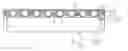
Referring to FIGS. 1 and 2A, a fabricating method of wafer protection layers provided by an embodiment of the present invention is begin with step S110 first, wherein a wafer 100 is provided. FIG. 2A is a schematic top view of the wafer 100. On the wafer 100 a plurality of chips 110 is formed. The wafer 100 is, for example, a silicon wafer commonly used in semiconductor industry. Continuing to FIGS. 1 and 2B, the wafer 100 has an active surface S1 and a corresponding reverse surface S2. In FIG. 2B only the partial wafer 100 with several chips is shown. On the active surface S1 a plurality of bumps 112 are disposed and used as electrically connecting paths between the circuit inside the chip 110 and other devices. Next at step S120, on the wafer 100, for example, a pre-cut trench 120 is formed. Alternatively, the pre-cut trench 120 was there on the wafer 100 already at step S110. Certainly, there can be another option, i.e., no pre-cut trench 120 on the wafer 100 at all. For some products, the pre-cut trench 120 is used for separating the chips 110 from each other.
Afterwards, referring to FIGS. 1 and 2C, at step S130, a first curing-type protection layer 130 is disposed over the active surface S1 of the wafer 100, wherein the first curing-type protection layer 130 is not closely adhered on the active surface S1 of the wafer 100 yet. The first curing-type protection layers, is, for example, a curing-type macromolecule material layers and preferred to be made of acrylic nonconductive material. Further, referring to FIGS. 1 and 2D, at step S140, a pellicle 140 is disposed on the first curing-type protection layer 130, followed by making the first curing-type protection layer 130 contact the active surface S1. Since the pellicle 140 has a considerable thickness and is not likely to adhere to the machines herein, a laminating machine is employed to exert an appropriate force onto the pellicle 140, so that the first curing-type protection layer 130 is down-pressed and laminated onto the active surface S1. Meanwhile it is preferred the first curing-type protection layer 130 is not be remained on the bumps 112. Besides, the pellicle 140 is, for example, an ultraviolet-curing pellicle; so that the pellicle 140 is easily to be removed once the pellicle 140 is exposed to ultraviolet light.
The material of the first curing-type protection layer 130 can be opaque material. At the point, if a pre-cut trench 120 was formed on the wafer 100 already, as the first curing-type protection layer 130 is down-pressed by the pellicle 140 onto the active surface S1, a part of first curing-type protection layer 130 would be sunken into the pre-cut trench 120 and a dent is formed, as shown in a localized enlargement drawing of FIG. 2E. The dent can be used for alignment during cutting the wafer in the subsequent process. Certainly, the material of the first curing-type protection layer 130 can be transparent material either, wherein if a pre-cut trench 120 was formed on the wafer 100 already, the transparency of the first curing-type protection layer 130 is in favor of viewing the pre-cut trench 120 and helpful for alignment during cutting the wafer in the subsequent process.
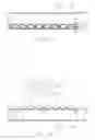
Furthermore, referring to FIG. 1 and 2E, at step S150, the pellicle 140 is removed. The method for removing the pellicle 140 is, for example, irradiating the pellicle 140 with ultraviolet light and then removing the pellicle 140. In succession, referring to FIG. 1 and 2F, at step S160, a second curing-type protection layer 150 is disposed on the reverse surface S2 of the wafer 100. The second curing-type protection layer 150 is, for example, a curing-type macromolecule material layer and preferred to be made of acrylic nonconductive material. The sequence of the processing steps can be changed depending on need. That is to say, the step S130 and S140 can be switched with the step S160. Thus, the step 160 for disposing the second curing-type protection layer 150 is prior to the step S130 and S140, where the first curing-type protection layer 130 and the pellicle 140 are disposed.
In the end, at step S170, the first curing-type protection layer 130 and the second curing-type protection layer 150 are cured. Besides, referring to FIGS. 1 and 2G, for example, the wafer 100 is cut off to separate chips 110 from the wafer 100 after step 170.
The second curing-type protection layer 150 is used for transferring the stress produced during cutting the wafer 100 onto itself, the second curing-type protection layer 150, so that the warpage of the chip back caused by stress concentration can be avoided and the chips are further protected from laser damaging during the subsequent laser marking process.
FIG. 3 is a block diagram showing a flowchart of a fabricating method of wafer protection layers provided by another embodiment of the present invention and FIG. 4A and FIG. 4B are section views showing the flowchart of the fabricating method of wafer protection layers in FIG. 3. Referring to FIGS. 3, 4A and 4B, the unique herein from the fabricating method of wafer protection layer shown in FIG. 1 is the sequence of step S250 and S260. Besides, the step S230 and S240 can be arranged after step S250 too.
In the fabricating method of wafer protection layers of FIG. 3, the second curing-type protection layer 150 is disposed on the reverse surface S2 of the wafer 100 first (step 250), followed by removing the pellicle 130 (step S260). The advantage thereof is that during disposing the second curing-type protection layer 150 the pellicle 140 is able to provide the bumps 112 with appropriate protection. The rest steps and the details in the fabricating method of wafer protection layers of FIG. 3 are the same as FIG. 1 and for simplicity, it is omitted to describe.
Remarkably, the fabricating method of wafer protection layers provided by the present invention doesn't limit the step sequence given by the above-described two embodiments in FIG. 1 and FIG. 3, where the first curing-type protection layer is disposed over the active surface first (step S130 and S230), then the pellicle is disposed on the first curing-type protection layer, followed by making the first curing-type protection layer contact the active surface (step S140 and S240). In more detail, in the fabricating method of wafer protection layers provided by the present invention, the first curing-type protection layer can be disposed on the pellicle first, then the first curing-type protection layer with the pellicle together are disposed on the active surface, followed by laminating the pellicle for the first curing-type protection layer to contact the active surface. No matter which step sequence is used, the final goal is the same that the first curing-type protection layer and the pellicle together are disposed on the active surface and then laminating is used for the first curing-type protection layer to contact the active surface.
Continuing to FIG. 2F, the wafer structure 200 provided by the present invention mainly includes a wafer 100, a first curing-type protection layer 130 and a second curing-type protection layer 150. The wafer 100 has an active surface S1 and a corresponding reverse surface S2. On the active surface S1 a plurality of bumps 112 are disposed. The first curing-type protection layer 130 is disposed on the active surface S1 and the bumps 112 on the active surface S1 are exposed without being covered by the first curing-type protection layer 130. The second curing-type protection layer 150 is disposed on the reverse surface S2 of the wafer 100. The first curing-type protection layer 130 and the second curing-type protection layer 150 can be macromolecule material layers.
Continuing to FIG. 2G, the chip structure 210, formed after the wafer structure 200 is cut off, but not limited to this way by the present invention, remains in the intelligent property scope protected by the present invention.
To sum up, in the chip structure, the wafer structure and the fabricating method of wafer protection layers provided by the present invention, since two curing-type protection layers, for example, two curing-type macromolecule material layers are disposed on the active surface and the reverse surface of the wafer/chips, respectively, the defects in the chip process caused by dusting, polluting or scratching can be avoided, which contributes to enhance the chip production yield after packaging. In addition, for a single chip, there are also two supplemental advantages. A supplemental advantage of the first curing-type protection layer is it takes over the function for fixing and protecting the bumps originally performed by underfill of the prior art. While a supplemental advantage of the second curing-type protection layer is it takes over the function for protecting the chip originally performed by molding compound of the prior art, so that a single chip after cutting the wafer is able to directly be joined onto a carrier of a circuit board. Besides, the pellicle, for example the ultraviolet-curing pellicle, is used for making the bumps breach the curing-type protection layer and securing the curing-type protection layer to be adhered on the active surface of a chip.
It will be apparent to those skilled in the art that various modifications and variations can be made to the structure of the present invention without departing from the scope or spirit of the invention. In view of the foregoing, it is intended that the specification and examples to be considered as exemplary only, with a true scope and spirit of the invention being indicated by the following claims and their equivalents.
Claims
What is claimed is:1. A fabricating method of wafer protection layers, comprising:
providing a wafer, the wafer comprises a plurality of chips and has an active surface, a corresponding reverse surface and a plurality of pre-cut trenches on the active surface, wherein a plurality of bumps are disposed on the active surface;
disposing a first curing-type protection layer and a pellicle over the active surface;
making the first curing-type protection layer contact the active surface;
disposing a second curing-type protection layer on the reverse surface;
curing the first curing-type protection layer and second curing-type protection layer; and
cutting the wafer through the pre-cut trenches to separate the chips from the wafer.
2. The fabricating method of wafer protection layers as recited in claim 1, wherein the steps for disposing the first curing-type protection layer and the pellicle over the active surface comprise:
disposing the first curing-type protection layer over the active surface; and
disposing the pellicle on the first curing-type protection layer.
3. The fabricating method of wafer protection layers as recited in claim 1, wherein the steps for disposing the first curing-type protection layer and the pellicle over the active surface comprise:
disposing the first curing-type protection layer on the pellicle; and
disposing the first curing-type protection layer and the pellicle together over the active surface and making the first curing-type protection layer face the active surface.
4. The fabricating method of wafer protection layers as recited in claim 1, wherein, after disposing the second curing-type protection layer but prior to curing the first curing-type protection layer and the second curing-type protection layer, a step for removing the pellicle is further comprised.
5. The fabricating method of wafer protection layers as recited in claim 1, wherein, after making the first curing-type protection layer contact the active surface but prior to disposing the second curing-type protection layer, a step for removing the pellicle is further comprised.
6. The fabricating method of wafer protection layers as recited in claim 1, wherein the method for making the first curing-type protection layer contact the active surface comprises laminating the pellicle.
7. The fabricating method of wafer protection layers as recited in claim 1, wherein the material of the first curing-type protection layer and the second curing-type protection layer comprises acrylic nonconductive material.
8. The fabricating method of wafer protection layers as recited in claim 1, wherein the material of the first curing-type protection layer comprises transparent material.
9. The fabricating method of wafer protection layers as recited in claim 1, wherein the material of the first curing-type protection layer comprises opaque material.
10. The fabricating method of wafer protection layers as recited in claim 1, wherein the material of the first curing-type protection layer and the second curing-type protection layer comprises macromolecule material.
11. The fabricating method of wafer protection layers as recited in claim 1, wherein the pellicle comprises an ultraviolet-curing pellicle.
12. The fabricating method of wafer protection layers as recited in claim 11, wherein, after disposing the second curing-type protection layer but prior to curing the first curing-type protection layer and the second curing-type protection layer, a step for ultraviolet-curing and removing the ultraviolet-curing pellicle is further comprised.
13. The fabricating method of wafer protection layers as recited in claim 11, wherein, after making the first curing-type protection layer contact the active surface but prior to disposing the second curing-type protection layer, a step for ultraviolet-curing and removing the ultraviolet-curing pellicle is further comprised.
Images & Drawings included:


Sources:
- United States Patent and Trademark Office - verify current appl. status at the USPTO↗
Similar patent applications:
Recent applications in this class:
- » 20250293050 2025-09-18
WAFER PROCESSING METHOD AND WAFER PROCESSING APPARATUS - » 20250273481 2025-08-28
METHOD OF MANUFACTURING SEMICONDUCTOR DEVICES AND CORRESPONDING DEVICE - » 20250210375 2025-06-26
SURFACE TREATMENT COMPOSITION AND METHOD FOR PRODUCING WAFER - » 20250191939 2025-06-12
SEMICONDUCTOR DEVICES AND METHODS OF MANUFACTURING - » 20250191938 2025-06-12
Overmolding Structures in Glass - » 20250149346 2025-05-08
METHOD OF FORMING ELECTROMAGNETIC-WAVE SHIELD, METHOD OF MANUFACTURING STRUCTURE, AND STRUCTURE - » 20250096008 2025-03-20
PACKAGED SEMICONDUCTOR DEVICES AND METHODS OF PACKAGING SEMICONDUCTOR DEVICES - » 20250062137 2025-02-20
POWER SEMICONDUCTOR MODULE ARRANGEMENT AND METHOD FOR PRODUCING THE SAME - » 20250062136 2025-02-20
Packages with Implantation - » 20250014912 2025-01-09
METHOD FOR PROTECTING ACTIVE LAYERS OF ELECTRONIC CHIPS
Recent applications for this Assignee:
- » 20250294670 2025-09-18
ELECTRONIC DEVICE - » 20250293221 2025-09-18
ELECTRONIC DEVICE - » 20250285950 2025-09-11
SEMICONDUCTOR DEVICE PACKAGE - » 20250282612 2025-09-11
PACKAGE STRUCTURE - » 20250273638 2025-08-28
SEMICONDUCTOR DEVICE PACKAGE INCLUDING STRESS BUFFERING LAYER - » 20250273531 2025-08-28
PACKAGE STRUCTURE - » 20250271555 2025-08-28
OPTOELECTRONIC STRUCTURE - » 20250266313 2025-08-21
SEMICONDUCTOR DEVICE PACKAGE AND METHOD OF MANUFACTURING THE SAME - » 20250260153 2025-08-14
ELECTRONIC DEVICE - » 20250259978 2025-08-14
SEMICONDUCTOR PACKAGE DEVICE AND METHOD OF MANUFACTURING THE SAME