Process for removing a residue from a metal structure on a semiconductor substrate
US20060108324A1
2006-05-25
10/995,025
2004-11-22
✅ Patent granted
US 7,413,993 B2
2008-08-19
-
-
Lan Vinh
2025-01-08
Abstract:
The invention is concerned with a process for removing residue comprising a polymeric resist and metal oxide from a metal structure on a semiconductor substrate, the process comprising the steps of: (a) heating up the substrate with the metal structure in the presence of molecular nitrogen gas (N2); (b) a stabilization step in the presence of pure molecular nitrogen gas (N2); (c) a passivation step employing a plasma containing at least one of the group of water, nitrogen and oxygen; and (d) a stripping step containing oxygen to remove the residue, comprising resist.
Inventors:
- Uwe KAHLER 5 🇩🇪 Dresden, Germany
- Chung-Hsin Lin 3 🇩🇪 Dresden, Germany
- Ronald Gottzein 1 🇩🇪 Dresden, Germany
- Jens Bachmann 6 🇩🇪 Dresden, Germany
- Dirk Efferenn 5 🇩🇪 Dresden, Germany
- Wen-Bin Lin 2 🇩🇪 Dresden, Germany
- Lee Donohue 1 🇩🇪 Dresden, Germany
Assignee:
- NANYA TECHNOLOGY CORPORATION 517 🇹🇼 Taoyuan, Taiwan
- Infineon Technologies AG 4,173 🇩🇪 Munich, Germany
Interested in similar patents?
Get notified when new applications in this technology area are published.
Classification:
G03F7/427 » CPC main
Photomechanical, e.g. photolithographic, production of textured or patterned surfaces, e.g. printing surfaces; Materials therefor, e.g. comprising photoresists; Apparatus specially adapted therefor; Processing photosensitive materials; Apparatus therefor; Stripping or agents therefor using plasma means only
C23G5/00 » CPC further
Cleaning or de-greasing metallic material by other methods; Apparatus for cleaning or de-greasing metallic material with organic solvents
H01J37/32192 » CPC further
Discharge tubes with provision for introducing objects or material to be exposed to the discharge, e.g. for the purpose of examination or processing thereof; Gas-filled discharge tubes; Arrangements for generation of plasma specially adapted for examination or treatment of objects, e.g. plasma sources Microwave generated discharge
H01L21/02071 » CPC further
Processes or apparatus adapted for the manufacture or treatment of semiconductor or solid state devices or of parts thereof; Manufacture or treatment of semiconductor devices or of parts thereof; Cleaning; Cleaning during device manufacture during, before or after processing of conductive layers, e.g. polysilicon or amorphous silicon layers the processing being a delineation, e.g. RIE, of conductive layers
H01J2237/3342 » CPC further
Discharge tubes exposing object to beam, e.g. for analysis treatment, etching, imaging; Processing objects by plasma generation characterised by the type of processing; Etching Resist stripping
C23G1/00 IPC
Cleaning or pickling metallic material with solutions or molten salts
B44C1/22 IPC
Processes, not specifically provided for elsewhere, for producing decorative surface effects Removing surface-material, e.g. by engraving, by etching
H01L21/302 IPC
Processes or apparatus adapted for the manufacture or treatment of semiconductor or solid state devices or of parts thereof; Manufacture or treatment of semiconductor devices or of parts thereof the devices having at least one potential-jump barrier or surface barrier, e.g. PN junction, depletion layer or carrier concentration layer the devices having semiconductor bodies comprising elements of Group IV of the Periodic System or AB compounds with or without impurities, e.g. doping materials; Treatment of semiconductor bodies using processes or apparatus not provided for in groups - to change their surface-physical characteristics or shape, e.g. etching, polishing, cutting
Description
TECHNICAL FIELDThis invention relates to a process for removing a residue from a metal structure on a semiconductor substrate.
BACKGROUNDIn semiconductor chips such as DRAM (dynamic random access memory) chips metal structures (e.g., aluminium lines) are used to electrically connect devices on those chips.
The metal structures for semiconductor chips are formed by first depositing the metal with, e.g., a chemical or physical vapor deposition process, on a substrate. Then a polymeric resist material is placed on the metal layer, which is then patterned through lithographic processes.
After the patterning, some of the resist material is removed so that the remaining resist material forms a mask for the following etching of the metal layer. Typical etching chemistries for plasma etching, e.g., for aluminium layers, employ halogen containing etching materials, like BCl3, BCl3/Cl2 or Br and F-containing gases. In general metal layers are etched by halogen containing plasmas.
After the etching of the metal layer, the remaining residue, containing resist with aluminium oxide, is removed by a dry stripping step usually followed by a wet clean process involving commercial or proprietary solutions. Further the residue can also contain silicon (incorporated from the SiO2 layer below the metal layer) and chlorine (which if of sufficient concentration can initiate corrosion of the amphoteric metal lines). Hence the semiconductor substrate can be further processed.
The processing outlined above is described, e.g., in the book by S. A. Campbell “The Science and Engineering of Microelectronic Fabrication”, Oxford University Press, 2001, which is incorporated herein by reference.
One problem of this known processing is that the residue, containing the polymeric resist with complex aluminium oxide, is difficult to remove in the stripping step without damaging the metal lines, especially aluminium lines. Also, at low dimensional technology nodes (e.g. 90 nm or lower) the use of DUV resist is preferred which can lead to increased sidewall residue thicknesses and reduced strip effectivity.
It is known, e.g., from U.S. Pat. No. 5,545,289 ('289 patent) to strip the polymeric resist and other residues with a plasma containing oxygen and an oxygen activating gas such as CF4 or N2. But as is mentioned in the prior art document, those steps are sometimes ineffective. A passivation step is used to reduce post-etch corrosion problems in the metal lines. The solution described in the '289 patent utilizes a multicycle process of the stripping and passivation steps to improve the removal of the polymeric resist. This makes the process more complex. The ’289 patent is incorporated herein by reference.
Furthermore, experience has shown that such known methods are ineffective when the residue has a high metal oxide concentration, e.g., a high aluminium oxide concentration.
SUMMARY OF THE INVENTIONThe process of embodiments of the present invention achieves the removal of the residue comprising polymeric resist and complex metal oxide through a special pre-treatment of the substrate with the metal structure and the polymeric remaining attached to it.
The pre-treatment comprises two process steps: a special heat up step a); and a special stabilization step b). According to the preferred embodiment of the invention, the heating up of the substrate with the metal structure and the stabilisation step take place in the presence of nitrogen gas following metal etch and without bringing the substrate to normal atmospheric conditions.
These steps are then followed by a passivation step c) employing a plasma containing at least one of the group of water, nitrogen and oxygen, and stripping step d) to prevent corrosion and to remove the residue, comprising resist.
It has been found that the in situ pre-treatment in the heating up step and the stabilization step under nitrogen gas allows for a complete and corrosion-free removal of the residue in the following wet strip step. This may be due to suppression of oxidation processes through the presence of a reducing gas and/or possibly through surface reaction/micro-diffusion processes. This allows modification of the residue such that conventional wet strip becomes totally effective.
The pre-treatment steps (heating up step a), stabilization step b)) can be conducted under pure nitrogen atmosphere or with a mixture containing nitrogen gas and oxygen gas.
A temperature range for all process steps is 20 to 400° C., preferably at a temperature of 280° C.
The heating up process step a) is conducted for a time longer than 2 seconds, preferably for 15 seconds. Whereas stabilization step b) is conducted for a duration between 1 and 20 seconds, preferably for 5 seconds.
The heating up step a) and the stabilization step b) are conducted with a volumetric flow rate greater than 10 sccm nitrogen gas (N2), preferably with a volumetric flow rate of 1000 sccm nitrogen gas (N2).
The total gas pressure in the heating up step a) and the stabilization step b) is 1 Torr, preferably in the range from 0.2 to 10 Torr.
Both the passivation step c) and the stripping step d) comprise a plasma etch process, especially a downstream TCP (ICP) process operating at 13,56 MHz. The stripping step d) can also comprise a plasma-etch process, involving CF4 as agent. Furthermore, the stripping process can also comprise the application of a microwave plasma generation process, the microwave radiation usually having a frequency in the Gigahertz (e.g., 2.45 GHz) range.
BRIEF DESCRIPTION OF THE DRAWINGSThese and other features of the present invention will be further described from the following drawings, description and appended claims, where:
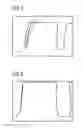
FIG. 1 is taken from a SEM image depicting a cross-section of an aluminium line with residue remaining after a stripping process according to the prior art; and
FIG. 2 is taken from a SEM image depicting a cross-section of an aluminium line after a stripping process according to an embodiment of the present invention.
DETAILED DESCRIPTION OF ILLUSTRATIVE EMBODIMENTSFIG. 1 shows a cross-section of an aluminium line 1 on an integrated circuit chip. In one example, the chip is a DRAM chip, although it is understood that other IC's can utilize concepts of the invention. The aluminium line 1 electrically connects different devices on the chip, not depicted here.
Around the aluminium line 1 some residue 2 is visible. It is especially noteworthy that the residue 2 extends above the top level of the aluminium line 1 forming peaks.
The depicted situation shows the metal line 1 and the residue 2 after a passivation and stripping step for a resist, the stripping process comprising first a plasma etch and then a wet etch step. As can be seen from FIG. 1, residue comprising polymeric resist could not be removed through the wet-etch step known from prior art. The complicating fact is that the residue 2 contains metal oxide, here primarily aluminium oxide, which makes it difficult to remove the residue 2 without damaging the aluminium line 1.
FIG. 2 in contrast shows the result achieved by using an embodiment of the present invention. The present invention introduces a pre-treatment of the substrate with the metal line, here an aluminium line, i.e., a heating up step and a stabilization step. In both steps it is important that the process steps are conducted in the presence of nitrogen gas, either pure nitrogen gas or a mixture of nitrogen and oxygen gases. The other process steps (passivation, stripping) were left unchanged.
The process conditions for the heating up step are:
| Pressure | 1 Torr | |
| Volumetric flow rate nitrogen gas | 1000 sccm (pure nitrogen) | |
| Duration | 15 seconds | |
| Position of substrate | Wafer pins down | |
The process conditions for the stabilization step are:
| Pressure | 1 Torr | |
| Volumetric flow rate nitrogen gas | 1000 sccm (pure nitrogen) | |
| Duration | 5 seconds | |
| Position of substrate | Wafer pins down | |
After this a passivation in a plasma chamber in the presence of water vapor is conducted with the following parameters:
| Pressure | 1 Torr | |
| Power | 1500 W | |
| Volumetric flow rate nitrogen gas | 500 sccm | |
| Volumetric flow rate water vapor | 2800 sccm | |
| Duration | 45 seconds | |
| Position of substrate | Wafer pins down | |
The plasma chamber as such is known in the prior art, e.g., from the above-cited documents.
The final removal of the resist is achieved in a stripping process comprising a plasma etch with the following parameters:
| Pressure | 1 Torr | |
| Power | 2400 W | |
| Volumetric flow rate oxygen gas | 4000 sccm | |
| Volumetric flow rate nitrogen | 280 sccm | |
| Duration | 90 seconds | |
| Position of substrate | Wafer pins down | |
| Wafer temperature for all process steps | typically 280° C. | |
This is followed by a wet-etch step also known from the prior art, which can use variety commercially or proprietary available solutions, e.g., EKC or DSP.
As can be seen, the result of the two pre-treatment steps, the heating up and the stabilization is much better removal of the residue.
Claims
What is claimed is:1. A process for removing residue comprising a polymeric resist and metal oxide from a metal structure on a semiconductor substrate, the process comprising the steps of:
(a) heating up the substrate with the metal structure in the presence of molecular nitrogen gas;
(b) performing a stabilization step in the presence of molecular nitrogen gas;
(c) performing a passivation step employing a plasma containing at least one of the group of water, nitrogen and oxygen; and
(d) performing a stripping step containing oxygen to remove the residue.
2. The process according to claim 1, wherein process step d) is followed by a vacuum-plasma modification of the residue and an exsitu solution clean step to remove any remaining residue.
3. The process according to claim 1, wherein the heating up step a) is conducted in the presence of pure nitrogen gas.
4. The process according to claim 1, wherein the heating up step a) is conducted in the presence of a mixture of nitrogen gas and oxygen gas.
5. The process according to claim 1, wherein the stabilization step b) is conducted in the presence of pure nitrogen gas.
6. The process according to claim 1, wherein the stabilization step b) is conducted in the presence of a mixture of nitrogen gas and oxygen gas.
7. The process according to claim 1, wherein at least one of the process steps is conducted in a temperature range of 20 to 400° C.
8. The process according to claim 1, wherein the heating up step a) is conducted for a time longer than 2 seconds.
9. The process according to claim 8, wherein the heating up step a) is conducted for a time longer than 15 seconds.
10. The process according to claim 1, wherein the stabilisation step b) is conducted for a duration between 1 and 20 seconds.
11. The process according to claim 1, wherein the heating up step a) is conducted with a volumetric flow rate of greater than 10 sccm nitrogen gas.
12. The process according to claim 11, wherein the heating up step a) is conducted with a volumetric flow rate of greater than 1000 sccm nitrogen gas
13. The process according to claim 1, wherein the stabilisation step b) is conducted with a volumetric flow rate of greater than 10 sccm nitrogen gas.
14. The process according to claim 13, wherein the stabilisation step b) is conducted with a volumetric flow rate of greater than 1000 sccm nitrogen gas.
15. The process according to claim 1, wherein the total gas pressure in the heat up step a) and the stabilization step is in the range from 0.2 to 10 Torr.
16. The process according to claim 1, wherein the stripping process comprises a plasma etch process.
17. The process according to claim 13, wherein the plasma etching is a TCP (ICP) process operating at 13,56 MHz.
18. The process according to claim 1, wherein the stripping step comprises a plasma process.
19. The process according to claim 18, wherein the stripping step uses CF4 as agent
20. The process according to claim 1, wherein the stripping process comprises the application of a microwave process, the microwave radiation having a frequency in the Gigahertz range.
21. The process according to claim 1, wherein the process is used in the production of a semiconductor device using lithography technology with exposure wavelengths selected from the group of 193 and 248 nm and provides metal structures for a dimensional technology node of 170 nm or less.
22. The process according to claim 21, wherein the dimensional technology node is less than 110 nm.
23. The process according to claim 1, wherein the metal structure comprises aluminium or aluminium-copper alloy.
24. The process according to claim 1, wherein the residue comprises a compound based on aluminium oxide.
25. The process according to claim 24, wherein the reside includes at least one of Si, C, Cl, F and Br.
26. The process according to claim 1, and further comprising performing a cleaning step using a wet solution after the stripping step.
Images & Drawings included:

Sources:
- United States Patent and Trademark Office - verify current appl. status at the USPTO↗
Recent applications in this class:
- » 20250237959 2025-07-24
PLASMA MULTI-WAFER ASHING SYSTEM - » 20250093781 2025-03-20
REWORK OF METAL-CONTAINING PHOTORESIST - » 20240288776 2024-08-29
METHOD FOR REMOVING RESIST LAYER, METHOD OF FORMING A PATTERN AND METHOD OF MANUFACTURING A PACKAGE - » 20230408926 2023-12-21
PLASMA-ACTIVATED LIQUIDS - » 20220229369 2022-07-21
Method for removing resist layer, method of forming a pattern and method of manufacturing a package - » 20200272057 2020-08-27
Resist removing method and resist removing apparatus - » 20200218158 2020-07-09
Strip process for high aspect ratio structure - » 20200218157 2020-07-09
PLASMA PROCESSING METHOD FOR PROCESSING SUBSTRATE - » 20200133133 2020-04-30
Plasma treatment method to improve photo resist roughness and remove photo resist scum - » 20200133132 2020-04-30
Method for removing photoresistor layer, method of forming a pattern and method of manufacturing a package
Recent applications for this Assignee:
- » 20190222018 2019-07-18
Temperature sensing and fault detection for paralleled double-side cooled power modules - » 20190120879 2019-04-25
Readout circuit for resistive and capacitive sensors - » 20190109113 2019-04-11
Semiconductor apparatus and method for preparing the same - » 20190081018 2019-03-14
Method for preparing a semiconductor package - » 20180374818 2018-12-27
Method for preparing a semiconductor apparatus - » 20180233486 2018-08-16
Die device, semiconductor device and method for making the same - » 20180226332 2018-08-09
Package structure and manufacturing method thereof - » 20180197284 2018-07-12
Method of recognizing wafer - » 20180196769 2018-07-12
Comparative forwarding circuit providing first datum and second datum to one of first circuit and second circuit according to target address - » 20180190607 2018-07-05
Semiconductor package and method for preparing the same