Integrated circuit chip having pass-through vias therein that extend between multiple integrated circuits on the chip
US20060118972A1
2006-06-08
11/339,973
2006-01-26
✅ Patent granted
US 7,595,559 B2
2009-09-29
-
-
Leonardo Andújar
2027-05-07
Abstract:
Packaged integrated circuit devices include a package substrate and a multi-chip stack of integrated circuit devices on the package substrate. The multi-chip stack includes at least one chip-select rerouting conductor. This rerouting conductor extends from the package substrate to a chip pad on an upper one of the chips in the multi-chip stack. The chip-select rerouting conductor extends through a first via hole in a lower one of the chips in the multi-chip stack.
Inventors:
- Young Hee SONG 17 🇰🇷 Gyeonggi-do, South Korea
- Dong-hyeon Jang 8 🇰🇷 Gyeonggi-do, South Korea
- In-young LEE 19 🇰🇷 Gyeonggi-do, South Korea
- Seung-Duk Baek 16 🇰🇷 Gyeonggi-do, South Korea
- Hyun-Soo CHUNG 15 🇰🇷 Gyeonggi-do, South Korea
- Sung-Min SIM 6 🇰🇷 Gyeonggi-do, South Korea
- Myeong-Soon PARK 3 🇰🇷 Gyeonggi-do, South Korea
Assignee:
- Samsung Electronics Co., Ltd 16,186 🇰🇷 , South Korea
Interested in similar patents?
Get notified when new applications in this technology area are published.
Classification:
H01L23/481 » CPC main
Details of semiconductor or other solid state devices; Arrangements for conducting electric current to or from the solid state body in operation, e.g. leads, terminal arrangements ; Selection of materials therefor Internal lead connections, e.g. via connections, feedthrough structures
H01L21/78 » CPC further
Processes or apparatus adapted for the manufacture or treatment of semiconductor or solid state devices or of parts thereof; Manufacture or treatment of devices consisting of a plurality of solid state components formed in or on a common substrate or of parts thereof; Manufacture of integrated circuit devices or of parts thereof; Manufacture or treatment of devices consisting of a plurality of solid state components or integrated circuits formed in, or on, a common substrate with subsequent division of the substrate into plural individual devices
H01L23/3128 » CPC further
Details of semiconductor or other solid state devices; Encapsulations, e.g. encapsulating layers, coatings, e.g. for protection characterised by the arrangement or shape the device being completely enclosed a substrate forming part of the encapsulation the substrate having spherical bumps for external connection
H01L23/525 » CPC further
Details of semiconductor or other solid state devices; Arrangements for conducting electric current within the device in operation from one component to another, i.e. interconnections, e.g. wires, lead frames including external interconnections consisting of a multilayer structure of conductive and insulating layers inseparably formed on the semiconductor body with adaptable interconnections
H01L24/02 » CPC further
Arrangements for connecting or disconnecting semiconductor or solid-state bodies; Methods or apparatus related thereto; Means for bonding being attached to, or being formed on, the surface to be connected, e.g. chip-to-package, die-attach, "first-level" interconnects; Manufacturing methods related thereto Bonding areas ; Manufacturing methods related thereto
H01L24/10 » CPC further
Arrangements for connecting or disconnecting semiconductor or solid-state bodies; Methods or apparatus related thereto; Means for bonding being attached to, or being formed on, the surface to be connected, e.g. chip-to-package, die-attach, "first-level" interconnects; Manufacturing methods related thereto Bump connectors ; Manufacturing methods related thereto
H01L24/13 » CPC further
Arrangements for connecting or disconnecting semiconductor or solid-state bodies; Methods or apparatus related thereto; Means for bonding being attached to, or being formed on, the surface to be connected, e.g. chip-to-package, die-attach, "first-level" interconnects; Manufacturing methods related thereto; Bump connectors ; Manufacturing methods related thereto; Structure, shape, material or disposition of the bump connectors prior to the connecting process of an individual bump connector
H01L25/0657 » CPC further
Assemblies consisting of a plurality of individual semiconductor or other solid state devices ; Multistep manufacturing processes thereof all the devices being of a type provided for in the same subgroup of groups - , e.g. assemblies of rectifier diodes the devices not having separate containers the devices being of a type provided for in group Stacked arrangements of devices
H01L24/16 » CPC further
Arrangements for connecting or disconnecting semiconductor or solid-state bodies; Methods or apparatus related thereto; Means for bonding being attached to, or being formed on, the surface to be connected, e.g. chip-to-package, die-attach, "first-level" interconnects; Manufacturing methods related thereto; Bump connectors ; Manufacturing methods related thereto; Structure, shape, material or disposition of the bump connectors after the connecting process of an individual bump connector
H01L2224/02372 » CPC further
Indexing scheme for arrangements for connecting or disconnecting semiconductor or solid-state bodies and methods related thereto as covered by; Means for bonding being attached to, or being formed on, the surface to be connected, e.g. chip-to-package, die-attach, "first-level" interconnects; Manufacturing methods related thereto; Bonding areas; Manufacturing methods related thereto; Redistribution layers [RDL] for bonding areas; Disposition of the redistribution layers connecting to a via connection in the semiconductor or solid-state body
H01L2224/0401 » CPC further
Indexing scheme for arrangements for connecting or disconnecting semiconductor or solid-state bodies and methods related thereto as covered by; Means for bonding being attached to, or being formed on, the surface to be connected, e.g. chip-to-package, die-attach, "first-level" interconnects; Manufacturing methods related thereto; Bonding areas; Manufacturing methods related thereto; Structure, shape, material or disposition of the bonding areas prior to the connecting process Bonding areas specifically adapted for bump connectors, e.g. under bump metallisation [UBM]
H01L2224/13099 » CPC further
Indexing scheme for arrangements for connecting or disconnecting semiconductor or solid-state bodies and methods related thereto as covered by; Means for bonding being attached to, or being formed on, the surface to be connected, e.g. chip-to-package, die-attach, "first-level" interconnects; Manufacturing methods related thereto; Bump connectors; Manufacturing methods related thereto; Structure, shape, material or disposition of the bump connectors prior to the connecting process of an individual bump connector; Core members of the bump connector Material
H01L2225/06513 » CPC further
Details relating to assemblies covered by the group but not provided for in its subgroups; All the devices being of a type provided for in the same subgroup of groups - the devices not having separate containers the devices being of a type provided for in group; Stacked arrangements of devices Bump or bump-like direct electrical connections between devices, e.g. flip-chip connection, solder bumps
H01L2225/06517 » CPC further
Details relating to assemblies covered by the group but not provided for in its subgroups; All the devices being of a type provided for in the same subgroup of groups - the devices not having separate containers the devices being of a type provided for in group; Stacked arrangements of devices Bump or bump-like direct electrical connections from device to substrate
H01L2225/0652 » CPC further
Details relating to assemblies covered by the group but not provided for in its subgroups; All the devices being of a type provided for in the same subgroup of groups - the devices not having separate containers the devices being of a type provided for in group; Stacked arrangements of devices Bump or bump-like direct electrical connections from substrate to substrate
H01L2225/06524 » CPC further
Details relating to assemblies covered by the group but not provided for in its subgroups; All the devices being of a type provided for in the same subgroup of groups - the devices not having separate containers the devices being of a type provided for in group; Stacked arrangements of devices Electrical connections formed on device or on substrate, e.g. a deposited or grown layer
H01L2225/06527 » CPC further
Details relating to assemblies covered by the group but not provided for in its subgroups; All the devices being of a type provided for in the same subgroup of groups - the devices not having separate containers the devices being of a type provided for in group; Stacked arrangements of devices Special adaptation of electrical connections, e.g. rewiring, engineering changes, pressure contacts, layout
H01L2225/06541 » CPC further
Details relating to assemblies covered by the group but not provided for in its subgroups; All the devices being of a type provided for in the same subgroup of groups - the devices not having separate containers the devices being of a type provided for in group; Stacked arrangements of devices Conductive via connections through the device, e.g. vertical interconnects, through silicon via [TSV]
H01L2225/06551 » CPC further
Details relating to assemblies covered by the group but not provided for in its subgroups; All the devices being of a type provided for in the same subgroup of groups - the devices not having separate containers the devices being of a type provided for in group; Stacked arrangements of devices Conductive connections on the side of the device
H01L2924/01005 » CPC further
Indexing scheme for arrangements or methods for connecting or disconnecting semiconductor or solid-state bodies as covered by; Chemical elements Boron [B]
H01L2924/01006 » CPC further
Indexing scheme for arrangements or methods for connecting or disconnecting semiconductor or solid-state bodies as covered by; Chemical elements Carbon [C]
H01L2924/01013 » CPC further
Indexing scheme for arrangements or methods for connecting or disconnecting semiconductor or solid-state bodies as covered by; Chemical elements Aluminum [Al]
H01L2924/01014 » CPC further
Indexing scheme for arrangements or methods for connecting or disconnecting semiconductor or solid-state bodies as covered by; Chemical elements Silicon [Si]
H01L2924/01015 » CPC further
Indexing scheme for arrangements or methods for connecting or disconnecting semiconductor or solid-state bodies as covered by; Chemical elements Phosphorus [P]
H01L2924/01019 » CPC further
Indexing scheme for arrangements or methods for connecting or disconnecting semiconductor or solid-state bodies as covered by; Chemical elements Potassium [K]
H01L2924/01022 » CPC further
Indexing scheme for arrangements or methods for connecting or disconnecting semiconductor or solid-state bodies as covered by; Chemical elements Titanium [Ti]
H01L2924/01024 » CPC further
Indexing scheme for arrangements or methods for connecting or disconnecting semiconductor or solid-state bodies as covered by; Chemical elements Chromium [Cr]
H01L2924/01028 » CPC further
Indexing scheme for arrangements or methods for connecting or disconnecting semiconductor or solid-state bodies as covered by; Chemical elements Nickel [Ni]
H01L2924/01029 » CPC further
Indexing scheme for arrangements or methods for connecting or disconnecting semiconductor or solid-state bodies as covered by; Chemical elements Copper [Cu]
H01L2924/01033 » CPC further
Indexing scheme for arrangements or methods for connecting or disconnecting semiconductor or solid-state bodies as covered by; Chemical elements Arsenic [As]
H01L2924/01046 » CPC further
Indexing scheme for arrangements or methods for connecting or disconnecting semiconductor or solid-state bodies as covered by; Chemical elements Palladium [Pd]
H01L2924/01047 » CPC further
Indexing scheme for arrangements or methods for connecting or disconnecting semiconductor or solid-state bodies as covered by; Chemical elements Silver [Ag]
H01L2924/01075 » CPC further
Indexing scheme for arrangements or methods for connecting or disconnecting semiconductor or solid-state bodies as covered by; Chemical elements Rhenium [Re]
H01L2924/01078 » CPC further
Indexing scheme for arrangements or methods for connecting or disconnecting semiconductor or solid-state bodies as covered by; Chemical elements Platinum [Pt]
H01L2924/01079 » CPC further
Indexing scheme for arrangements or methods for connecting or disconnecting semiconductor or solid-state bodies as covered by; Chemical elements Gold [Au]
H01L2924/01082 » CPC further
Indexing scheme for arrangements or methods for connecting or disconnecting semiconductor or solid-state bodies as covered by; Chemical elements Lead [Pb]
H01L2924/014 » CPC further
Indexing scheme for arrangements or methods for connecting or disconnecting semiconductor or solid-state bodies as covered by; Alloys Solder alloys
H01L2924/05042 » CPC further
Indexing scheme for arrangements or methods for connecting or disconnecting semiconductor or solid-state bodies as covered by; Nitrides composed of metals from groups of the periodic table 14th Group SiN
H01L2924/14 » CPC further
Indexing scheme for arrangements or methods for connecting or disconnecting semiconductor or solid-state bodies as covered by; Details of semiconductor or other solid state devices to be connected; Device type Integrated circuits
H01L2924/15311 » CPC further
Indexing scheme for arrangements or methods for connecting or disconnecting semiconductor or solid-state bodies as covered by; Details of package parts other than the semiconductor or other solid state devices to be connected; Die mounting substrate; Connection portion the connection portion being formed only on the surface of the substrate opposite to the die mounting surface being a ball array, e.g. BGA
H01L2924/30107 » CPC further
Indexing scheme for arrangements or methods for connecting or disconnecting semiconductor or solid-state bodies as covered by; Technical effects; Electrical effects Inductance
H01L2224/13 » CPC further
Indexing scheme for arrangements for connecting or disconnecting semiconductor or solid-state bodies and methods related thereto as covered by; Means for bonding being attached to, or being formed on, the surface to be connected, e.g. chip-to-package, die-attach, "first-level" interconnects; Manufacturing methods related thereto; Bump connectors; Manufacturing methods related thereto; Structure, shape, material or disposition of the bump connectors prior to the connecting process of an individual bump connector
H01L2924/00 » CPC further
Indexing scheme for arrangements or methods for connecting or disconnecting semiconductor or solid-state bodies as covered by
H01L2924/0001 » CPC further
Indexing scheme for arrangements or methods for connecting or disconnecting semiconductor or solid-state bodies as covered by Technical content checked by a classifier
H01L2224/02 » CPC further
Indexing scheme for arrangements for connecting or disconnecting semiconductor or solid-state bodies and methods related thereto as covered by; Means for bonding being attached to, or being formed on, the surface to be connected, e.g. chip-to-package, die-attach, "first-level" interconnects; Manufacturing methods related thereto Bonding areas; Manufacturing methods related thereto
H01L23/48 IPC
Details of semiconductor or other solid state devices Arrangements for conducting electric current to or from the solid state body in operation, e.g. leads, terminal arrangements ; Selection of materials therefor
H01L23/535 IPC
Details of semiconductor or other solid state devices; Arrangements for conducting electric current within the device in operation from one component to another, i.e. interconnections, e.g. wires, lead frames including internal interconnections, e.g. cross-under constructions
Description
FIELD OF THE INVENTIONThe present invention relates to integrated circuit devices and packaging of integrated circuit devices and, more particularly, to integrated circuit chips and multi-chip packaging of integrated circuit chips.
BACKGROUND OF THE INVENTIONHigh density packaging technologies have been developed to increase the degree of integration of integrated circuit devices. As illustrated by FIGS. 1-2, chip fabrication technologies have been developed to support packaging of multi-chip stacks within a single package. In particular, FIGS. 1-2 illustrate an integrated circuit wafer 11 that may be diced into a plurality of integrated circuit chips 50. Each chip 50 includes a plurality of chip pads 12 (e.g., I/O pads) on one surface of a chip 50 and rerouting conductors 21, which support rerouting of signals from corresponding chip pads 12 to an opposite surface of the chip 50. These rerouting conductors 21 pass through via holes 15, which may extend adjacent a periphery of each chip 50. The via holes 15 are provided in a spacing region S, which extends in a grid-like pattern between the chips 50. Scribe lines 51 extend in the center of this grid-like pattern S. These scribe lines 51 identify the placement of a cutting tool 29 when the wafer 11 is being diced into separate chips 50. To inhibit the likelihood of damage during a dicing step, the width of the spacing regions S may need to be relatively large. Unfortunately, the use of relatively wide spacing regions S can lead to a decrease in the number of chips within each wafer 11.
SUMMARY OF THE INVENTIONEmbodiments of the present invention include an integrated circuit chip. This chip includes a semiconductor substrate and first and second distinct integrated circuit devices thereon. The first integrated circuit device extends adjacent a first side of the semiconductor substrate and has a first plurality of chip pads thereon. The second integrated circuit device extends adjacent a second side of the semiconductor substrate and has a second plurality of chip pads thereon. First and second pluralities of via holes are provided. These via holes extend through a portion of the semiconductor substrate located between the first and second integrated circuit devices. First and second pluralities of rerouting conductors are provided. The first plurality of rerouting conductors extend from corresponding ones of the first plurality of chip pads to corresponding ones of the first plurality of via holes. The second plurality of rerouting conductors extend from corresponding ones of the second plurality of chip pads to corresponding ones of the second plurality of via holes. In some of these embodiments, a first one of the first plurality of chip pads is a chip select pad and a first one of the second plurality of chip pads is a chip select pad. In addition, one of the first plurality of rerouting conductors is electrically connected to the first one of the first plurality of chip pads and the first one of the second plurality of chip pads.
Still further embodiments of the invention include a packaged integrated circuit device. This packaged integrated circuit device includes a first semiconductor chip having first and second integrated circuit devices therein and a first plurality of via holes extending through the first semiconductor chip. A second semiconductor chip is mounted on the first semiconductor chip. The second semiconductor chip has third and fourth integrated circuit devices therein and a second plurality of via holes extending through said second semiconductor chip. A first rerouting conductor is provided that extends through the first semiconductor chip. This first rerouting conductor is electrically connected to a chip select pad associated with the first integrated circuit device. A second rerouting conductor is provided that extends through said first semiconductor chip. The second rerouting conductor is electrically connected to a chip select pad associated with the second integrated circuit device.
BRIEF DESCRIPTION OF THE DRAWINGSFIG. 1 is a cross-sectional view of an integrated circuit wafer according to the prior art.
FIG. 2 is a plan view of an integrated circuit wafer according to the prior art.
FIG. 3 is a plan view of an integrated circuit wafer having multiple integrated circuit chips therein, according to embodiments of the present invention.
FIG. 4 is a plan view of a portion of an integrated circuit wafer having multi-circuit chips therein, according to embodiments of the present invention.
FIG. 5 is a cross-sectional view of a packaged multi-chip stack, according to embodiments of the present invention.
FIG. 6 is a plan view of a portion of an integrated circuit wafer having multi-circuit chips therein, according to embodiments of the present invention.
FIG. 7 is a plan view of a portion of an integrated circuit wafer having multi-circuit chips therein, according to embodiments of the present invention.
DETAILED DESCRIPTION OF PREFERRED EMBODIMENTSThe present invention now will be described more fully herein with reference to the accompanying drawings, in which preferred embodiments of the invention are shown. This invention may, however, be embodied in many different forms and should not be construed as being limited to the embodiments set forth herein; rather, these embodiments are provided so that this disclosure will be thorough and complete, and will fully convey the scope of the invention to those skilled in the art. In the drawings, the thickness of layers and regions are exaggerated for clarity. It will also be understood that when a layer is referred to as being “on” another layer or substrate, it can be directly on the other layer or substrate, or intervening layers may also be present. Like reference numerals refer to like elements throughout.
As illustrated by FIGS. 3-4, an integrated circuit wafer 210 according to embodiments of the present invention includes a plurality of integrated circuit chips 250 arranged in an array pattern. This array pattern is highlighted by a plurality of scribe lines 251, which may identify the center lines of an array of dicing streets having widths equal to the spacing S′. Each of these integrated circuit chips 250 includes at least a pair of separate integrated circuit devices. This pair of integrated circuit devices is illustrated as a left side integrated circuit device 250a and a right side integrated circuit device 250b. These devices 250a and 250b may be configured to perform equivalent or different integrated circuit functions. For example, both devices 250a and 250b may be 256 Mbit DRAM devices or one device 250a may be a DRAM device and the other device 250b may be a 1 Gbit flash memory device. Each of the devices 250a and 250b includes a plurality of chip pads 212, which receive signals from external the chip 250 or transmit signals off the chip 250. These chip pads 212 are electrically connected to circuit elements (not shown) within the devices 250a and 250b. Some of the chip pads 212 may represent input/output (I/O) pads.
A plurality of via holes 215 are also provided. These via holes 215, which are illustrated in FIG. 5 as extending vertically through the chip 250, are located in a space between the first and second devices 250a and 250b. The width of this space may be equivalent to the spacing S′. Each of the via holes 215 may be filled with a rerouting conductor 221. As illustrated by FIG. 4, many of these rerouting conductors may be electrically connected a corresponding chip pad 212. In FIG. 7, some of the chip pads 212 on separate devices may be electrically connected together by a respective rerouting conductor 221b that supports interchip communication.
As further illustrated by FIG. 4, the reference characters 215a and 215a′ represent left and right via holes within a pair of via holes. The reference character 215b represents a chip select via hole that is electrically connected by a single rerouting conductor 221 to left and right chip select pads 212a associated with the first and second devices 250a and 250b, respectively. The reference character 215c represents a filled via hole, which may operate as a pass-through via to another chip within a stack, as illustrated by FIG. 5. Techniques for forming via holes and rerouting conductors are described more fully in commonly assigned U.S. application Ser. No. 10/890,995, filed Jul. 15, 2004, published as Patent Application No. 2005/0046002, the disclosure of which is hereby incorporated herein by reference.
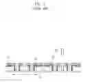
FIG. 5 illustrates a packaged multi-chip integrated circuit device including a package enclosure 274, a package substrate 272 and lower and upper integrated circuit chips 250—b and 250—t within a multi-chip stack 250′. The package substrate 272 is illustrated as including filled PCB vias 273. These filled vias transfer signals from upper conductive patterns 276 to lower conductive patterns 275 and vice versa. As illustrated, solder balls 271 may be mounted on the lower conductive patterns 275. The illustrated via holes 215 are filled with rerouting conductors 221. These rerouting conductors 221, which extend through the lower and upper integrated circuit chips 250—b and 250—t, include interchip connection bumps 277 (e.g., solder bumps). The illustrated pair of rerouting conductors 221 may pass separate chip select signals to a pair of integrated circuit devices in the upper integrated circuit chip 250—t. Additional rerouting conductors (not shown in FIG. 5) may also be used to pass separate chip select signals to a pair of integrated circuit devices in the lower integrated circuit chip 250—b. The use of four separate rerouting conductors to provide four separate chip select signals to four integrated circuit devices within two chips (e.g., 250—b and 250—t) can be achieved using the via hole formation illustrated by FIG. 6. In FIG. 6, the via holes 215e may be used to provide separate chip select signals to the chip pads 212a associated with the first and second integrated circuit devices 250a and 250b within one chip (e.g., lower chip 250—b). The via holes 215f may also be used so that separate chip select signals may be routed through one chip (e.g., lower chip 250—b) to another chip (e.g., upper chip 250—t). Moreover, the via holes 215d may be used so that rerouting conductors 221 may be shared by a pair of adjacent devices 250a and 250b.
In the drawings and specification, there have been disclosed typical preferred embodiments of the invention and, although specific terms are employed, they are used in a generic and descriptive sense only and not for purposes of limitation, the scope of the invention being set forth in the following claims.
Claims
That which is claimed is:1. An integrated circuit chip, comprising:
a semiconductor substrate;
a first integrated circuit device extending adjacent a first side of said semiconductor substrate and having a first plurality of chip pads thereon;
a second integrated circuit device extending adjacent a second side of said semiconductor substrate and having a second plurality of chip pads thereon;
first and second pluralities of via holes extending through a portion of said semiconductor substrate located between the first and second integrated circuit devices;
a first plurality of rerouting conductors extending from corresponding ones of the first plurality of chip pads to corresponding ones of the first plurality of via holes; and
a second plurality of rerouting conductors extending from corresponding ones of the second plurality of chip pads to corresponding ones of the second plurality of via holes.
2. The integrated circuit chip of claim 1, wherein a first one of the first plurality of chip pads is a chip select pad and a first one of the second plurality of chip pads is a chip select pad; and wherein one of the first plurality of rerouting conductors is electrically connected to the first one of the first plurality of chip pads and the first one of the second plurality of chip pads.
3. The integrated circuit chip of claim 1, wherein a first one of the first plurality of chip pads is a chip select pad and a first one of the second plurality of chip pads is a chip select pad; and wherein one of the first plurality of rerouting conductors is electrically connected to the first one of the first plurality of chip pads and one of the second plurality of rerouting conductors is electrically connected to the first one of the second plurality of chip pads.
4. The integrated circuit chip of claim 1, further comprising a rerouting conductor electrically connecting one of the first plurality of chip pads to one of the second plurality of chip pads.
5. A packaged integrated circuit device, comprising:
a package substrate; and
a semiconductor chip mounted to said package substrate, said semiconductor chip comprising a semiconductor substrate having first and second integrated circuit devices at spaced locations therein and a plurality of filled via holes extending through the semiconductor substrate at respective locations extending between the first and second integrated circuit devices.
6. The device of claim 5, wherein the plurality of filled via holes do not extend between any of the first and second integrated circuit devices and an edge of said semiconductor chip.
7. The device of claim 5, further comprising a first plurality of chip pads extending on a surface of said semiconductor chip and located in a space between the first integrated circuit device and the plurality of filled via holes.
8. The device of claim 7, further comprising a second plurality of chip pads extending on a surface of said semiconductor chip and located in a space between the second integrated circuit device and the plurality of filled via holes.
9. The device of claim 8, wherein one of first plurality of chip pads is a first chip select pad; wherein one of the second plurality of chip pads is a second chip select pad; wherein one of the plurality of filled via holes is associated with a first rerouting conductor connected to the first chip select pad; and wherein another one of the plurality of filled via holes is associated with a second rerouting conductor connected to the second chip select pad.
10. A packaged integrated circuit device, comprising:
a first semiconductor chip having first and second integrated circuit devices therein and a first plurality of via holes extending through said first semiconductor chip;
a second semiconductor chip mounted on said first semiconductor chip, said second semiconductor chip having third and fourth integrated circuit devices therein and a second plurality of via holes extending through said second semiconductor chip;
a first rerouting conductor that extends through said first semiconductor chip and is electrically connected to a chip select pad associated with the first integrated circuit device; and
a second rerouting conductor that extends through said first semiconductor chip and is electrically connected to a chip select pad associated with the second integrated circuit device.
11. The packaged integrated circuit device of claim 10, further comprising:
a third rerouting conductor that extends through said first and second semiconductor chips and is electrically connected to a chip select pad associated with the third integrated circuit device; and
a fourth rerouting conductor that extends through said first and second semiconductor chips and is electrically connected to a chip select pad associated with the fourth integrated circuit device.
12. The packaged integrated circuit device of claim 10, wherein the first and second rerouting conductors extend through first and second ones of the first plurality of via holes.
13. The packaged integrated circuit device of claim 11, wherein the first and second rerouting conductors extend through first and second ones of the first plurality of via holes; and wherein the third and fourth rerouting conductors extend through third and fourth ones of the first plurality of via holes.
14. The packaged integrated circuit device of claim 13, wherein the third and fourth rerouting conductors extend through first and second ones of the second plurality of via holes.
15. The packaged integrated circuit device of claim 14, wherein the third rerouting conductor comprises a connector bump that extends between the first and second semiconductor chips.
16. A packaged integrated circuit device, comprising:
a package substrate; and
a multi-chip stack of integrated circuit devices on said package substrate, said multi-chip stack comprising at least one chip-select rerouting conductor extending from said package substrate to a chip pad on an upper one of the chips in the multi-chip stack and passing through a first via hole in a lower one of the chips in the multi-chip stack.
17. The packaged integrated circuit device of claim 16, wherein the lower one of the chips in the multi-chip stack comprises first and second integrated circuit devices therein that are separated by a plurality of via holes including the first via hole.
Images & Drawings included:


Sources:
- United States Patent and Trademark Office - verify current appl. status at the USPTO↗
Recent applications in this class:
- » 20250293121 2025-09-18
LOW COST EMBEDDED INTEGRATED CIRCUIT DIES - » 20250285942 2025-09-11
THROUGH SUBSTRATE VIA (TSV) VALIDATION STRUCTURE FOR AN INTEGRATED CIRCUIT AND METHOD TO FORM THE TSV VALIDATION STRUCTURE - » 20250285941 2025-09-11
LAYOUT METHOD AND MEMORY MACRO INCLUDING THROUGH-SILICON VIA - » 20250285940 2025-09-11
PRINTED CIRCUIT BOARD - » 20250266325 2025-08-21
Semiconductor Device Having Backside Interconnect Structure on Through Substrate Via - » 20250266324 2025-08-21
MANUFACTURING METHOD OF SEMICONDUCTOR PACKAGE - » 20250266323 2025-08-21
SEMICONDUCTOR DEVICE AND METHOD - » 20250266322 2025-08-21
SUBSTRATE COMPRISING VIAS AND ASSOCIATED MANUFACTURING METHODS - » 20250266321 2025-08-21
SEMICONDUCTOR DEVICE AND METHOD FOR MANUFACTURING THE SAME - » 20250259914 2025-08-14
SEMICONDUCTOR PACKAGE AND METHOD OF MANUFACTURING THE SAME
Recent applications for this Assignee:
- » 20250175180 2025-05-29
INPUT BUFFER CIRCUIT AND POWER MANAGEMENT INTEGRATED CIRCUIT INCLUDING THE SAME - » 20250125998 2025-04-17
HYBRID SOURCE-SERIES TERMINATION DRIVER WITH CONSTANT OUTPUT SWING - » 20250117337 2025-04-10
PRE-FETCHING ADDRESS TRANSLATION FOR COMPUTATION OFFLOADING - » 20250069538 2025-02-27
DISPLAY DEVICE AND DRIVING METHOD THEREOF - » 20240430140 2024-12-26
RECEIVERS AND SEMICONDUCTOR MEMORY DEVICES INCLUDING THE SAME - » 20240414035 2024-12-12
RECEIVER, OPERATION METHOD THEREOF, AND MEMORY DEVICE - » 20240380824 2024-11-14
METHODS AND SYSTEMS TO PUSH NOTIFICATION MESSAGES IN SEAL NOTIFICATION MANAGEMENT SERVICE - » 20240377988 2024-11-14
MEMORY DEVICE AND OPERATION METHOD THEREOF - » 20240371417 2024-11-07
Semiconductor memory devices - » 20240348366 2024-10-17
METHOD AND APPARATUS FOR DECODING POLARIZATION-ADJUSTED CONVOLUTIONAL CODE BY USING LIST VITERBI ALGORITHM ADJUSTING LIST SIZE DYNAMICALLY