Dispensable capacitor manufacturing process
US20060228817A1
2006-10-12
11/100,449
2005-04-07
Abstract:
A dispensable capacitor manufacturing process allowing easier process, capacity correction facilitating, and reduced production cost essentially involves dispensing conductive epoxy between two soldering points on a PCB, use of laser to cut on the surface of solidified epoxy spaced grooves in different forms, heated dielectric material then permeated, insulation layer coated on surface after solidification, test and correction to constitute capacitor.
Interested in similar patents?
Get notified when new applications in this technology area are published.
Classification:
H05K1/162 » CPC main
Printed circuits incorporating printed electric components, e.g. printed resistor, capacitor, inductor incorporating printed capacitors
H05K1/162 » CPC main
Printed circuits incorporating printed electric components, e.g. printed resistor, capacitor, inductor incorporating printed capacitors
H01G4/005 » CPC further
Fixed capacitors; Processes of their manufacture; Details Electrodes
G01R31/016 » CPC further
Arrangements for testing electric properties; Arrangements for locating electric faults; Arrangements for electrical testing characterised by what is being tested not provided for elsewhere; Subjecting similar articles in turn to test, e.g. "go/no-go" tests in mass production; Testing objects at points as they pass through a testing station; Testing passive components Testing of capacitors
H05K1/095 » CPC further
Printed circuits; Details; Use of materials for the conductive, e.g. metallic pattern; Dispersed materials, e.g. conductive pastes or inks for polymer thick films, i.e. having a permanent organic polymeric binder
H05K1/095 » CPC further
Printed circuits; Details; Use of materials for the conductive, e.g. metallic pattern; Dispersed materials, e.g. conductive pastes or inks for polymer thick films, i.e. having a permanent organic polymeric binder
H05K3/027 » CPC further
Apparatus or processes for manufacturing printed circuits in which the conductive material is applied to the surface of the insulating support and is thereafter removed from such areas of the surface which are not intended for current conducting or shielding the conductive material being removed by irradiation, e.g. by photons, alpha or beta particles
H05K2201/09236 » CPC further
Indexing scheme relating to printed circuits covered by; Shape and layout; Shape and layout details of conductors; Conductive traces Parallel layout
H05K2201/09236 » CPC further
Indexing scheme relating to printed circuits covered by; Shape and layout; Shape and layout details of conductors; Conductive traces Parallel layout
H05K2203/1453 » CPC further
Indexing scheme relating to apparatus or processes for manufacturing printed circuits covered by; Related to the order of processing steps Applying the circuit pattern before another process, e.g. before filling of vias with conductive paste, before making printed resistors
H01L21/20 IPC
Processes or apparatus adapted for the manufacture or treatment of semiconductor or solid state devices or of parts thereof; Manufacture or treatment of semiconductor devices or of parts thereof the devices having at least one potential-jump barrier or surface barrier, e.g. PN junction, depletion layer or carrier concentration layer the devices having semiconductor bodies comprising elements of Group IV of the Periodic System or AB compounds with or without impurities, e.g. doping materials Deposition of semiconductor materials on a substrate, e.g. epitaxial growth solid phase epitaxy
G01R31/26 IPC
Arrangements for testing electric properties; Arrangements for locating electric faults; Arrangements for electrical testing characterised by what is being tested not provided for elsewhere Testing of individual semiconductor devices
Description
BACKGROUND OF THE INVENTION(a) Technical Field of the Invention
The present invention is related to a manufacturing process of dispensable capacitor, and more particularly, to a capacitor manufacturing process that is simplified, capacity correction facilitating, and allowing reduced production cost.
(b) Description of the Prior Art
As illustrated in FIGS. 1, and 2 of the accompanying drawings, the manufacturing process of the ceramic capacitor is generally available in the market and usually involves dispensing an electrode 11 on multiple ceramic green sheets 1 with one end of the electrode 11 staying closely to the lateral side of the ceramic green sheet while another end of the electrode 11 keeping a proper spacing from another lateral side of the ceramic green sheet 1 before stacking up those multiple ceramic green sheets 1 with the spaced sides between any two layered sheets 1 facing away from each other. Both lateral sides of the deck are then respectively provided each with a soldering end 12 to constitute a capacitor 100. However, this manufacturing process of the prior is found with the following flaws:
- 1. Complicated process, increased production cost, and higher percentage of nonconformity.
- 2. Capacity error prevents correction for the capacitor 100 since capacity of the electrode dispensed is preset.
- 3. Enormous manufacturing facilities required consumes too much space, slower return of investment on the machinery, thus less competitive.
The primary purpose of the present invention is to provide a dispensable capacitor manufacturing process that is simplified, allowing correction of capacity and reduced production cost. In the present invention, conductive epoxy is dispensed between two soldering points on a PCB to omit the soldering process as needed in the prior art. The conductive epoxy dispensed is heated up and solidified before the laser cut on the surface of the epoxy spaced grooves, then dielectric material is coated and solidified to be followed with test, correction and repeated testing. An insulation protection layer is coated on the top of the conductive epoxy and dielectric material to improve impact and thermal durability while promoting the binding property of the PCB. Furthermore, two layers of conductive epoxy may be dispensed for increased capacity.
The foregoing object and summary provide only a brief introduction to the present invention. To fully appreciate these and other objects of the present invention as well as the invention itself, all of which will become apparent to those skilled in the art, the following detailed description of the invention and the claims should be read in conjunction with the accompanying drawings. Throughout the specification and drawings, identical reference numerals refer to identical or similar parts.
Many other advantages and features of the present invention will become manifest to those versed in the art upon making reference to the detailed description and the accompanying sheets of drawings in which a preferred structural embodiment incorporating the principles of the present invention is shown by way of illustrative example.
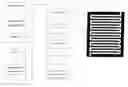
BRIEF DESCRIPTION OF THE DRAWINGSFIG. 1 is a perspective view of a ceramic capacitor of the prior art.
FIG. 2 is a sectional view of a cut-away from the ceramic capacitor of the prior art.
FIG. 3 is a process flow chart of the present invention.
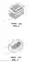
FIG. 4 is a schematic view showing a dispensable conductive epoxy of the present invention.
FIG. 5 is a sectional view showing the dispensable conductive epoxy of the present invention.
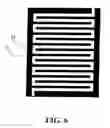
FIG. 6 is a schematic view showing a pattern of the laser cut on the conductive epoxy of the present invention.
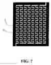
FIG. 7 is a schematic view showing another pattern of the laser cut on the conductive epoxy of the present invention.
DETAILED DESCRIPTION OF THE PREFERRED EMBODIMENTSThe following descriptions are of exemplary embodiments only, and are not intended to limit the scope, applicability or configuration of the invention in any way. Rather, the following description provides a convenient illustration for implementing exemplary embodiments of the invention. Various changes to the described embodiments may be made in the function and arrangement of the elements described without departing from the scope of the invention as set forth in the appended claims.
Referring to FIGS. 3 through 7, a dispensable capacitor manufacturing process of the present invention is essentially comprised of the following steps:
- A. Dispense a conductive epoxy 2 between two soldering points 31, 32 on a PCB 3 as illustrated in FIGS. 4 and 5.
- B. The dispensed conductive epoxy 2 is heated up and solidified.
- C. Laser cut on the surface of the solidified conductive epoxy 2 groove 21 in continuous zigzag shaped pattern as illustrated in FIGS. 6 and 7.
- D. Coat dielectric material (related to an epoxy with high insulation) on the conductive epoxy 2 after the cut, then solidified. In case of smaller spacing of the groove 21 cut in Step C, the dielectric materials must be heated up and dispensed by permeation, and air bulbs in the dielectric material are removed in a vacuum environment to get more consistent capacity.
- E. Run the capacity test, followed with later cut to change the capacity as required before repeating the test.
- F. Coat an insulation layer (epoxy) on the dielectric material for protection to improve impact and thermal durability while promoting the binding strength of the PCB (since the binding strength between epoxy and PCB soldering point is comparatively poor).
- G. The capacitor on the PCB soldering points is completed.
In addition to the single capacitor provided between two soldering points 31, 32 on the PCB, the capacitor is directly provided on any insulation substrate with sufficient mechanical strength without the soldering process as required in the prior art. Upon the completion of the first layer of conductive epoxy laser cut and coated with the dielectric material, a second layer conductive epoxy may be dispensed to form a double-layer structure for increased capacity and scope of applications.
It will be understood that each of the elements described above, or two or more together may also find a useful application in other types of methods differing from the type described above.
While certain novel features of this invention have been shown and described and are pointed out in the annexed claim, it is not intended to be limited to the details above, since it will be understood that various omissions, modifications, substitutions and changes in the forms and details of the device illustrated and in its operation can be made by those skilled in the art without departing in any way from the spirit of the present invention.
Claims
I claim:1. A dispensable capacitor manufacturing process includes the following steps:
Dispense conductive epoxy between two soldering points on a PCB.
Solidify the conductive epoxy dispensed in Step a.
Laser cut on the solidified conductive epoxy continuous zigzag shaped grooves.
Coat on the conductive epoxy after cut the dielectric material and left solidified.
Run the capacity test, correct, and repeat the test to come up with a finished product of capacitor.
Finally, coat insulation protection layer on the capacitor.
2. The dispensable capacitor manufacturing process of claim 1, wherein the conductive epoxy dispensed between two soldering points on the PCB is heated and solidified.
3. The dispensable capacitor manufacturing process of claim 1, wherein the dielectric material is removed with air bulbs, heated and dispensed in permeation fashion to the conductive epoxy in a vacuum environment in case of smaller spacing between grooves cut on the conductive epoxy.
4. The dispensable capacitor manufacturing process of claim 1, wherein a double-layer dispensable capacitor is made by applying a second layer of the conductive epoxy after the first layer of the conductive epoxy is solidified after the cut and permeated with the heated dielectric material.
Images & Drawings included:


Sources:
- United States Patent and Trademark Office - verify current appl. status at the USPTO↗
Recent applications in this class:
- » 20250071902 2025-02-27
PRINTED CIRCUIT BOARD - » 20250040051 2025-01-30
CAPACITIVE ELEMENT, CIRCUIT CARRIER HAVING THE SAME AND FABRICATION METHOD THEREOF - » 20250008659 2025-01-02
PRINTED CIRCUIT BOARD - » 20240431029 2024-12-26
INTEGRATED ASSEMBLY AND INTEGRATED POWER CONVERTER MODULE - » 20240224426 2024-07-04
WIRING SUBSTRATE - » 20230371181 2023-11-16
CIRCUIT BOARD SYSTEMS AND METHODS - » 20230319997 2023-10-05
CAPACITOR IN A SUBSTRATE VIA - » 20220369461 2022-11-17
Automatic trimming of a PCB-based LC circuit - » 20220053644 2022-02-17
Passive device packaging structure embedded in glass medium and method for manufacturing the same - » 20210219430 2021-07-15
Electronic component and its manufacturing method