Multiple-wavelength light emitting diode and its light emitting chip structure
US20060231847A1
2006-10-19
11/106,443
2005-04-15
Abstract:
The present invention discloses a multiple-wavelength light emitting diode that includes a fluorescent layer with a predetermined wavelength disposed at the bottom of the light emitting diode, such that a light emitting chip can be fixed onto a carrier and connected in parallel with the circuit of the light emitting chip by a gold wire. The light emitting chip is packaged by a package material to constitute a light emitting diode capable of combining the light source of the light emitting chip with the wavelength of the fluorescent layer, so as to produces the desired light color.
Inventors:
- MING-SHUN LEE 24 🇹🇼 TAIPEI, Taiwan
- Chang-Wei Ho 3 🇹🇼 Taipei, Taiwan
- Ping-Ru Sung 9 🇹🇼 Taipei, Taiwan
Interested in similar patents?
Get notified when new applications in this technology area are published.
Classification:
H01L33/505 » CPC main
Semiconductor devices with at least one potential-jump barrier or surface barrier specially adapted for light emission; Processes or apparatus specially adapted for the manufacture or treatment thereof or of parts thereof; Details thereof characterised by the semiconductor body packages; Wavelength conversion elements characterised by the shape, e.g. plate or foil
H01L24/32 » CPC further
Arrangements for connecting or disconnecting semiconductor or solid-state bodies; Methods or apparatus related thereto; Means for bonding being attached to, or being formed on, the surface to be connected, e.g. chip-to-package, die-attach, "first-level" interconnects; Manufacturing methods related thereto; Layer connectors, e.g. plate connectors, solder or adhesive layers; Manufacturing methods related thereto; Structure, shape, material or disposition of the layer connectors after the connecting process of an individual layer connector
H01L33/501 » CPC further
Semiconductor devices with at least one potential-jump barrier or surface barrier specially adapted for light emission; Processes or apparatus specially adapted for the manufacture or treatment thereof or of parts thereof; Details thereof characterised by the semiconductor body packages; Wavelength conversion elements characterised by the materials, e.g. binder
H01L33/60 » CPC further
Semiconductor devices with at least one potential-jump barrier or surface barrier specially adapted for light emission; Processes or apparatus specially adapted for the manufacture or treatment thereof or of parts thereof; Details thereof characterised by the semiconductor body packages; Optical field-shaping elements Reflective elements
H01L2224/73265 » CPC further
Indexing scheme for arrangements for connecting or disconnecting semiconductor or solid-state bodies and methods related thereto as covered by; Means for bonding being of different types provided for in two or more of groups; Location after the connecting process on different surfaces Layer and wire connectors
H01L2224/83385 » CPC further
Indexing scheme for arrangements for connecting or disconnecting semiconductor or solid-state bodies and methods related thereto as covered by; Methods for connecting semiconductor or other solid state bodies using means for bonding being attached to, or being formed on, the surface to be connected using a layer connector; Bonding interfaces outside the semiconductor or solid-state body Shape, e.g. interlocking features
H01L2224/8592 » CPC further
Indexing scheme for arrangements for connecting or disconnecting semiconductor or solid-state bodies and methods related thereto as covered by; Methods for connecting semiconductor or other solid state bodies using means for bonding being attached to, or being formed on, the surface to be connected using a wire connector; Post-treatment of the connector or wire bonding area Applying permanent coating, e.g. protective coating
H01L2924/15153 » CPC further
Indexing scheme for arrangements or methods for connecting or disconnecting semiconductor or solid-state bodies as covered by; Details of package parts other than the semiconductor or other solid state devices to be connected; Die mounting substrate; Shape the die mounting substrate comprising a recess for hosting the device
H01L2924/00014 » CPC further
Indexing scheme for arrangements or methods for connecting or disconnecting semiconductor or solid-state bodies as covered by; Technical content checked by a classifier the subject-matter covered by the group, the symbol of which is combined with the symbol of this group, being disclosed without further technical details
H01L2924/12041 » CPC further
Indexing scheme for arrangements or methods for connecting or disconnecting semiconductor or solid-state bodies as covered by; Details of semiconductor or other solid state devices to be connected; Device type; Passive devices, e.g. 2 terminal devices; Optical Diode LED
H01L2924/00 » CPC further
Indexing scheme for arrangements or methods for connecting or disconnecting semiconductor or solid-state bodies as covered by
H01L31/12 IPC
Semiconductor devices sensitive to infra-red radiation, light, electromagnetic radiation of shorter wavelength or corpuscular radiation and specially adapted either for the conversion of the energy of such radiation into electrical energy or for the control of electrical energy by such radiation; Processes or apparatus specially adapted for the manufacture or treatment thereof or of parts thereof; Details thereof structurally associated with, e.g. formed in or on a common substrate with, one or more electric light sources, e.g. electroluminescent light sources, and electrically or optically coupled thereto
Description
BACKGROUND OF THE INVENTION1. Field of the Invention
The present invention relates to a color light performance technology of a light emitting diode, and more particularly to a light emitting diode and its light emitting chip structure capable of producing correct light colors and enhance brightness performance effectively.
2. Description of the Related Art
In general, a basic structure of a light emitting diode includes a related package material to package a light emitting chip, and a gold wire used to electrically connect the light emitting chip with related circuits. The light emitting chip produces a light source after the light emitting chip is electrically connected. The light source is projected outward from the package material and further combined with the wavelength of a fluorescent material in the package material to produce a desired light color.
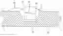
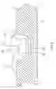
Referring to FIG. 1, the present common traditional light emitting diode structure directly adopts a substrate 10 as the carrier of a light emitting chip 20. The light emitting diode of this type implants a recessed base 11 into the surface of the substrate 10, and the recessed base 11 fixes the light emitting chip 20 in position and provides a space for filling the package material 30. In practical applications, a bonding material 40 is coated between the light emitting chip 20 and the substrate 10 (or a carrier with similar function) to achieve the purpose of fixing the light emitting chip 20. However, such arrangement implants some regions at the bottom of the light emitting chip 20 into the bonding material 40, and thus reducing the overall brightness performance of the light emitting diode. Furthermore, it is not easy to control the composition of the bonding material 40, the coating area and the coating quantity, although the bonding material 40 is mixed with a fluorescent material to combine the light source of the light emitting chip with the wavelength of the fluorescent material to produce expected light colors, and thus it is unable to precisely control the quality of light colors for the overall performance of the light emitting diode.
SUMMARY OF THE INVENTIONIn view of the foregoing shortcomings of the prior art, the inventor of the present invention based on years of experience in the related field to conduct extensive researches and experiments to overcome the aforementioned shortcomings and finally invented the present invention.
It is a primary objective of the present invention to provide a multiple-wavelength light emitting diode comprising a fluorescent layer with a predetermined wavelength disposed at the bottom of the light emitting diode, such that a light emitting chip can be fixed onto a carrier and connected in parallel with the circuit of the light emitting chip. The light emitting chip is packaged by a package material to constitute a light emitting diode that combines the light source of the light emitting chip with the wavelength of the fluorescent layer, so as to produces the desired light color. Since the fluorescent layer is fixed onto the bottom of the light emitting diode in advance, therefore the coating area and the coating quantity can be controlled effectively and the quality of light color produced by the fluorescent layer can be controlled precisely. Even more, a reflective material installed at the lowest fluorescent layer under the light emitting chip can effectively enhance the brightness performance of the light emitting diode.
BRIEF DESCRIPTION OF THE DRAWINGSFIG. 1 is a cross-sectional view of the structure of a prior art light emitting diode;
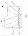
FIG. 2 is a perspective view of a light emitting diode according to a first preferred embodiment of the present invention;
FIG. 3 is a cross-sectional view of a light emitting diode according to a first preferred embodiment of the present invention;
FIG. 4 is a cross-sectional view of a light emitting diode according to a second preferred embodiment of the present invention;
FIG. 5 is a cross-sectional view of a light emitting diode according to a third preferred embodiment of the present invention;
FIG. 6 is a cross-sectional view of a light emitting diode according to a fourth preferred embodiment of the present invention;
FIG. 7 is a cross-sectional view of a light emitting diode according to a fifth preferred embodiment of the present invention; and
FIG. 8 is a cross-sectional view of a light emitting diode according to an eighth preferred embodiment of the present invention.
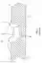
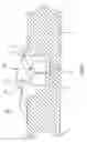
DETAILED DESCRIPTION OF THE PREFERRED EMBODIMENTSThe multiple-wavelength light emitting diode in accordance with the present invention provides a light emitting diode and its light emitting chip structure capable of producing a correct light color and effectively enhancing the brightness performance. In FIG. 2, the light emitting chip 20 includes a fluorescent layer 50 having a predetermined wavelength and disposed at the bottom of the light emitting chip 20, and the fluorescent layer 50 could be made of a single fluorescent power or made by mixing two or more fluorescent powders according to a predetermined proportion. In FIG. 3, the light emitting chip 20 is fixed into a predetermined space (or a carrier having a similar function) on the substrate 10 and the circuit of the light emitting chip 20 is connected in parallel by a gold wire 60. The light emitting chip 20 is packaged by a package material 30, so that the light source of the light emitting chip 20 can be combined with the wavelength of the fluorescent layer 50, so as to produce the expected light color.
Since the fluorescent layer 50 is fixed onto the bottom of the light emitting chip 20 in advance, therefore the coating area and the coating quantity can be controlled effectively and the quality of the light color produced by the fluorescent layer can be controlled precisely.
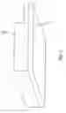
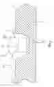
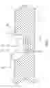
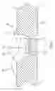
In practical applications, the multi-wavelength light emitting diode in accordance with the present invention is shown in FIG. 4. A plurality of fluorescent layers 50 having a predetermined wavelength is installed at the bottom of each light emitting chip 29 to constitute the combination of multi-wavelengths to produce the expected light color. Of course, a plurality of light emitting chips 20 could be installed in a light emitting diode as shown in FIG. 5, and a fluorescent layer 50 having a predetermined wavelength is installed at the bottom of each light emitting chip 20 or a fluorescent material having a predetermined wavelength is mixed in a predetermined proportion into the package material 30, so as to constitute more combinations of multiple wavelengths and produce the expected light color. Even more, a reflective material 70 is installed at the lowest fluorescent layer 50 under the light emitting chip 20 as shown in FIG. 6 to enhance the brightness performance of the light emitting diode, and the reflective material 70 is a natural crystal in the shape of a slab disposed at the bottom of the fluorescent layer 50 or a natural crystal having predetermined reflective lines on its surface as shown in FIG. 7. Of course, the reflective material 70 could have reflective particles directly mixed into the fluorescent layer 50 to project the light source of the light emitting diode in a predetermined direction, so as to enhance the brightness performance of the light emitting diode.
In summation of the above description, the present invention provides light emitting diode and its light emitting chip structure capable of producing a correct light color and effectively enhancing the brightness performance, and herein complies with the patent application requirements and is submitted for patent application. However, the description and its accompanied drawings are used for describing preferred embodiments of the present invention, and it is to be understood that the invention is not limited thereto. To the contrary, it is intended to cover various modifications and similar arrangements and procedures, and the scope of the appended claims therefore should be accorded the broadest interpretation so as to encompass all such modifications and similar arrangements and procedures.
Claims
What is claimed is:1. A chip, comprising:
a fluorescent layer, having a predetermined wavelength and disposed at the bottom of a light emitting chip.
2. A chip, comprising:
at least two fluorescent layers, having a predetermined wavelength and disposed at the bottom of a light emitting chip; and
a reflective material, disposed at the bottom of the lowest layer of said fluorescent layers.
3. The chip of claim 2, wherein said reflective material is a natural crystal having predetermined reflective lines on its surface or in the shape of a slab.
4. The chip of claim 2, wherein said reflective material includes reflective particles mixed in said fluorescent layer.
5. The chip of claim 1, wherein said fluorescent layer is made of a single fluorescent powder or made by mixing at least two fluorescent powders according to a predetermined proportion.
6. A light emitting diode, comprising:
at least one light emitting chip, installed on a carrier;
a gold wire, for connecting a circuit of said light emitting chip in parallel;
a package material, for packaging said light emitting chip; and
a fluorescent layer, having a predetermined wavelength and disposed at the bottom of said each light emitting chip.
7. The light emitting diode of claim 6, wherein said package material is mixed in a predetermined proportion with at least one fluorescent material having a predetermined wavelength.
8. A light emitting diode, comprising:
at least one light emitting chip, installed on a carrier;
a gold wire, for connecting a circuit of said light emitting chip in parallel;
a package material, for packaging said light emitting chip;
a fluorescent layer, having a predetermined wavelength and disposed at the bottom of said each light emitting chip; and
a reflective material disposed at the lowest fluorescent layer of said light emitting chip.
9. The light emitting diode of claim 8, wherein said reflective material is a natural crystal in the shape of a slab or having predetermined lines on the surface of said natural crystal.
10. The light emitting diode of claim 8, wherein said reflective material comprises reflective particles mixed in said fluorescent layer.
Images & Drawings included:
Sources:
- United States Patent and Trademark Office - verify current appl. status at the USPTO↗
Recent applications in this class:
- » 20250072176 2025-02-27
DISPLAY DEVICE - » 20250072175 2025-02-27
DISPLAY DEVICE - » 20250063865 2025-02-20
LIGHT SOURCE MODULE AND BACKLIGHT UNIT HAVING THE SAME - » 20250056936 2025-02-13
SIDE EMITTING LED PACKAGE WITH BEVEL LIGHT EMITTING SURFACE - » 20250056935 2025-02-13
DISPLAY DEVICE - » 20250040315 2025-01-30
TRANSPARENT DISPLAY APPARATUS - » 20250031495 2025-01-23
RADIATION-EMITTING COMPONENT AND METHOD FOR PRODUCING A RADIATION-EMITTING COMPONENT - » 20250022990 2025-01-16
DISPLAY DEVICE USING SEMICONDUCTOR LIGHT-EMITTING ELEMENT - » 20250015238 2025-01-09
WAVELENGTH CONVERSION SHEET-USE FILM, WAVELENGTH CONVERSION SHEET, BACKLIGHT, AND DISPLAY DEVICE - » 20250015237 2025-01-09
DISPLAY MODULE AND DISPLAY DEVICE