GaN semiconductor devices with A1N buffer grown at high temperature and method for making the same
US20060249741A1
2006-11-09
11/410,995
2006-04-25
Abstract:
A method for growing high-quality single crystal III-V compound semiconductor layers of nitrides on a substrate that has a large lattice mismatch including first forming an AIN layer on a substrate, and then forming a GaN layer on the AIN layer.
Interested in similar patents?
Get notified when new applications in this technology area are published.
Classification:
C30B25/183 » CPC main
Single-crystal growth by chemical reaction of reactive gases, e.g. chemical vapour-deposition growth; Epitaxial-layer growth characterised by the substrate being provided with a buffer layer, e.g. a lattice matching layer
C30B29/406 » CPC further
Single crystals or homogeneous polycrystalline material with defined structure characterised by the material or by their shape; Inorganic compounds or compositions; AB compounds wherein A is B, Al, Ga, In or Tl and B is N, P, As, Sb or Bi; A-nitrides Gallium nitride
H01L21/0242 » CPC further
Processes or apparatus adapted for the manufacture or treatment of semiconductor or solid state devices or of parts thereof; Manufacture or treatment of semiconductor devices or of parts thereof; Forming layers; Forming inorganic semiconducting materials on a substrate; Substrates; Materials Crystalline insulating materials
H01L33/007 » CPC further
Semiconductor devices with at least one potential-jump barrier or surface barrier specially adapted for light emission; Processes or apparatus specially adapted for the manufacture or treatment thereof or of parts thereof; Details thereof; Processes for devices with an active region comprising only III-V compounds with a substrate not being a III-V compound comprising nitride compounds
H01L33/00 IPC
Semiconductor devices with at least one potential-jump barrier or surface barrier specially adapted for light emission; Processes or apparatus specially adapted for the manufacture or treatment thereof or of parts thereof; Details thereof
Description
CLAIM FOR PRIORITYPriority is hereby claimed to U.S. Provisional Patent Application Ser. No. 60/674,595 filed on Apr. 25, 2005.
BACKGROUNDThis disclosure relates to various GaN semiconductor devices, including those with a selective etching low-temperature buffer, and related methods for growing single crystal III-V compound semiconductor layers, including those where such layers include nitrides.
Generally, most GaN-based optoelectronics are grown on sapphire substrates. However, the lattice-mismatch between GaN and sapphire is extremely large, such as up to 13.8%, hence, GaN is usually grown using a thin (normally 25-30 nm) polycrystalline AIN or GaN nucleation layer (NL) grown at low temperature (normally 400-650° C.). After the NL is grown, the consequent GaN layer is grown at a high temperature (normally over 1000° C.) prior to growth of any device structures, and is called the “HT GaN layer”. This HT GaN layer growth is generally thought to proceed via an islanding and coalescence mechanism. That means the initial growth of the HT GaN layer appears in the form of islands, each with a truncated hexagonal pyramid shape. The islands coalesce with each other as growth continues. Finally, the HT GaN layer becomes flat. Without use of a low temperature buffer layer on the substrate, GaN cannot be deposited on the sapphire substrate at high temperature. Presently this is a standard growth procedure for all GaN-based optoelectronic grown on sapphire substrates. However, due to the thin low temperature NL, a high density of dislocations in the consequent GaN layer grown at a high temperature is introduced. Generally, the dislocation density is over than 108/cm2, even up to 1010/cm2, which makes the performance of GaN-based optoelectronics degrade, for example, GaN-based violet/blue laser diodes grown on sapphire substrate can not work in continuous wave (cw) mode or work in cw mode only with a short lifetime. Such lasers have a dramatically decreased dislocation density when observed by transmission electron microscopy (TEM). In order to construct such lasers, it is necessary to decrease dislocation density of the GaN layer.
In order to increase the crystal quality of GaN-based optoelectronics on sapphire substrates, the low temperature NL should be avoided.
For more background, the reader is directed to the following references which are hereby incorporated by reference:
-
- 1. I. Akasaki, H. Amano, Y. Koide, K Hiramatsu and N. Sawaki, J. Cryst. Growth 98, 209 (1989).
- 2. S. Nakamura, Jpn. J. Appl. Phys., Part 2 30, L1705 (1991).
- 3. T. Wang, D. Nakagawa, H. B. Sun, H. X. Wang, J. Bai, S. Sakai and H. Misawa, Appl. Phys. Lett. 76, 2220 (2000).
- 4. T. Wang, Y. Morishima, N. Naoi and S. Sakai, J. Cryst. Growth 213, 188 (2000).
It is desired to provide a method for growing one or more high-quality single crystal III-V compound semiconductor layers of nitrides on a substrate that has a large lattice mismatch compared with GaN, such as sapphire.
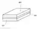
BRIEF DESCRIPTION OF THE DRAWINGSFIG. 1 is a cross-sectional view of a conventional GaN on a sapphire substrate.
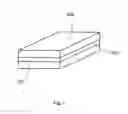
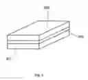
FIG. 2 is schematic illustration of growth procedure.
FIG. 3 is a (0002) XRD rocking curve of 0.7 micrometer AIN.
FIG. 4 is (0002) XRD rocking curves of a GaN layer compared to conventional GaN layer grown using prior art technology.
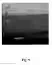
FIG. 5 is a cross-section TEM image of a GaN layer.
DETAILED DESCRIPTIONReferring to FIG. 1, conventional growth of GaN on a sapphire substrate is depicted. A sapphire substrate 101 of known prior art configuration is provided. For processing in an MOCVD system, the substrate 101 was initially annealed, such in as ambient H2, at high temperature such as higher than 1000° C. Then the temperature is decreased to a lower level such as 450° C. to 600° C. for the growth of low temperature (LT) nucleation layer (NL) 102. The nucleation layer is an appropriate material such as GaN or AIN. An example of appropriate thickness for the low temperature buffer layer is 20-35 nm. Thicker or thinner nucleation layer will lead to a degraded crystal quality. Then a several micrometer thick undoped GaN layer 103 is grown at a high temperature such 1000° C. to 1150° C.
Referring to FIG. 2, an example of the invention for growth of GaN on sapphire substrate with non-LT-NL approach is depicted. The substrate 201 is initially annealed, such in as ambient H2, at high temperature such as higher than 1000° C., which is same as the above description. The next procedure is different from above, namely, a layer of AIN 202 is grown directly on sapphire substrate at a temperature above 1000° C. instead of LT NL. The thickness of AIN layer can be larger than 40 nm and can be up to a few micrometers. The growth temperature for the growth of AIN can be greater than 1000° C., and V/III ratio can be from 500 to 30. The excellent crystal quality of AIN buffer can be seen from X-ray diffraction (XRD) (0002) rocking curves, which can sensitively evaluate the crystal quality. For example, the (0002) XRD rocking curve of 0.7 micrometer AIN grown using this procedure indicates that the full width at half maximal (FWHM) of XRD rocking curve is as narrow as about 59 arcsecs, as shown in FIG. 3. Afterwards, a normal GaN layer 203 with a few micrometers is subsequently grown on this high quality AIN layer at a temperature of over than 1000° C. The dislocation density in the part of the grown GaN layer on this AIN layer is reduced greatly using this technique compared to prior art techniques.
FIG. 4 shows the X-ray diffraction (XRD) (0002) rocking curves of GaN grown using the invented technique compared to conventional GaN using a low temperature thin nucleation layer, which can sensitively evaluate the crystal quality. This means that the narrow full width at half maximal (FWHM) of XRD rocking curve indicates a low dislocation density and high crystal quality. Normally, the FWHM of (0002) XRD rocking curve is larger than 250 arcsecs, while that of GaN grown using our invention is only 75 arcsec. This means that the crystal quality of GaN grown using the invention can be dramatically improved.
The improvement of the crystal quality can be further confirmed by TEM measurement. FIG. 5 shows the TEM image, in which the threading dislocation density of GaN layer is almost invisible, meaning that the dislocation density is below the TEM resolution, namely, the dislocation density of GaN layer is below 107/cm2. In contrast to it, the dislocation density of conventional GaN grown on sapphire substrate is generally above 108/cm2.
Based on such technology, a high performance InGaN/GaN-based LD, LED, AlGaN/GaN-based UV-LED, and GaN-based electron device can be also grown.
While the present invention has been described and illustrated in conjunction with a number of specific embodiments, those skilled in the art will appreciate that variations and modifications may be made without departing from the principles of the inventions as herein illustrated, described and claimed. The present invention may be embodied in other specific forms without departing from their spirit or characteristics. The described embodiments are to be considered in all respects as only illustrative, and not restrictive. The scope of the invention is, therefore, indicated by the appended claims, rather than the foregoing description. All changes that come within the meaning and range of equivalency of the claims are to be embraced within their scope.
Claims
1. A method for growing high-quality single crystal Ill-V compound semiconductor layers of nitrides on a substrate that has a large lattice mismatch comprising the steps of
annealing a sapphire substrate,
growing a layer of AIN on said sapphire substrate, and
forming a layer of GaN on said AIN layer.
2. A method as recited in claim 1 wherein said annealing step is performed in ambient H2.
3. A method as recited in claim 1 wherein said annealing step is performed at a temperature.
4. A method as recited in claim 1 greater than 1000° C.
5. A method as recited in claim 1 wherein said growing step takes place at a temperature greater than 1000° C.
6. A method as recited in claim 1 wherein said AIN layer has a thickness of more than 40 nm.
7. A method as recited in claim wherein said AIN layer has a thickness of not less than 1 micrometer.
8. A method as recited in claim 1 wherein said AIN layer has a V/III ration of from about 500 to about 30.
9. A method as recited in claim 1 wherein said forming step takes place at a temperature greater than 1000° C.
10. A method as recited in claim 1 wherein said GaN layer has a thickness of more than 1 micrometer.
11. A method as recited in claim 1 wherein said GaN layer has a reduced dislocation density.
12. A method as recited in claim 1 wherein a (0002) XRD rocking curve of 0.7 micrometer AIN grown using the method indicates that the full width at half maximal (FWHM) of the XRD rocking curve is about 59 arcsecs.
Images & Drawings included:
Sources:
- United States Patent and Trademark Office - verify current appl. status at the USPTO↗
Recent applications in this class:
- » 20250154682 2025-05-15
HETEROEPITAXIAL WAFER FOR THE DEPOSITION OF GALLIUM NITRIDE - » 20250101630 2025-03-27
HIGH-CHARACTERISTIC EPITAXIAL GROWTH SUBSTRATE AND METHOD FOR MANUFACTURING SAME - » 20250019861 2025-01-16
PROCESS FOR GROWING ACTIVE LAYERS IN SEQUENCE - » 20240401230 2024-12-05
COMPOSITE SUBSTRATE AND MANUFACTURING METHOD THEREOF - » 20240392472 2024-11-28
METHOD OF PHASE-TRANSITIONING THREE-DIMENSIONAL DIRAC SEMIMETAL INTO TWO-DIMENSIONAL WEYL SEMIMETAL AND SEMIMETAL THAT UNDERGOES PHASE TRANSITION BY THE SAME - » 20240229293 2024-07-11
PHASE STABILIZED GROWTH OF MONOCLINIC-GALLIUM OXIDE ON THERMALLY CONDUCTING MATERIALS - » 20240084479 2024-03-14
DYNAMIC HVPE OF COMPOSITIONALLY GRADED BUFFER LAYERS - » 20240044043 2024-02-08
METHOD FOR PRODUCING A MONOCRYSTALLINE LAYER OF LITHIUM NIOBATE BY TRANSFERRING A SEED LAYER OF YTTRIA-STABILIZED ZIRCONIA TO A SILICON CARRIER SUBSTRATE AND EPITAXIALLY GROWING THE MONOCRYSTALLINE LAYER OF LITHIUM NIOBATE AND SUBSTRATE FOR EPITAXIAL GROWTH OF A MONOCRYSTALLINE LAYER OF LITHIUM NIOBATE - » 20230257905 2023-08-17
LARGE-DIAMETER SUBSTRATE FOR GROUP-III NITRIDE EPITAXIAL GROWTH AND METHOD FOR PRODUCING THE SAME - » 20230250552 2023-08-10
BASE SUBSTRATE FOR GROUP III-V COMPOUND CRYSTALS AND PRODUCTION METHOD FOR SAME