Wafer dicing process for optical electronic packing
US20060286773A1
2006-12-21
11/328,094
2006-01-10
✅ Patent granted
US 7,294,559 B2
2007-11-13
-
-
Scott B. Geyer | Reema Patel
2026-01-10
Abstract:
A wafer dicing process for optical electronic packing is provided. The process includes: providing a first wafer (glass wafer) and a second wafer (interposer wafer); etching the second wafer to form a reference plane coordinate; laminating the first wafer on the second wafer, providing a third wafer (CMOS wafer); laminating the third wafer under the second wafer, cutting the first wafer by a first dicing saw according to the reference plane coordinate, dicing the third wafer by a second dicing saw to form a first reference axis and a second reference axis perpendicular with each other and to establish a backside dicing reference coordinate. The process not only can reduce wearing loss of the dicing saws but also ensure to form high quality cutting edges and a precise backside dicing reference coordinate.
Assignee:
- ADVANCED SEMICONDUCTOR ENGINEERING, INC. 1,972 🇹🇼 Kaohsiung, Taiwan
Interested in similar patents?
Get notified when new applications in this technology area are published.
Classification:
H01L21/78 » CPC main
Processes or apparatus adapted for the manufacture or treatment of semiconductor or solid state devices or of parts thereof; Manufacture or treatment of devices consisting of a plurality of solid state components formed in or on a common substrate or of parts thereof; Manufacture of integrated circuit devices or of parts thereof; Manufacture or treatment of devices consisting of a plurality of solid state components or integrated circuits formed in, or on, a common substrate with subsequent division of the substrate into plural individual devices
H01L21/67092 » CPC further
Processes or apparatus adapted for the manufacture or treatment of semiconductor or solid state devices or of parts thereof; Apparatus specially adapted for handling semiconductor or electric solid state devices during manufacture or treatment thereof; Apparatus specially adapted for handling wafers during manufacture or treatment of semiconductor or electric solid state devices or components ; Apparatus not specifically provided for elsewhere; Apparatus not specifically provided for elsewhere; Apparatus for manufacture or treatment Apparatus for mechanical treatment
H01L21/00 IPC
Processes or apparatus adapted for the manufacture or treatment of semiconductor or solid state devices or of parts thereof
H01L21/30 IPC
Processes or apparatus adapted for the manufacture or treatment of semiconductor or solid state devices or of parts thereof; Manufacture or treatment of semiconductor devices or of parts thereof the devices having at least one potential-jump barrier or surface barrier, e.g. PN junction, depletion layer or carrier concentration layer the devices having semiconductor bodies comprising elements of Group IV of the Periodic System or AB compounds with or without impurities, e.g. doping materials Treatment of semiconductor bodies using processes or apparatus not provided for in groups -
Description
BACKGROUND OF THE INVENTION1. Field of the Invention
The present invention relates to a wafer dicing process for optical electronic packing, and more particularly to a wafer dicing process for optical electronic packing, which elongates the lifetime of the dicing saws and forms high quality cutting plane and a precise backside dicing reference coordinate.
2. Description of the Prior Art
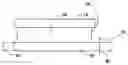
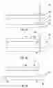
In the field of optical electronic packing, a package has to perform multiple functions. Therefore the structure of the package in wafer level packing possibly consists of several materials. FIG. 1A and FIG. 1B schematically illustrate a traditional wafer dicing process for optical electronic packing. The structure of the package contains three wafers with different materials and functions, including a first wafer p10 (glass wafer), a third wafer p30 (Complementary Metal-Oxide Semiconductor, COMS) wafer, and a second wafer p20 (interposer wafer) which separates the first wafer p10 a distance from the third wafer p30. These three wafers form a laminated structure for optical electronic packing. The traditional method to dice the packed wafer is cutting through by a single dicing saw p40. By using this method, the cutting plane of the wafer package is not smooth and forming a rough plane p31. It not only affects the cutting precision, but also increases the wearing rate of the dicing saw p40 by using this single dicing saw to cut through the laminated waters.
SUMMARY OF THE INVENTIONIn view of the foregoing, it is an object of the present invention to provide a wafer dicing process for optical electronic packing, which can ensure the quality of the reference plane coordinate and avoid cutting misalignment to damage the package due to the distorting axis of the reference coordinate.
According to one embodiment of the present invention, the wafer dicing process for optical electronic packing is including the following steps: providing a first wafer with a first upper surface and a first lower surface; providing a second wafer with a second upper surface and a second lower surface; etching the second wafer to form a first plane and a second plane perpendicular with each other and to establish a reference plane coordinate by them; laminating the first wafer on the second wafer, in which the second upper surface of the second wafer faces to the first lower surface of the first wafer; providing a third wafer having an active surface; laminating the third wafer under the second wafer, in which the active surface of the third wafer faces to the lower surface of the second wafer; dicing the first wafer by a first dicing saw from its upper surface according to the reference plane coordinate to reveal the third wafer; and dicing the third wafer by a second dicing saw according to the reference plane coordinate to form a first reference axis and a second reference axis perpendicular with each other and to establish a backside dicing reference coordinate.
In the previous process, the first wafer is a glass wafer and the first dicing saw is specified for cutting a glass wafer. The second wafer is adopted as an interposer wafer. The third wafer is a CMOS (Complementary Metal-Oxide Semiconductor) wafer and the second dicing saw is specified for cutting a CMOS wafer. The method for laminating the first and the second wafers is by hot-pressing as well as for laminating the second and the third wafers.
BRIEF DESCRIPTION OF THE DRAWINGSFIG. 1A and FIG. 1B schematically illustrate a conventional method to dice optical electronic wafer according to a reference coordinate.
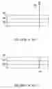
FIG. 2A and FIG. 2B are plane drawings schematically illustrating the formation of a reference coordinate on the second wafer according to one embodiment of the present invention.
FIG. 3A to FIG. 3F are cross-sectional-drawings schematically illustrating the process of dicing an optical electronic wafer according one embodiment of the present invention.
DESCRIPTION OF THE PREFERRED EMBODIMENTThe embodiment of this invention discloses a wafer dicing process for optical electronic packing and the detail description is as following. FIG. 2A and FIG. 2B schematically illustrates the method to form a reference coordinate on a second wafer 20. FIG. 2A shows the second wafer 20 which is usually taken as an interposer wafer in optical electronic packing. As shown in FIG. 2B, the wafer can be etched to form a first plane 23 and a second plane 24 which are perpendicular with each other, and a reference coordinate 25 can be established according to these two planes. Subsequently, the reference coordinate 25 can use for the following alignment on the wafer dicing process.
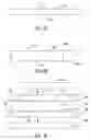
FIG. 3A to FIG. 3E schematically illustrates a wafer dicing process for optical electronic packing according to the embodiment of this invention. FIG. 3A shows a wafer 10 with a first upper surface 11 and a first lower surface 12, which is usually a glass wafer. FIG. 3B shows the second wafer with a second upper surface 21 and a second lower surface 22. And the details to form the reference coordinate 25 has described in the previous paragraph. First the first wafer 10 laminates with the second wafer 20, in which the first lower surface 12 of the first wafer 10 faces to the second upper surface 21 of the second wafer 20, and forming a wafer stack. A third wafer 30 with an active surface 31 is a CMOS (Complementary Metal-Oxide Semiconductor) wafer, in which the active surface 31 offers the function of input or output the electrical signals. The third wafer 30 is then laminated with the previous wafer stack to form an optical electronic wafer package as shown in FIG. 3C, in which the active surface 31 of the third wafer 30 faces to the second lower surface 22 of the second wafer.
Because the first wafer 10 is a transparent glass material, the reference coordinate 25 on the second wafer 20 can clearly monitor by looking through the first wafer 10. This enables to cut the first wafer 10 by a first dicing saw 40 from the first upper surface 11 to form planes and to reveal the third wafer 30 according to the reference coordinate 25 on the second wafer 20. Subsequently, the third wafer 30 is cut by a second dicing saw 50 to form a first reference axis 60 and a second reference axis 70 perpendicular with each other according to the reference axis of the reference coordinate 25. According to these two perpendicular first axis 60 and second axis 70 on the third wafer, the backside reference dicing coordinate 80 can be established and further use for dicing the wafer stack to form optical electronic chips.
In the previous embodiment of this invention, the process to cut the first wafer 10 and the third wafer 30 are belonging to two separating steps, so that the first dicing saw 40 for cutting a glass wafer can be chosen while cutting the first wafer 10 which is consisted of glass material, and similarly the second dicing saw 50 for cutting CMOS wafer can be chosen while cutting the third wafer 30, that can elongate the lifetime of the dicing saws.
In addition, the method for laminating the first wafer 10 with the second 20 and wafer stack with the third wafer 30 can adopt the hot-pressing process to attach them together according to the previous embodiment.
It is further understood by those skilled in the art that the foregoing description is a preferred embodiment of the disclosed process and that various changes and modifications may be made in the invention without departing from the spirit and scope therefore.
Claims
What is claimed is:1. A wafer dicing process for optical electronic packing, comprising:
providing a first wafer with a first upper surface and a first lower surface;
providing a second wafer with a second upper surface and a second lower surface;
etching said second wafer to form a first plane and a second plane perpendicular with each other and to establish a reference plane coordinate according to said first plane and said second plane;
laminating said first wafer on said second wafer, wherein said second upper surface of said second wafer facing to said first lower surface of said first wafer;
providing a third wafer with an active surface;
laminating said third wafer under said second wafer, wherein said active surface of said third wafer facing to said lower surface of said second wafer;
dicing said first wafer by a first dicing saw according to the position of said reference plane coordinate to reveal said third wafer; and
dicing said third wafer by a second dicing saw according to said reference plane coordinate to form a first reference axis and a second reference axis perpendicular with each other to establish a backside dicing reference coordinate
2. The wafer dicing process for optical electronic packing according to claim 1, wherein said first wafer is a glass wafer and said first dicing saw is specified for cutting said glass wafer.
3. The wafer dicing process for optical electronic packing according to claim 1, wherein said second wafer is an interposer wafer.
4. The wafer dicing process for optical electronic packing according to claim 1, wherein said third wafer is a CMOS (Complemetary Metal-Oxide Semiconductor) wafer and said second dicing saw is specified for cutting said CMOS wafer.
5. The wafer dicing process for optical electronic packing according to claim 1, wherein the method for laminating said first wafer with said second wafer is hot-pressing.
6. The wafer dicing process for optical electronic packing according to claim 1, wherein the method for laminating said second wafer with said third wafer is hot-pressing.
7. The wafer dicing process for optical electronic packing according to claim 1, wherein the method for forming said first plane and said second plane of said second wafer is an etching process.
Images & Drawings included:
Sources:
- United States Patent and Trademark Office - verify current appl. status at the USPTO↗
Recent applications in this class:
- » 20250293094 2025-09-18
METHOD FOR MANUFACTURING SEMICONDUCTOR DEVICE - » 20250293093 2025-09-18
METHOD OF MANUFACTURING SEMICONDUCTOR DEVICE - » 20250293092 2025-09-18
METHODS FOR SINGULATING SEMICONDUCTOR DIE FROM SILICON CARBIDE SUBSTRATES - » 20250285921 2025-09-11
METHOD FOR MANUFACTURING SEMICONDUCTOR DEVICE - » 20250273516 2025-08-28
MANUFACTURING METHOD OF ELECTRONIC PACKAGE - » 20250239492 2025-07-24
DEFORMATION CONTROL FOR DIE-TO-WAFER AND DIE-TO-DIE BONDING IN DEVICE MANUFACTURING - » 20250239491 2025-07-24
CHIP STRUCTURE AND METHOD OF MANUFACTURING THE SAME - » 20250239490 2025-07-24
DIE EDGE STRUCTURE FOR MOLDING COMPOUND FILLING AND THE METHODS OF FORMING THE SAME - » 20250233021 2025-07-17
DIE CLEANING SYSTEMS AND RELATED METHODS - » 20250226264 2025-07-10
FAN-OUT WAFER LEVEL PACKAGING OF SEMICONDUCTOR DEVICES
Recent applications for this Assignee:
- » 20250294670 2025-09-18
ELECTRONIC DEVICE - » 20250293221 2025-09-18
ELECTRONIC DEVICE - » 20250285950 2025-09-11
SEMICONDUCTOR DEVICE PACKAGE - » 20250282612 2025-09-11
PACKAGE STRUCTURE - » 20250273638 2025-08-28
SEMICONDUCTOR DEVICE PACKAGE INCLUDING STRESS BUFFERING LAYER - » 20250273531 2025-08-28
PACKAGE STRUCTURE - » 20250271555 2025-08-28
OPTOELECTRONIC STRUCTURE - » 20250266313 2025-08-21
SEMICONDUCTOR DEVICE PACKAGE AND METHOD OF MANUFACTURING THE SAME - » 20250260153 2025-08-14
ELECTRONIC DEVICE - » 20250259978 2025-08-14
SEMICONDUCTOR PACKAGE DEVICE AND METHOD OF MANUFACTURING THE SAME