Low noise amplifier with switch gain control
US20070057733A1
2007-03-15
11/223,344
2005-09-10
✅ Patent granted
US 7,301,403 B2
2007-11-27
-
-
Henry Choe
2026-02-09
Abstract:
This invention presents a low noise amplifier with switching gain control, comprising an amplifier having an impedance matching circuit a switch circuit, a signal amplifying branch circuit, a switch control circuit, a signal attenuating circuit and a current bias circuit, wherein the switch circuit controls signal amplifying or attenuating based on the high or low of an input signal level. This invention provides low noise, great dynamic range, increased system integration, and low power consumption. This invention is used for integrated circuit wireless communication system and RF preamplifiers for receiver.
Assignee:
- Comlent Technology, Inc. 1 🇨🇳 Shanghai, China
Interested in similar patents?
Get notified when new applications in this technology area are published.
Classification:
H03F3/45183 » CPC main
Amplifiers with only discharge tubes or only semiconductor devices as amplifying elements; Differential amplifiers with semiconductor devices only characterised by the way of implementation of the active amplifying circuit in the differential amplifier using MOSFET transistors as the active amplifying circuit Long tailed pairs
H03G1/0029 » CPC further
Details of arrangements for controlling amplification; Circuits characterised by the type of controlling devices operated by a controlling current or voltage signal the device being at least one of the amplifying solid state elements of the amplifier using FETs
H03G1/0088 » CPC further
Details of arrangements for controlling amplification; Circuits characterised by the type of controlling devices operated by a controlling current or voltage signal using discontinuously variable devices, e.g. switch-operated
H03F2203/45464 » CPC further
Indexing scheme relating to amplifiers with only discharge tubes or only semiconductor devices as amplifying elements covered by; Indexing scheme relating to differential amplifiers the CSC comprising one or more coils
H03F2203/45476 » CPC further
Indexing scheme relating to amplifiers with only discharge tubes or only semiconductor devices as amplifying elements covered by; Indexing scheme relating to differential amplifiers the CSC comprising a mirror circuit
H03F2203/45726 » CPC further
Indexing scheme relating to amplifiers with only discharge tubes or only semiconductor devices as amplifying elements covered by; Indexing scheme relating to differential amplifiers the LC comprising more than one switch, which are not cross coupled
H03F1/22 IPC
Details of amplifiers with only discharge tubes, only semiconductor devices or only unspecified devices as amplifying elements; Modifications of amplifiers to reduce detrimental influences of internal impedances of amplifying elements by use of cascode coupling, i.e. earthed cathode or emitter stage followed by earthed grid or base stage respectively
H03F3/04 IPC
Amplifiers with only discharge tubes or only semiconductor devices as amplifying elements with semiconductor devices only
Description
FIELD OF THE INVENTIONThe present invention relates to a low noise amplifier with switch gain control, and more particularly to a low noise amplifier in the receiving device of a wireless radio frequency system.
BACKGROUND OF THE INVENTIONIt is well known that the low noise amplifier is one of the essential components among wireless RF system devices. Commonly a low noise amplifier is used at the rear end of a wireless receiving device (e.g. antenna), to amplify very weak signal(s) received by the receiving device. The low noise amplifier requires a circuitry with low noise and high amplified ratio. Also when the input signal is strong it requires a more precise linearity and low gain.
FIG. 1 shows a block diagram of a prior art low noise amplifier having a switch parallel connected to the amplifier. The switch forms a bias circuit. The switch turns on when the input signal is low, forming an amplified gain. The switch turns off when the input signal is high, ensuring system linearity. However since a 50 Ω impedance is required in the system, energy consumption is high, and moreover the whole system cannot be integrated. Even when CMOS technique is used, a larger potential capacitor will be required, but with low isolation, which will induce a mismatched input signal when the switch turns off.
SUMMARY OF THE INVENTIONThe purpose of the present invention is to introduce a low noise amplifier with switch gain control, to raise the dynamic range of the wireless receiving device, increase the system integrated level, ensure the receiving sensitivities, and prevent saturation and clog occurring at rear end circuit of low noise amplifier.
The above purpose of present invention can be implemented as follows: A low noise amplifier with switch gain control consists of an amplifier having an impedance matching circuit connecting a switch circuit; the switch circuit delivers high or low signals into either signal amplifying path and signal attenuating path. The amplifier also connects to a current bias circuit.
The whole system dynamic range is improved when the present invention being utilized on receiver chip in wireless communication system, or on the front end chip in radio frequency (RF) receiver. The present invention can be implemented through either CMOS technique or BiCMOS technique. The signal path selection in present invention creates different gain. When the gain changes, the impedance on either input or output amplifier terminals remains the same. Specifically when input signal is low, the switch turns on, allowing the signal runs through signal amplifying circuit, while when the input signal is high, the switch turns off, allowing the signal runs through signal attenuating circuit. Such design is able to improve system gain, improve system linearity, lower noise, and ensure receipt sensitivity, while being fully integrated.
BRIEF DESCRIPTION OF THE DRAWINGSFIG. 1 is a circuit diagram of a prior art Low Noise Amplifier;
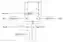
FIG. 2 is a schematic diagram of a Low Noise Amplifier with switch gain control in present invention;
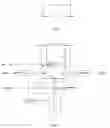
FIG. 3 is a circuit diagram of an attenuating circuit of a Low Noise Amplifier with switch gain control in present invention;
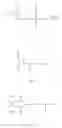
FIG. 4 is a circuit diagram of a current bias circuit of a Low Noise Amplifier with switch gain control in present invention;
FIG. 5 is a circuit diagram of a switch circuit of a Low Noise Amplifier with switch gain control in present invention;
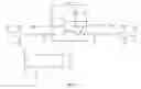
FIG. 6 is a detail circuit diagram of a Low Noise Amplifier with switch gain control in present invention.
Legend: Lg is an inductor; M1 is a voltage convertor (the NMOS transistor); LS is an inductor; M2 is a transistor; Ld is an inductor; M3 is a transistor; Rd is a resistor.
DETAILED DESCRIPTION OF THE PREFERRED EMBODIMENTDetail description of the drawings of the best embodiment is described as follows:
FIG. 6 shows an integrated Low Noise Amplifier with switch gain control. The Low Noise amplifier consists of an impedance matching circuit connecting a switch circuit, while the switch circuit delivers high or low signals into signal amplifying circuit and signal attenuating circuit. The amplifier also couples a current bias circuit.
As shown in FIG. 2, the impedance matching circuit consists of an inductor Lg, a voltage-current converter M1 and an inductor Ls. The impedance circuit in the present invention is also named narrow-band input matching. Under a fixed RF input signal, narrow-band input matching can achieve inhibition effect by a 50 Ω matching through resistance neutralization. The voltage-current converter M1 is made of NMOS transistor, which is also the most influential component to all aspects, including noise level, in circuit design. Improving the bias current or the size of the transistor M1 may reduce noise level, and its linearity has direct relationship with circuit matching, amplified gain and circuit noise.
Also in FIG. 2, the signal amplifying circuit consists of transistor M1, transistor M2, inductor Ld and a potential capacitor incorporated at the drain gate of transistor M2. When the switch turns transistor M1 on, the signal amplifying circuit functions. Then transistor M1 transfers an input RF signal into a current signal. Transistor M2 has an isolating effect, largely reducing the Miller effect existing on the potential capacitor incorporated at the drain gate of transistor M2. The impedance at output terminal therefore does not have effect on the impedance at input terminal. In addition, transistor M2 raises input impedance, improving system gain. Both resonance frequency of the insulator and the potential capacitor are on center operating frequency.
As shown in FIG. 3, the attenuating circuit consists of a transistor M3, a resistance Rd and a voltage follower. The attenuating circuit functions when transistor M3 turns on and transistor M2 turns off, inducing the current from transistor M1 to travel to transistor M3. Low resistance Rd is used to reduce amplifying ratio. The voltage follower output connects to the output terminal of the low noise amplifier through a capacitor, enabling more attenuation.
As shown on FIG. 4, the current bias circuit provides a bias current to the amplifier. The capacitor is used to filter noise in bias current, and the resistance is used to isolate bias circuit from the effect caused by RF signals.
As shown on FIG. 5, the switch circuit, controlled by transistors M2 and M3, connects the output terminal to either voltage source or ground, where the resistance has isolating effect, and the capacitor assures a virtual ground output.
Claims
1. A low noise amplifier with switch gain control comprising: an amplifier having an impedance matching circuit connecting a switch circuit, the switch circuit delivering high or low signals into a signal amplifying circuit and a signal attenuating circuit, wherein said amplifier also connects to a current bias circuit.
2. The low noise amplifier of claim 1, wherein the impedance matching circuit comprises an inductor, a voltage-current converter and an inductor.
3. The low noise amplifier of claim 2, wherein the voltage-current converter comprises a NMOS transistor.
4. The low noise amplifier of claim 1, wherein the signal amplifying circuit comprises transistors, an inductor and a potential capacitor incorporated at a drain gate of a transistor.
5. The low noise amplifier of claim 1, wherein the attenuating circuit comprises a transistor, a resistor and a voltage follower.
6. The low noise amplifier of claim 1, wherein the current bias circuit provides a bias current to the amplifier.
7. The low noise amplifier of claim 6, wherein the signal amplifying circuit comprises transistors, an inductor and a potential capacitor incorporated at a drain gate of a transistor.
8. The low noise amplifier of claim 6, wherein the attenuating circuit comprises a transistor, a resistor and a voltage follower.
9. The low noise amplifier of claim 1, wherein the switch circuit, controlled by a plurality of transistors, connects an output terminal to either a voltage source or a ground terminal.
10. The low noise amplifier of claim 9, wherein the signal amplifying circuit comprises transistors, an inductor and a potential capacitor incorporated at a drain gate of a transistor.
11. The low noise amplifier of claim 9, wherein the attenuating circuit comprises a transistor, a resistor and a voltage follower.
12. The low noise amplifier of claim 9, wherein the current bias circuit provides a bias current to the amplifier.
13. The low noise amplifier of claim 9, wherein the switch circuit, controlled by a plurality of transistors, connects an output terminal to either a voltage source or a ground terminal.
14. A low noise amplifier with switch gain control comprising: an amplifier having an impedance matching circuit connecting a switch circuit, the switch circuit delivering high or low signals into a signal amplifying circuit and a signal attenuating circuit, wherein said amplifier also connects to a current bias circuit, wherein the impedance matching circuit comprises an inductor, a voltage-current converter and an inductor, wherein the voltage-current converter comprises a NMOS transistor.
15. The low noise amplifier of claim 14, wherein the signal amplifying circuit comprises transistors, an inductor and a potential capacitor incorporated at a drain gate of a transistor.
16. The low noise amplifier of claim 14, wherein the attenuating circuit comprises a transistor, a resistor and a voltage follower.
17. The low noise amplifier of claim 14, wherein the current bias circuit provides a bias current to the amplifier.
Images & Drawings included:
Sources:
- United States Patent and Trademark Office - verify current appl. status at the USPTO↗
Recent applications in this class:
- » 20250253815 2025-08-07
HIGH-VOLTAGE HIGH-TRANSCONDUCTANCE AMPLIFIER FOR COMPARATOR INPUT STAGE - » 20250253814 2025-08-07
LOW-NOISE LINEAR DYNAMIC AMPLIFIER - » 20250226803 2025-07-10
VOLTAGE LEVEL SHIFTER - » 20250219603 2025-07-03
AMPLIFYING CIRCUIT AND AMPLIFYING DEVICE - » 20250192739 2025-06-12
DIFFERENTIAL AMPLIFIER - » 20250141415 2025-05-01
METHODS AND APPARATUS TO DYNAMICALLY INCREASE AMPLIFIER SLEW RATES - » 20250062732 2025-02-20
Rail-to-rail nMOS Amplifier - » 20250023530 2025-01-16
RECEIVER CIRCUIT, A SEMICONDUCTOR APPARATUS AND A SEMICONDUCTOR SYSTEM USING THE SAME - » 20250015771 2025-01-09
ELECTRONIC DEVICES AND ELECTRONIC SYSTEMS - » 20240339976 2024-10-10
RAIL-TO-RAIL INPUT STAGE CIRCUIT AND OPERATIONAL AMPLIFIER