Alterable DC power supply circuit
US20070115708A1
2007-05-24
11/309,669
2006-09-08
✅ Patent granted
US 7,339,362 B2
2008-03-04
-
-
Jessica Han
2026-09-08
Abstract:
An alterable DC power supply circuit includes a regulator, a resistor, and an adjustable load resistance. The regulator includes a voltage input pin, a voltage output pin, and an adjusting pin. The resistor is coupled between the voltage output pin and the adjusting pin. The adjustable load resistance is coupled between the adjusting pin and ground. The output voltage of the alterable DC power supply is adjustable by adjusting the adjustable load resistance. Using this alterable DC power supply to test the voltage stability of a chipset improves testing efficiency.
Assignee:
- HON HAI PRECISION INDUSTRY CO., LTD. 624 🇹🇼 Taipei Hsien, Taiwan
- HON HAI PRECISION INDUSTRY CO., LTD. 2,357 🇹🇼 Tu-Cheng, Taipei Hsien, Taiwan
Interested in similar patents?
Get notified when new applications in this technology area are published.
Classification:
G11C5/14 » CPC main
Details of stores covered by group Power supply arrangements, e.g. power down, chip selection or deselection, layout of wirings or power grids, or multiple supply levels
G11C5/147 » CPC further
Details of stores covered by group; Power supply arrangements, e.g. power down, chip selection or deselection, layout of wirings or power grids, or multiple supply levels Voltage reference generators, voltage or current regulators; Internally lowered supply levels; Compensation for voltage drops
G11C29/02 » CPC further
Checking stores for correct operation ; Subsequent repair ; Testing stores during standby or offline operation Detection or location of defective auxiliary circuits, e.g. defective refresh counters
G11C29/021 » CPC further
Checking stores for correct operation ; Subsequent repair ; Testing stores during standby or offline operation; Detection or location of defective auxiliary circuits, e.g. defective refresh counters in voltage or current generators
G11C29/028 » CPC further
Checking stores for correct operation ; Subsequent repair ; Testing stores during standby or offline operation; Detection or location of defective auxiliary circuits, e.g. defective refresh counters with adaption or trimming of parameters
G11C29/12005 » CPC further
Checking stores for correct operation ; Subsequent repair ; Testing stores during standby or offline operation; Detection or location of defective memory elements, e.g. cell constructio details, timing of test signals; Functional testing, e.g. testing during refresh, power-on self testing [POST] or distributed testing; Built-in arrangements for testing, e.g. built-in self testing [BIST] or interconnection details comprising voltage or current generators
H02M3/156 » CPC further
Conversion of dc power input into dc power output without intermediate conversion into ac by static converters using discharge tubes with control electrode or semiconductor devices with control electrode using devices of a triode or transistor type requiring continuous application of a control signal using semiconductor devices only with automatic control of output voltage or current, e.g. switching regulators
H02M1/0025 » CPC further
Details of apparatus for conversion; Details of control, feedback or regulation circuits Arrangements for modifying reference values, feedback values or error values in the control loop of a converter
G11C27/00 IPC
Electric analogue stores, e.g. for storing instantaneous values
G05B24/02 IPC
Open-loop automatic control systems not otherwise provided for electric
Description
FIELD OF THE INVENTIONThe present invention relates to power supply circuits, and particularly to an alterable DC power supply circuit.
DESCRIPTION OF RELATED ARTThe power requirements of electrical systems are becoming ever more demanding. To maximize energy efficiency, power density, and system serviceability, the power system designer is required to provide increased functionality and improved performance at minimal cost.
Frequently however, an electronic component may require a somewhat lower voltage than that provided by an AC/DC converter. Therefore, a DC power supply circuit is interposed between the AC/DC converter and the electronic component. This DC power supply circuit receives a 12V supply from the AC/DC converter, and outputs a DC supply at a suitably lower voltage (typically about 3.3 volts, depending on the particular electronic component in question).
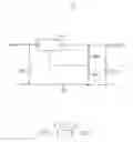
FIG. 2 shows a conventional voltage regulating circuit 10. The voltage regulating circuit 10 includes a regulator 12 with a voltage input pin 3, a voltage output pin 2, and an adjusting pin 1, two resistors RF1 and RF2, and two capacitors C10 and C20. The resistor RF1 is coupled between the voltage output pin 2 and the adjusting pin 1 of the regulator 12. The resistor RF2 is coupled between the adjusting pin 1 of the regulator 12 and ground. The capacitor C10 is coupled between the voltage input pin 3 and ground. The capacitor C20 is coupled between the voltage output pin 2 and ground.
The voltage input pin 3 is coupled to a voltage input port VIN. The voltage output pin 2 is coupled to a voltage output port VOUT. The output voltage of the output port VOUT is found using the following equation: VOUT=VREF*(1+RF2/RF1), wherein VREF is a voltage at the resistor RF1. Generally, the resistance of the resistor RF1 is 125 Ohm, and the VREF is about 1.25V. The output voltage can be varied by according to the resistance of the resistor RF2 selected. Therefore, to adjust the output voltage of the voltage regulating circuit 10, the resistor RF2 must be replaced by an operator. It is inconvenient and inefficient in voltage stability testing of a chipset to use the voltage regulating circuit 10.
What is needed, therefore, is an alterable DC power supply circuit for adjusting output voltage effectively and conveniently.
SUMMARY OF THE INVENTIONAn exemplary alterable DC power supply circuit includes a regulator, a resistor, and an adjustable load resistance. The regulator includes a voltage input pin, a voltage output pin, and an adjusting pin. The resistor is coupled between the voltage output pin and the adjusting pin. The adjustable load resistance is coupled between the adjusting pin and ground. The output voltage of the alterable DC power supply is adjustable by adjusting the adjustable load resistance.
Other advantages and novel features will become more apparent from the following detailed description when taken in conjunction with the accompanying drawings, in which:
BRIEF DESCRIPTION OF THE DRAWINGSFIG. 1 is a circuit diagram of one embodiment of an alterable DC power supply circuit in accordance with the present invention; and
FIG. 2 is a circuit diagram of a conventional voltage regulating circuit.
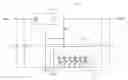
DETAILED DESCRIPTION OF THE INVENTIONReferring to FIG. 1, an alterable DC power supply circuit 20 in accordance with the present invention includes a regulator 22, a resistor R1, an adjustable load resistance 24, and five capacitors C1˜C5.
The regulator 22 includes a voltage input pin III, a voltage output pin II, and an adjusting pin I. The voltage input pin III is coupled to a voltage input port VIN. The voltage output pin II is coupled to a voltage output port VOUT. The resistor R1 is coupled between the voltage output pin II and the adjusting pin I of the regulator 22. The adjustable load resistance 24 is coupled between the adjusting pin I and ground.
The capacitor C1 is coupled between the adjusting pin I and ground for regulating a voltage at the adjustable load resistance 24. The capacitors C2 and C3 are coupled between the voltage input pin 3 and ground in parallel for regulating a voltage input from the voltage input port VIN. The capacitors C4 and C5 are coupled between the voltage output pin 2 and ground in parallel for regulating a voltage output from the output pin II of the regulator 22.
In this embodiment, the resistance of the resistor R1 is 125 Ohm, and a voltage at the resistor R1 is 1.25V. Therefore, the output voltage of the output port VOUT is found using the following equation: VOUT=1.25*(1+RL/125). Wherein RL is the resistance of the adjustable load resistance 24. The output voltage is selectable by adjusting the resistance of the adjustable load resistance 24.
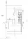
The adjustable load resistance 24 could be a sliding rheostat, a resistance box, or other adjustable resistor. In this embodiment of the present invention, the adjustable load resistance 24 includes a switch 242 and seven resistors R1˜R7 of different pre-selected values, coupled between the switch and ground in parallel. The switch 242 includes a terminal connected to the adjusting pin, and another terminal selectively connected to one of the resistors R1˜R7, and other ends of the resistors R1˜R7 are connected to ground. Therefore, the output voltage is adjustable by controlling the switch 242 to select a suitable resistance RL from the resistors R1˜R7 without having to replace a resistor. It is convenient and efficient in voltage stability testing of a chipset to use the alterable DC power supply circuit 20.
The foregoing description of the exemplary embodiments of the invention has been presented only for the purposes of illustration and description and is not intended to be exhaustive or to limit the invention to the precise forms disclosed. Many modifications and variations are possible in light of the above teaching. The embodiments were chosen and described in order to explain the principles of the invention and their practical application so as to enable others skilled in the art to utilize the invention and various embodiments and with various modifications as are suited to the particular use contemplated. Alternative embodiments will become apparent to those skilled in the art to which the present invention pertains without departing from its spirit and scope. Accordingly, the scope of the present invention is defined by the appended claims rather than the foregoing description and the exemplary embodiments described therein.
Claims
What is claimed is:1. An alterable DC power supply circuit comprising:
a regulator with a voltage input pin, a voltage output pin, and an adjusting pin;
a resistor coupled between the voltage output pin and the adjusting pin; and
an adjustable load resistance coupled between the adjusting pin and ground for adjusting an output voltage output by the regulator.
2. The alterable DC power supply circuit as claimed in claim 1, wherein the adjustable load resistance is a sliding rheostat.
3. The alterable DC power supply circuit as claimed in claim 1, wherein the adjustable load resistance is a resistance box.
4. The alterable DC power supply circuit as claimed in claim 1, wherein the adjustable load resistance comprises:
a plurality of resistors arranged in parallel, each of the resistors having a terminal connected to ground, and another terminal; and
a switch configured for selectively coupling anther terminals of the resistors to the adjusting pin of the regulator.
5. The alterable DC power supply circuit as claimed in claim 1, wherein a capacitor is coupled between the adjusting pin of the regulator and ground for regulating voltage at the adjustable load resistance.
6. The alterable DC power supply circuit as claimed in claim 1, wherein at least one capacitor is coupled between the voltage input pin of the regulator and ground.
7. The alterable DC power supply circuit as claimed in claim 1, wherein at least one capacitor is coupled between the voltage output pin of the regulator and ground.
Images & Drawings included:
Sources:
- United States Patent and Trademark Office - verify current appl. status at the USPTO↗
Recent applications in this class:
- » 20250104742 2025-03-27
Adjustable Clock and Power Gating Control - » 20250006230 2025-01-02
NEURAL NETWORK CIRCUIT AND NEURAL NETWORK CIRCUIT CONTROL METHOD - » 20240404566 2024-12-05
HEADER LAYOUT DESIGN INCLUDING BACKSIDE POWER RAIL - » 20240233780 2024-07-11
STORAGE DEVICE FOR IDLE POWER OPERATION AND METHOD THEREFOR - » 20240203461 2024-06-20
HEADER CIRCUIT PLACEMENT IN MEMORY DEVICE - » 20240055029 2024-02-15
CELL STRUCTURES AND POWER ROUTING FOR INTEGRATED CIRCUITS - » 20240029764 2024-01-25
STORAGE DEVICES FOR POWER OPTIMIZATION, STORAGE SYSTEMS INCLUDING THE SAME, AND OPERATING METHODS THEREOF - » 20230410851 2023-12-21
Header layout design including backside power rail - » 20230128141 2023-04-27
Header circuit placement in memory device - » 20220328077 2022-10-13
Header layout design including backside power rail
Recent applications for this Assignee:
- » 20120147579 2012-06-14
Printed circuit board - » 20120146915 2012-06-14
NOTEBOOK COMPUTER - » 20120146343 2012-06-14
BUTTON POSITION RECTIFYING MECHANISM - » 20120145274 2012-06-14
AIR DUCT DEVICE FOR HEAT DISSIPATION - » 20110316725 2011-12-29
SCANNING CIRCUIT AND METHOD FOR KEYBOARD - » 20110294365 2011-12-01
ELASTIC ELECTRICAL CONTACT - » 20110285558 2011-11-24
Method for storing node information of Huffman tree and corresponding decoding method - » 20110232035 2011-09-29
Hinge mechanism - » 20110227465 2011-09-22
Mounting apparatus for data storage device - » 20110188245 2011-08-04
Color LED lamp having light diffusing member and hollow isolation member with concentric optical channels