VERTICAL TRANSISTOR WITH FIELD REGION STRUCTURE
US20070117328A1
2007-05-24
11/622,429
2007-01-11
Abstract:
A structure of a vertical transistor with field region is provided. The vertical transistor comprises a field-doping region formed in a substrate next to a core region of the vertical transistor By modulating the doping density, length, and geometrical pattern of the field region, and by connecting the field region to respective well of rim core regions of the vertical transistor, the present invention realizes a stable breakdown voltage with short length of the field region. Therefore, the device area and the manufacturing cost can be reduced.
Inventors:
- TA-YUNG YANG 244 🇺🇸 MILPITAS, CA, United States
- Chih-Feng Huang 24 🇹🇼 Jhubei City, Taiwan
- Jenn-Yu G. Lin 25 🇹🇼 Taipei, Taiwan
- Tuo-Hsin Chien 10 🇹🇼 Tucheng City, Taiwan
Interested in similar patents?
Get notified when new applications in this technology area are published.
Classification:
H01L29/1095 » CPC further
Semiconductor devices adapted for rectifying, amplifying, oscillating or switching, or capacitors or resistors with at least one potential-jump barrier or surface barrier, e.g. PN junction depletion layer or carrier concentration layer; Details of semiconductor bodies or of electrodes thereof; Multistep manufacturing processes therefor; Semiconductor bodies ; Multistep manufacturing processes therefor characterised by their shape; characterised by the shapes, relative sizes, or dispositions of the semiconductor regions ; characterised by the concentration or distribution of impurities within semiconductor regions with semiconductor regions connected to an electrode not carrying current to be rectified, amplified or switched and such electrode being part of a semiconductor device which comprises three or more electrodes Body region, i.e. base region, of DMOS transistors or IGBTs
H01L29/0696 » CPC further
Semiconductor devices adapted for rectifying, amplifying, oscillating or switching, or capacitors or resistors with at least one potential-jump barrier or surface barrier, e.g. PN junction depletion layer or carrier concentration layer; Details of semiconductor bodies or of electrodes thereof; Multistep manufacturing processes therefor; Semiconductor bodies ; Multistep manufacturing processes therefor characterised by their shape; characterised by the shapes, relative sizes, or dispositions of the semiconductor regions ; characterised by the concentration or distribution of impurities within semiconductor regions characterised by the shape, relative sizes or dispositions of the semiconductor regions or junctions between the regions; Surface layout of cellular field-effect devices, e.g. multicellular DMOS transistors or IGBTs
H01L29/94 IPC
Semiconductor devices adapted for rectifying, amplifying, oscillating or switching, or capacitors or resistors with at least one potential-jump barrier or surface barrier, e.g. PN junction depletion layer or carrier concentration layer; Details of semiconductor bodies or of electrodes thereof; Multistep manufacturing processes therefor; Types of semiconductor device ; Multistep manufacturing processes therefor controllable only by variation of the electric current supplied, or only the electric potential applied, to one or more of the electrodes carrying the current to be rectified, amplified, oscillated or switched; Capacitors with potential-jump barrier or surface barrier Metal-insulator-semiconductors, e.g. MOS
Description
BACKGROUND OF THE INVENTION1. Field of the Invention
The present invention relates to semiconductor devices, and more particularly, to a vertical transistor with field region.
2. Description of Related Art
Widely applied on vertical transistor manufacturing, a field region with floating ring structure can provide a breakdown voltage. A depletion region is formed between the field region and an epi layer to increase the breakdown voltage of the vertical transistor. In order to achieve a higher breakdown voltage, the length of the field region with floating ring structure is generally long, and thus a larger device area is required. This increases the manufacturing cost. Meanwhile, due to the floating ring structure of the field region, the electric field distribution is not uniform, which renders the breakdown voltage thereof unstable.
Therefore, an improved structure for vertical transistors is desired.
SUMMARY OF THE INVENTIONOne object of the present invention is to provide an improved structure for a vertical transistor.
According to the present invention, an improved structure comprises a field region surrounding the vertical transistor. The vertical transistor is composed of an array of core regions. The field region of the present invention is connected to respective well of the rim core regions of the vertical transistor, to provide a desired breakdown voltage with a shorter length, compared with the field region in floating ring structure.
Another object of the present invention is to provide an improved structure with uniform electric field distribution for vertical transistors.
According to the present invention, the field region connected to the respective well of the rim core regions is conducted to a voltage, i.e. source voltage. The doping density of the field region is adjustable. By two means thereof, it is able to uniform the electric field distribution across the field region and the epi layer, and thus provide a stable breakdown voltage.
BRIEF DESCRIPTION OF THE DRAWINGSThese and other objects, features and advantages of the present invention will become apparent to those skilled in the art upon consideration of the following description of the embodiments of the present invention taken in conjunction with the accompanying drawings.
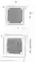
FIG. 1A shows a top view of a traditional structure of a vertical transistor.
FIG. 1B shows a top view of an improved structure of the vertical transistor according to one embodiment of the present invention.
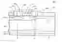
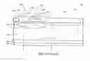
FIG. 2 shows a cross-sectional view of the traditional structure of the vertical transistor.
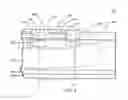
FIG. 3 shows a cross-sectional view of the improved structure of the vertical transistor according to one embodiment of the present invention.
DESCRIPTION OF THE PREFERRED EMBODIMENTSThe present invention provides an improved structure capable of ensuring a stable breakdown voltage and a desired breakdown voltage with shorter length of a field region, compared with the field region with floating ring structure.
FIG. 1A shows a top view of a traditional structure of a vertical transistor 50. A field region 106 is applied to determine a breakdown voltage range of the vertical transistor 50.
FIG. 1B illustrates a top view of an improved structure of a vertical transistor 100 according to one embodiment of the present invention. The structure of the vertical transistor 100 comprises core regions 102, a gate pad 104 connected to respective gate of each core region 102, and a field region 106a. The field region 106a formed surrounding the core regions 102 is capable of increasing the breakdown voltage of the vertical transistor 100 by the depletion region formed between the field region 106a and an epi layer 206.
FIG. 2 shows the cross-sectional view of the traditional structure of the vertical transistor 50. Each core region 102 comprises a drain metal 202, a substrate 204, the epi layer 206, a well 208, a gate oxide 210, a gate layer 212, a first heavy doping region 214, a covered shell 216, a second heavy doping region 218, and a source metal 220.
FIG. 3 shows the cross-sectional view of the improved structure of the vertical transistor 100 according to one embodiment of the present invention. The field oxide 224 is formed on the field region 106a. Unlike traditional structure of the vertical transistor 50, the field region 106a of the present invention is connected to a well 208, to thereby be conducted to a voltage, i.e. source voltage. By the applied voltage and adjustment of the doping density, the depletion region is fully depleted, and the across voltage is uniform, therefore a stable breakdown voltage can be provided. Meanwhile, the length of the field region 106a is shorter than the field region 106 in traditional structure of the vertical transistor 50, therefore the device area is reduced.
The present invention realizes a stable breakdown voltage and reduced device area by modulating the doping density, length, and geometrical pattern. of the field region 106a, and by connecting the field region 106a to the well 208.
Claims
1-2. (canceled)
3. A method for manufacturing a transistor, said method comprising steps of:
forming a field-doping region in a substrate;
forming a field oxide on said field-doping region;
forming a gate oxide on said substrate;
forming a gate layer on said gate oxide;
forming a well in said substrate;
forming a first heavy doping region in said well;
forming a covered shell over said gate oxide and said gate layer;
forming a second heavy doping region in said well next to said first heavy doping region;
forming a metal on said substrate as a electrode;
forming a backside metal on backside of said substrate as another electrode;
4. The method of claim 3, wherein the doping density of said field-doping region can be modulated for adjusting breakdown voltage.
5. The method of claim 3, wherein the length of said field-doping region can be modulated for adjusting breakdown voltage.
6. The method of claim 3, wherein the geometrical pattern of said field-doping region can be modulated for adjusting breakdown voltage.
Images & Drawings included:
Sources:
- United States Patent and Trademark Office - verify current appl. status at the USPTO↗
Similar patent applications:
- » 20060197153
Vertical transistor with field region structure - » 20210242025
SILICIDATION OF SOURCE/DRAIN REGION OF VERTICAL FIELD EFFECT TRANSISTOR (VFET) STRUCTURE - » 20150221767
Semiconductor structures with pair(s) of vertical field effect transistors, each pair having a shared source/drain region and methods of forming the structures - » 20150243765
Semiconductor structures with pair(s) of vertical field effect transistors, each pair having a shared source/drain region and methods of forming the structures - » 20060125025
Vertical field effect transistor using linear structure as a channel region and method for fabricating the same - » 20210391444
Vertical transport field-effect transistor structure having increased effective width and self-aligned anchor for source/drain region formation
Recent applications in this class:
- » 20250022950 2025-01-16
SEMICONDUCTOR DEVICE AND METHOD FOR MANUFACTURING THE SAME - » 20250006834 2025-01-02
SEMICONDUCTOR DEVICE AND FABRICATION METHOD THEREOF - » 20240395926 2024-11-28
SEMICONDUCTOR DEVICE AND METHOD FOR FABRICATING A SEMICONDUCTOR DEVICE - » 20240332414 2024-10-03
SILICON CARBIDE SEMICONDUCTOR DEVICE AND METHOD FOR PRODUCING SILICON CARBIDE SEMICONDUCTOR DEVICE - » 20240313109 2024-09-19
SEMICONDUCTOR DEVICE - » 20240313108 2024-09-19
SEMICONDUCTOR DEVICE - » 20240297249 2024-09-05
ELECTRONIC DEVICE WITH AUTO ALIGNED CSL AND EDGE TERMINATION STRUCTURE, AND MANUFACTURING METHOD THEREOF - » 20240297248 2024-09-05
SILICON CARBIDE SEMICONDUCTOR DEVICE AND METHOD FOR PRODUCING SAME - » 20240297247 2024-09-05
SILICON CARBIDE SEMICONDUCTOR DEVICE AND METHOD FOR PRODUCING SAME - » 20240290878 2024-08-29
VERTICAL POWER SEMICONDUCTOR DEVICE