Method for direct bonding of metallic conductors to a ceramic substrate
US20080156848A1
2008-07-03
11/869,749
2007-10-10
✅ Patent granted
US 7,598,164 B2
2009-10-06
-
-
Cuong Q Nguyen
2028-01-23
Abstract:
A method to provide direct bonding of wires to silicon for microelectronic and micro-electromechanical systems (MEMS). The method includes preparing a rough “pothole” during one of the many deep etch steps already provided in MEMS fabrication. The method also includes roughening of the smooth silicon surface in and around the rough pothole and plastically deforming a ball-bond into the rough pothole, such that the interconnection will eliminate a costly metallization layer, and thereby lower fabrication expenses and allow high temperature processing.
Assignee:
- TECHNION-RESEARCH &DEVELOPMENT FOUNDATION LTD. 334 🇮🇱 Haifa, Israel
Interested in similar patents?
Get notified when new applications in this technology area are published.
Classification:
B23K20/004 » CPC main
Non-electric welding by applying impact or other pressure, with or without the application of heat, e.g. cladding or plating specially adapted for particular articles or work Wire welding
H01L24/48 » CPC further
Arrangements for connecting or disconnecting semiconductor or solid-state bodies; Methods or apparatus related thereto; Means for bonding being attached to, or being formed on, the surface to be connected, e.g. chip-to-package, die-attach, "first-level" interconnects; Manufacturing methods related thereto; Wire connectors; Manufacturing methods related thereto; Structure, shape, material or disposition of the wire connectors after the connecting process of an individual wire connector
H01L24/85 » CPC further
Arrangements for connecting or disconnecting semiconductor or solid-state bodies; Methods or apparatus related thereto; Methods for connecting semiconductor or other solid state bodies using means for bonding being attached to, or being formed on, the surface to be connected using a wire connector
H01L24/45 » CPC further
Arrangements for connecting or disconnecting semiconductor or solid-state bodies; Methods or apparatus related thereto; Means for bonding being attached to, or being formed on, the surface to be connected, e.g. chip-to-package, die-attach, "first-level" interconnects; Manufacturing methods related thereto; Wire connectors; Manufacturing methods related thereto; Structure, shape, material or disposition of the wire connectors prior to the connecting process of an individual wire connector
H01L2224/4807 » CPC further
Indexing scheme for arrangements for connecting or disconnecting semiconductor or solid-state bodies and methods related thereto as covered by; Means for bonding being attached to, or being formed on, the surface to be connected, e.g. chip-to-package, die-attach, "first-level" interconnects; Manufacturing methods related thereto; Wire connectors; Manufacturing methods related thereto; Structure, shape, material or disposition of the wire connectors after the connecting process of an individual wire connector; Shape of bonding interfaces, e.g. interlocking features
H01L2224/85 » CPC further
Indexing scheme for arrangements for connecting or disconnecting semiconductor or solid-state bodies and methods related thereto as covered by; Methods for connecting semiconductor or other solid state bodies using means for bonding being attached to, or being formed on, the surface to be connected using a wire connector
H01L2924/01006 » CPC further
Indexing scheme for arrangements or methods for connecting or disconnecting semiconductor or solid-state bodies as covered by; Chemical elements Carbon [C]
H01L2924/01013 » CPC further
Indexing scheme for arrangements or methods for connecting or disconnecting semiconductor or solid-state bodies as covered by; Chemical elements Aluminum [Al]
H01L2924/01014 » CPC further
Indexing scheme for arrangements or methods for connecting or disconnecting semiconductor or solid-state bodies as covered by; Chemical elements Silicon [Si]
H01L2924/01033 » CPC further
Indexing scheme for arrangements or methods for connecting or disconnecting semiconductor or solid-state bodies as covered by; Chemical elements Arsenic [As]
H01L2924/01079 » CPC further
Indexing scheme for arrangements or methods for connecting or disconnecting semiconductor or solid-state bodies as covered by; Chemical elements Gold [Au]
H01L2224/48463 » CPC further
Indexing scheme for arrangements for connecting or disconnecting semiconductor or solid-state bodies and methods related thereto as covered by; Means for bonding being attached to, or being formed on, the surface to be connected, e.g. chip-to-package, die-attach, "first-level" interconnects; Manufacturing methods related thereto; Wire connectors; Manufacturing methods related thereto; Structure, shape, material or disposition of the wire connectors after the connecting process of an individual wire connector; Connecting portions the connecting portion on the bonding area of the semiconductor or solid-state body being a ball bond
H01L2224/78 » CPC further
Indexing scheme for arrangements for connecting or disconnecting semiconductor or solid-state bodies and methods related thereto as covered by; Apparatus for manufacturing arrangements for connecting or disconnecting semiconductor or solid-state bodies and for methods related thereto Apparatus for connecting with wire connectors
H01L2924/10253 » CPC further
Indexing scheme for arrangements or methods for connecting or disconnecting semiconductor or solid-state bodies as covered by; Details of semiconductor or other solid state devices to be connected; Material of the semiconductor or solid state bodies; Semiconducting materials; Elemental semiconductors, i.e. Group IV Silicon [Si]
H01L2924/1461 » CPC further
Indexing scheme for arrangements or methods for connecting or disconnecting semiconductor or solid-state bodies as covered by; Details of semiconductor or other solid state devices to be connected; Mixed devices MEMS
H01L2924/15787 » CPC further
Indexing scheme for arrangements or methods for connecting or disconnecting semiconductor or solid-state bodies as covered by; Details of package parts other than the semiconductor or other solid state devices to be connected; Die mounting substrate; Material with a principal constituent of the material being a non metallic, non metalloid inorganic material Ceramics, e.g. crystalline carbides, nitrides or oxides
H01L2924/00014 » CPC further
Indexing scheme for arrangements or methods for connecting or disconnecting semiconductor or solid-state bodies as covered by; Technical content checked by a classifier the subject-matter covered by the group, the symbol of which is combined with the symbol of this group, being disclosed without further technical details
H01L2224/85205 » CPC further
Indexing scheme for arrangements for connecting or disconnecting semiconductor or solid-state bodies and methods related thereto as covered by; Methods for connecting semiconductor or other solid state bodies using means for bonding being attached to, or being formed on, the surface to be connected using a wire connector; Applying energy for connecting; Compression bonding Ultrasonic bonding
H01L2924/00 » CPC further
Indexing scheme for arrangements or methods for connecting or disconnecting semiconductor or solid-state bodies as covered by
B23K31/02 IPC
Processes relevant to this subclass, specially adapted for particular articles or purposes, but not covered by only one of the preceding main groups relating to soldering or welding
H01L21/44 IPC
Processes or apparatus adapted for the manufacture or treatment of semiconductor or solid state devices or of parts thereof; Manufacture or treatment of semiconductor devices or of parts thereof the devices having at least one potential-jump barrier or surface barrier, e.g. PN junction, depletion layer or carrier concentration layer the devices having semiconductor bodies not provided for in groups, , , and with or without impurities, e.g. doping materials Manufacture of electrodes on semiconductor bodies using processes or apparatus not provided for in groups -
Description
FIELD OF THE INVENTION
The present invention relates generally to methods for bonding conductors, and more particularly to a method for direct bonding of metallic conductors to a ceramic substrate in microelectronic and MicroElectroMechanical Systems (MEMS) applications.
BACKGROUND OF THE INVENTION
Wire bonding is a method of making interconnections between a micro device and the outside world as part of semiconductor device fabrication. Wire bonding is used to electrically connect a microchip to its substrate or package. This procedure requires a metal pad on the microchip. Wire bonding is generally considered the most cost-effective and flexible interconnect technology, and is used to assemble the vast majority of semiconductor packages. In general, a gold wire is attached at both ends to a metallic layer, using some combination of heat, pressure, and ultrasonic energy to make a weld. Prior art FIG. 1a is a schematic illustration of wire bonding showing wire 105 having a standard ball-bond 110 bonded to a metal pad 120 mounted on a Single Crystal Silicon (SCS) wafer 130.
MicroElectroMechanical Systems (MEMS) and micro devices are often fabricated using passivation layers. Passivation is the process of oxidation/nitridization of a material. The passivation layers are mostly used as hard masks and electric isolation. The process of passivation requires a high temperature, of up to 1200° C.
Due to the presence of metal layers which are used as conductors and bonding pads, the process temperature is limited to 400° C. This prevents any passivation processes where metal layers exist. In micro devices the conductors may be replaced by highly doped silicon, but there is no alternative for the bonding pads, because wire bonding cannot be performed on straight smooth silicon layers.
Thus, it would be desirable to provide an alternative method that does not require bonding pads, and is not performed on straight smooth silicon layers.
SUMMARY OF THE INVENTION
Accordingly, it is a principal object of the present invention to provide direct bonding of wires to silicon.
It is another principal object of the present invention to provide roughening of the smooth silicon surface.
It is a further principal object of the present invention to take advantage of the many deep etch steps that are already included in microtechnology fabrication, wherein one of these steps is preferably used to prepare rough “potholes” into which a ball-bond can be plastically deformed.
The success of such types of interconnection will eliminate the costly metallization layer, and may lower fabrication expenses. The method of the present invention can eliminate the costly metal evaporation process, e.g. gold physical vapor deposition (Au PVD). The method also enables further processing at high temperatures, which is normally precluded by the presence of the prior art gold, or other, metal layer.
A method is disclosed for providing direct bonding of wires to silicon for microelectronics and microelectromechanical systems (MEMS). The method includes preparing a rough “pothole” during one of the many deep etch steps already provided in MEMS fabrication. The method also includes roughening of the smooth silicon surface in and around the rough pothole and plastically deforming a ball-bond into the rough pothole, such that the interconnection will obviate a costly metallization layer, and thereby lower fabrication expenses.
There has thus been outlined, rather broadly, the more important features of the invention in order that the detailed description thereof that follows hereinafter may be better understood. Additional details and advantages of the invention will be set forth in the detailed description, and in part will be appreciated from the description, or may be learned by practice of the invention.
BRIEF DESCRIPTION OF THE DRAWINGS
For a better understanding of the invention with regard to the embodiments thereof, reference is now made to the accompanying drawings, in which like numerals designate corresponding elements or sections throughout, and in which:
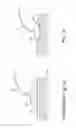
FIG. 1a is a prior art schematic illustration of a wire bonding technique showing a standard ball-bond bonded to a metal pad;
FIG. 1b is a schematic illustration of a direct bond, constructed according to the principles of the present invention; and
FIG. 2 is a schematic illustration superimposed on a microphotograph of a test structure with a wire bond directly attached to a silicon Deep Reactive Ion Etching (DRIE) pothole, according to the principles of the present invention.
DETAILED DESCRIPTION OF A PREFERRED EMBODIMENT
The principles and operation of a method and an apparatus according to the present invention may be better understood with reference to the drawings and the accompanying description, it being understood that these drawings are given for illustrative purposes only and are not meant to be limiting.
FIG. 1b is a schematic illustration of a direct bond, constructed according to the principles of the present invention. As with prior art FIG. 1a, a wire 105 is shown connected by a ball-bond 110 on a single crystal silicon (SCS) wafer 130. However, the metallic layer of FIG. 1a is replaced with a shaped pothole 140 in the microchip material. Ball-bond 110 is then pressed and deforms into pothole 140 creating a mechanical and electrical connection.
Pothole 140 can be fabricated in any geometrical shape and size. Pothole 140 will preferably include a through hole as well.
Use of a pothole to improve the electrical-mechanical interconnection is presented by way of example only.
FIG. 2 is a schematic illustration superimposed on a microphotograph of a test structure with a wire bond directly attached to a silicon Deep Reactive Ion Etching (DRIE) pothole. There are two identical test structures built in a silicon-on-insulator (SOI) wafer. In the top test structure 201, a wire bond 215 is shown electrically connecting two isolated silicon “islands” 221 and 222. In the bottom test structure 202, the two isolated silicon islands 223 and 224 are not connected, in order to give an unimpeded view of the DRIE pothole 220. The pairs of metal pads 211-212 and 213-214 are used for measuring the electrical conductivity of the direct bond.
Having described the present invention with regard to certain specific embodiments thereof, it is to be understood that the description is not meant as a limitation, since further modifications will now suggest themselves to those skilled in the art, and it is intended to cover such modifications as fall within the scope of the appended claims.
Claims
We claim:1. A method for providing direct bonding of wires to silicon for microelectronics and microelectromechanical systems (MEMS), said method comprising:
preparing a rough pothole during one of the many deep etch steps already performed in microelectronics and MEMS fabrication;
roughening of the smooth silicon surface in and around said rough pothole; and
plastically deforming a ball-bond into said rough pothole, such that the interconnection will eliminate a costly metallization layer, and thereby lower fabrication expenses and enable further high temperature processing.
2. The method according to claim 1, wherein the metallization layer eliminated is a gold layer.
3. The method according to claim 1, wherein the metallization layer eliminated is an aluminum layer.
4. The method according to claim 1, wherein the method is part of semiconductor device fabrication.
5. The method according to claim 4, wherein said fabrication uses passivation layers.
6. The method according to claim 5, wherein the passivation layers are used as hard masks.
7. The method according to claim 5, wherein the passivation layers are used as electric isolation.
8. The method according to claim 1, wherein said pothole is a silicon Deep Reactive ion Etching (DRIE) pothole.
9. A system for providing direct bonding of wires to silicon for microelectronics and microelectromechanical systems (MEMS), said system comprising:
means for preparing a rough pothole during one of the many deep etch steps already performed in microelectronics and MEMS fabrication;
means for roughening of the smooth silicon surface in and around said rough pothole; and
means for plastically deforming a ball-bond into said rough pothole, such that the interconnection will eliminate a costly metallization layer, and thereby lower fabrication expenses and enable further high temperature processing.
10. The system according to claim 9, wherein the metallization layer eliminated is a gold layer.
11. The method according to claim 1, wherein the metallization layer eliminated is an aluminum layer.
12. The system according to claim 9, wherein the system is part of semiconductor device fabrication.
13. The system according to claim 12, wherein said fabrication uses passivation layers.
14. The system according to claim 13, wherein the passivation layers are used as hard masks.
15. The system according to claim 13, wherein the passivation layers are used as electric isolation.
16. The system according to claim 9, wherein said pothole is a silicon Deep Reactive Ion Etching (DRIE) pothole.
Images & Drawings included:


Sources:
- United States Patent and Trademark Office - verify current appl. status at the USPTO↗
Recent applications in this class:
- » 20250162060 2025-05-22
WIRE BONDING SYSTEMS, WIRE REPLACEMENT SYSTEMS, AND RELATED METHODS - » 20240269764 2024-08-15
RIBBON WIRE BOND - » 20230123439 2023-04-20
WIRE GUIDE MODULE, AND ULTRASONIC WIRE BONDER THEREWITH - » 20210268598 2021-09-02
Ribbon wire bond - » 20200061735 2020-02-27
Magnet wire bonding method and bonding structure - » 20190291204 2019-09-26
RIBBON WIRE BOND - » 20180243856 2018-08-30
Ribbon bonding tools, and methods of designing ribbon bonding tools - » 20180229329 2018-08-16
BONDING APPARATUS - » 20180036832 2018-02-08
VIBRATION WELDING SYSTEM AND METHOD - » 20170282286 2017-10-05
Metal wiring bonding structure and production method therefor
Recent applications for this Assignee:
- » 20250079018 2025-03-06
METHOD DEVICE AND SYSTEM FOR MONITORING SUB-CLINCAL PROGRESSION AND REGRESSION OF HEART FAILURE - » 20240083920 2024-03-14
LOW MOLECULAR WEIGHT CORROLE COMPOSITIONS - » 20230333215 2023-10-19
DEVICE AND METHOD FOR GENERATING IMAGE AND DISTANCE INFORMATION - » 20230277258 2023-09-07
Gripper for robotic image guided needle insertion - » 20230270795 2023-08-31
GUT MICROBIOTA AND TREATMENT OF CANCER - » 20210378765 2021-12-09
Miniature bone-mounted robot for IN-SITU three-dimensional bioprinting - » 20210158545 2021-05-27
Camera-based enhancement of vehicle kinematic state estimation - » 20210109077 2021-04-15
Swab composition for detection of molecules/explosives on a surface - » 20210010463 2021-01-14
Ignition process for narrow channel hall thruster - » 20200403067 2020-12-24
Transition-metal oxides-coated hydrogen-terminated diamond surface and uses thereof