DUAL WORK FUNCTION HIGH VOLTAGE DEVICES
US20090090983A1
2009-04-09
11/866,594
2007-10-03
Abstract:
A transistor has a substrate having a channel region and source and drain regions within the substrate on opposite sides of the channel region. The structure includes a gate oxide above the channel region of the substrate and a gate conductor above the gate oxide. The polysilicon gate conductor comprises a source side positioned toward the source and a drain side positioned toward the drain. The source side comprises a first concentration of conductive doping and the drain side comprises a second concentration of the conductive doping that is less than the first concentration.
Inventors:
- Edward J. NOWAK 454 🇺🇸 Essex Junction, VT, United States
- Jeffrey P. Gambino 352 🇺🇸 Westford, VT, United States
- James W. Adkisson 135 🇺🇸 Jericho, VT, United States
- Steven H. VOLDMAN 118 🇺🇸 South Burlington, VT, United States
- Michael J. Zierak 17 🇺🇸 Essex Junction, VT, United States
Interested in similar patents?
Get notified when new applications in this technology area are published.
Classification:
H01L29/4983 » CPC main
Semiconductor devices adapted for rectifying, amplifying, oscillating or switching, or capacitors or resistors with at least one potential-jump barrier or surface barrier, e.g. PN junction depletion layer or carrier concentration layer; Details of semiconductor bodies or of electrodes thereof; Multistep manufacturing processes therefor; Electrodes ; Multistep manufacturing processes therefor characterised by the materials of which they are formed; Metal-insulator-semiconductor electrodes, e.g. gates of MOSFET with a lateral structure, e.g. a Polysilicon gate with a lateral doping variation or with a lateral composition variation or characterised by the sidewalls being composed of conductive, resistive or dielectric material
H01L29/41725 » CPC further
Semiconductor devices adapted for rectifying, amplifying, oscillating or switching, or capacitors or resistors with at least one potential-jump barrier or surface barrier, e.g. PN junction depletion layer or carrier concentration layer; Details of semiconductor bodies or of electrodes thereof; Multistep manufacturing processes therefor; Electrodes ; Multistep manufacturing processes therefor characterised by their shape, relative sizes or dispositions carrying the current to be rectified, amplified or switched Source or drain electrodes for field effect devices
H01L29/41775 » CPC further
Semiconductor devices adapted for rectifying, amplifying, oscillating or switching, or capacitors or resistors with at least one potential-jump barrier or surface barrier, e.g. PN junction depletion layer or carrier concentration layer; Details of semiconductor bodies or of electrodes thereof; Multistep manufacturing processes therefor; Electrodes ; Multistep manufacturing processes therefor characterised by their shape, relative sizes or dispositions carrying the current to be rectified, amplified or switched; Source or drain electrodes for field effect devices characterised by the proximity or the relative position of the source or drain electrode and the gate electrode, e.g. the source or drain electrode separated from the gate electrode by side-walls or spreading around or above the gate electrode
H01L29/456 » CPC further
Semiconductor devices adapted for rectifying, amplifying, oscillating or switching, or capacitors or resistors with at least one potential-jump barrier or surface barrier, e.g. PN junction depletion layer or carrier concentration layer; Details of semiconductor bodies or of electrodes thereof; Multistep manufacturing processes therefor; Electrodes ; Multistep manufacturing processes therefor characterised by the materials of which they are formed; Ohmic electrodes on silicon
H01L29/4933 » CPC further
Semiconductor devices adapted for rectifying, amplifying, oscillating or switching, or capacitors or resistors with at least one potential-jump barrier or surface barrier, e.g. PN junction depletion layer or carrier concentration layer; Details of semiconductor bodies or of electrodes thereof; Multistep manufacturing processes therefor; Electrodes ; Multistep manufacturing processes therefor characterised by the materials of which they are formed; Metal-insulator-semiconductor electrodes, e.g. gates of MOSFET the conductor material next to the insulator being a silicon layer, e.g. polysilicon doped with boron, phosphorus or nitrogen with a multiple layer structure, e.g. several silicon layers with different crystal structure or grain arrangement with a silicide layer contacting the silicon layer, e.g. Polycide gate
H01L29/78 IPC
Semiconductor devices adapted for rectifying, amplifying, oscillating or switching, or capacitors or resistors with at least one potential-jump barrier or surface barrier, e.g. PN junction depletion layer or carrier concentration layer; Details of semiconductor bodies or of electrodes thereof; Multistep manufacturing processes therefor; Types of semiconductor device ; Multistep manufacturing processes therefor controllable by only the electric current supplied, or only the electric potential applied, to an electrode which does not carry the current to be rectified, amplified or switched; Unipolar devices, e.g. field effect transistors; Field effect transistors with field effect produced by an insulated gate
Description
BACKGROUND AND SUMMARY
The embodiments of the invention generally relate to field effect transistors and more particularly to high voltage field effect transistors that utilize very thin gate oxides and a dual sided gate conductor that accommodates such devices.
High voltage field effect transistors (HV FETs) sometimes use gate dielectrics which are to thin to reliably support the high voltages experienced by such devices. These high voltages need to be reduced in some way.
The invention disclosed herein uses an intrinsic or lightly doped gate polysilicon over the drain side of the device to increase poly depletion and thereby lower the field across the gate dielectric. The drain voltage (Vdrain) allowable on a long channel FET is limited by the gate-to-drain breakdown voltage (VBD). This gate-to-drain breakdown voltage is limited by the abilities of the gate dielectric. By increasing the gate polysilicon depletion, the embodiments herein allow the gate-to-drain breakdown voltage to increase. More specifically, during conduction, the lightly doped polysilicon gate helps accumulate carriers and lower the specific on resistance (Rspon) in the region under the lightly doped polysilicon. In the “off” state, the polysilicon will deplete and drop some voltage, allowing a higher gate-to-drain voltage (Vgd) than if the gate polysilicon were fully doped.
In one structural embodiment, the invention comprises a transistor that has a substrate having a channel region (e.g., P-well) and source and drain regions within the substrate on opposite sides of the channel region. The structure includes a gate oxide above the channel region of the substrate and a gate conductor (e.g., polysilicon) above the gate oxide.
One of the features of the inventive structure is that the polysilicon gate conductor comprises a source side positioned toward the source and a drain side positioned toward the drain. The source side comprises a first concentration of conductive doping (e.g., N-type) and the drain side comprises a second concentration of the conductive doping that is less than the first concentration. More specifically, the drain side of the gate conductor has at least some of the doping, but not as much as is used in the source side. Thus, the doping in the drain side is greater than zero, but less than the first concentration amount that is in the source side of the gate conductor.
The source side and the drain side of the polysilicon gate conductor each comprise approximately one-half of the length of the gate conductor that runs between the source and the drain. Also, the conductive doping can comprise the same or different material in the source side and the drain side of the polysilicon gate conductor. Further, the concentrations that are within the source side and drain side of the gate conductor are consistent throughout each of the respective sides.
These and other aspects of the embodiments of the invention will be better appreciated and understood when considered in conjunction with the following description and the accompanying drawings. It should be understood, however, that the following descriptions, while indicating embodiments of the invention and numerous specific details thereof, are given by way of illustration and not of limitation. Many changes and modifications may be made within the scope of the embodiments of the invention without departing from the spirit thereof, and the embodiments of the invention include all such modifications.
BRIEF DESCRIPTION OF THE DRAWINGS
The embodiments of the invention will be better understood from the following detailed description with reference to the drawings, in which:
FIG. 1 is a schematic cross-sectional diagram of a transistor;
FIG. 2 is a schematic cross-sectional diagram of a transistor; and
FIG. 3 is a schematic cross-sectional diagram of a transistor.
DETAILED DESCRIPTION OF EMBODIMENTS
The embodiments of the invention and the various features and advantageous details thereof are explained more fully with reference to the non-limiting embodiments that are illustrated in the accompanying drawings and detailed in the following description. It should be noted that the features illustrated in the drawings are not necessarily drawn to scale. Descriptions of well-known components and processing techniques are omitted so as to not unnecessarily obscure the embodiments of the invention. The examples used herein are intended merely to facilitate an understanding of ways in which the embodiments of the invention may be practiced and to further enable those of skill in the art to practice the embodiments of the invention. Accordingly, the examples should not be construed as limiting the scope of the embodiments of the invention.
As mentioned above, high voltage field effect transistors (HV FETs) sometimes use gate dielectrics which are to thin to reliably support the high voltages experienced by such devices. In order to address these issues, the invention disclosed herein uses an intrinsic or lightly doped gate polysilicon over the drain side of the device to increase polysilicon depletion and thereby lower the field across the gate dielectric.
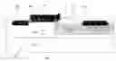
One field effect transistor, shown in FIG. 1, has a substrate 100 with a channel region 102 (e.g., P-well). Source 104 and drain 106 regions are within the substrate 100 on opposite sides of the channel region 102. The structure includes a gate oxide 108 above the channel region of the substrate and a gate conductor 110 (e.g., polysilicon) above the gate oxide. The source 104, drain 106, and gate 110 can be silicided to reduce resistance of each of these conductors.
The structure shown in FIG. 1 uses a local oxidation of silicon (LOCOS) process to create a LOCOS oxide region 112 between the gate conductor 110 and the drain 106. The oxide region 112 overlies a drift region 114. The drift region 114 reduces voltages that exist between the channel 102 and the gate conductor 110 by allowing charges to flow from the gate conductor 110 to the drain 106. Therefore, the drift region lowers voltages in the gate conductor 110 to a safe value across the dielectric 108. This drift region 114 can be an extended lightly doped drain (LDD) region which is unsilicided, or a deep implant that is below the field oxide or the shallow trench isolation region (STI).
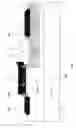
The structure shown in FIG. 2 is similar to that shown in FIG. 1, except that the transistor in FIG. 2 utilizes an unsilicided drain extension 200. Again, the excess charges can be dissipated from the gate conductor 110 to the drain 106 through the drain extension 200. However, such a structure produces a high specific on resistance (Rspon). The high on resistance of such a structure stems from the fact that doping in the extension 200 must be kept low to maintain the breakdown voltage at a high enough level. If the conductivity of the drain extension 200 were increased excessively, the breakdown voltage would fall to unacceptable levels.
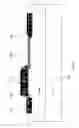
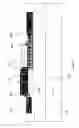
The structure shown in FIG. 3 achieves the same benefits of the structure shown in FIG. 2, without the high specific on resistance seen in the structure of FIG. 2. One of the features of the structure shown in FIG. 3 is that the polysilicon gate conductor comprises a source side 300 positioned toward the source 104 and a drain side 302 positioned toward the drain 106 and over the drain extension 200.
The source side 300 comprises a first concentration of conductive doping (e.g., high concentration N-type doping (N+)) and the drain side 302 comprises a second concentration of the conductive doping that is less than the first concentration (e.g., relatively low concentration P-type or relatively low concentration N-type doping (N− or P−)). More specifically, the drain side 302 of the gate conductor has at least some of the doping, but not as much as is used in the source side 300. Thus, the doping in the drain side 302 is greater than zero, but less than the first concentration amount that is in the source side 300 of the gate conductor. The lightly doped drain side of the gate conductor 302 depletes when the gate is off and the drain bias is high. This depleted region will support some of the gate to drain bias allowing for higher drain bias before dielectric breakdown occurs. Further, the low concentration doped drain side of the gate conductor 302 helps lower the specific on resistance (Rspon) when the gate conductor 300/302 is turned “On.”
The source side 300 and the drain side 302 of the gate conductor each comprise approximately one-half of the length of the gate conductor that runs between the source and the drain. Also, the conductive doping can comprise the same or different material in the source side 300 and the drain side 302 of the polysilicon gate conductor. Further, the concentrations that are within the source side 300 and drain side 302 of the gate conductor are consistent throughout each of the respective sides 300/302.
The drain voltage (Vdrain) allowable on a long channel FET is limited by the gate-to-drain breakdown voltage (VBD). This gate-to-drain breakdown voltage is controlled by the abilities of the gate dielectric. By increasing the gate polysilicon 300/302 depletion, the embodiments herein allow the gate-to-drain breakdown voltage to increase. More specifically, during conduction, the lightly doped polysilicon gate 302 helps accumulate carriers and lower the specific on resistance (Rspon) in the region under the lightly doped polysilicon. In the “off” state the drain side of the gate conductor 302 will deplete and drop some voltage, allowing a higher gate-to-drain voltage (Vgd) than if the gate were fully doped across its entire length.
The foregoing description of the specific embodiments will so fully reveal the general nature of the invention that others can, by applying current knowledge, readily modify and/or adapt for various applications such specific embodiments without departing from the generic concept, and, therefore, such adaptations and modifications should and are intended to be comprehended within the meaning and range of equivalents of the disclosed embodiments. It is to be understood that the phraseology or terminology employed herein is for the purpose of description and not of limitation. Therefore, while the embodiments of the invention have been described in terms of embodiments, those skilled in the art will recognize that the embodiments of the invention can be practiced with modification within the spirit and scope of the appended claims.
Claims
What is claimed is:1. A transistor comprising:
a substrate having a channel region;
source and drain regions within said substrate on opposite sides of said channel region;
a gate oxide above said channel region of said substrate;
a gate conductor above said gate oxide,
wherein said gate conductor comprises a source side positioned toward said source and a drain side positioned toward said drain,
wherein said source side comprises a first concentration of conductive doping, and
wherein said drain side comprises a second concentration of said conductive doping that is greater than zero and less than said first concentration.
2. The method according to claim 1, all the limitations of which are incorporated by reference, wherein said source side and said drain side of said gate conductor each comprise approximately one-half of a length of said gate conductor that runs between said source and said drain.
3. The method according to claim 1, all the limitations of which are incorporated by reference, wherein said conductive doping comprises a same material in said source side and said drain side of said gate conductor.
4. A transistor comprising:
a substrate having a p-well channel region;
source and drain regions within said substrate on opposite sides of said channel region;
a gate oxide above said channel region of said substrate;
a polysilicon gate conductor above said gate oxide,
wherein said polysilicon gate conductor comprises a source side positioned toward said source and a drain side positioned toward said drain,
wherein said source side comprises a first concentration of N-type conductive doping, and
wherein said drain side comprises a second concentration of said N-type conductive doping that is greater than zero and less than said first concentration.
5. The method according to claim 4, all the limitations of which are incorporated by reference, wherein said source side and said drain side of said polysilicon gate conductor each comprise approximately one-half of a length of said gate conductor that runs between said source and said drain.
6. The method according to claim 4, all the limitations of which are incorporated by reference, wherein said N-type conductive doping comprises a same material in said source side and said drain side of said polysilicon gate conductor.
Images & Drawings included:
Sources:
- United States Patent and Trademark Office - verify current appl. status at the USPTO↗
Recent applications in this class:
- » 20250040230 2025-01-30
SEMICONDUCTOR DEVICE AND MANUFACTURING METHOD OF SEMICONDUCTOR DEVICE - » 20250022936 2025-01-16
SELF-ALIGNED GATE ENDCAP (SAGE) ARCHITECTURES WITH REDUCED CAP - » 20240387681 2024-11-21
SEMICONDUCTOR DEVICES AND METHODS OF MANUFACTURE - » 20240387680 2024-11-21
FIELD-EFFECT TRANSISTOR AND METHOD OF FORMING THE SAME - » 20240363721 2024-10-31
CAPPING STRUCTURES IN SEMICONDUCTOR DEVICES - » 20240363720 2024-10-31
SEMICONDUCTOR DEVICE WITH LOW CONCENTRATION OPPOSITE TYPE DOPING DRAIN END GATE ELECTRODE - » 20240355898 2024-10-24
FIELD EFFECT TRANSISTOR WITH SPACERS AND MANUFACTURING METHOD THEREOF - » 20240258399 2024-08-01
INTEGRATED CIRCUIT DEVICE - » 20240128347 2024-04-18
SEMICONDUCTOR DEVICE - » 20240120405 2024-04-11
SEMICONDUCTOR DEVICE