Fabrication methods for integration CMOS and BJT devices
US20100041233A1
2010-02-18
12/323,404
2008-11-25
✅ Patent granted
US 8,008,212 B2
2011-08-30
-
-
Lan Vinh
2030-02-19
Abstract:
Fabrication methods for integrating CMOS and BJT devices are presented. A semiconductor substrate having a first region and a second region are provided, wherein the first region includes a CMOS device, and the second region includes a BJT device. A dielectric layer is conformably deposited on the semiconductor substrate. Part of the dielectric layer is removed, thereby forming sidewall spacers on a gate structure of the CMOS device and remaining a thin dielectric layer on the BJT device. The remaining thin dielectric layer is completely removed, completing integration of the CMOS device and the BJT device.
Inventors:
- Chien-Hsien SONG 12 🇹🇼 Kaohsiung City, Taiwan
- Yung-Lung Chou 1 🇹🇼 Ksinchu City, Taiwan
- Yu-Hsun Chen 1 🇹🇼 Changhua County, Taiwan
- Cheng-Che Tsai 1 🇹🇼 Hsinchu City, Taiwan
- Chien-Hsien Song 13 🇹🇼 Kaohsiung, Taiwan
- Yung-Lung Chou 4 🇹🇼 Hsinchu, Taiwan
- Cheng-Che Tsai 1 🇹🇼 Hsinchu, Taiwan
Assignee:
- VANGUARD INTERNATIONAL SEMICONDUCTOR CORPORATION 515 🇹🇼 HSINCHU, Taiwan
Interested in similar patents?
Get notified when new applications in this technology area are published.
Classification:
H01L21/302 IPC
Processes or apparatus adapted for the manufacture or treatment of semiconductor or solid state devices or of parts thereof; Manufacture or treatment of semiconductor devices or of parts thereof the devices having at least one potential-jump barrier or surface barrier, e.g. PN junction, depletion layer or carrier concentration layer the devices having semiconductor bodies comprising elements of Group IV of the Periodic System or AB compounds with or without impurities, e.g. doping materials; Treatment of semiconductor bodies using processes or apparatus not provided for in groups - to change their surface-physical characteristics or shape, e.g. etching, polishing, cutting
H01L27/0623 » CPC further
Devices consisting of a plurality of semiconductor or other solid-state components formed in or on a common substrate including semiconductor components specially adapted for rectifying, oscillating, amplifying or switching and having at least one potential-jump barrier or surface barrier; including integrated passive circuit elements with at least one potential-jump barrier or surface barrier the substrate being a semiconductor body including a plurality of individual components in a non-repetitive configuration integrated circuits having a two-dimensional layout of components without a common active region comprising components of the field-effect type in combination with bipolar transistors
H01L29/66272 » CPC further
Semiconductor devices adapted for rectifying, amplifying, oscillating or switching, or capacitors or resistors with at least one potential-jump barrier or surface barrier, e.g. PN junction depletion layer or carrier concentration layer; Details of semiconductor bodies or of electrodes thereof; Multistep manufacturing processes therefor; Types of semiconductor device ; Multistep manufacturing processes therefor; Multistep manufacturing processes of devices having semiconductor bodies comprising group 14 or group 13/15 materials the devices being controllable only by the electric current supplied or the electric potential applied, to an electrode which does not carry the current to be rectified, amplified or switched, e.g. three-terminal devices; Bipolar junction transistors [BJT] Silicon vertical transistors
Description
BACKGROUND OF THE INVENTION
CROSS REFERENCE TO RELATED APPLICATIONS
This application is based upon and claims the benefit of priority from a prior Taiwanese Patent Application No. 097130647, filed on Aug. 12, 2008, the entire contents of which are incorporated herein by reference.
1. Field of the Invention
The invention relates to semiconductor devices and fabrication methods thereof and in particular, to fabrication methods for integrating a CMOS and BJT device.
2. Description of the Related Art
One conventional fabrication method for integrating circuits includes integrating a complimentary metal oxide semiconductor (CMOS) transistor and (bipolar junction transistor) BJT device. Note that the characteristics of both the CMOS and BJT device have to be considered when designed in a single chip, and must not interfere with each other. For example, during a conventional etching process for the gate spacer of the CMOS device, surfaces of the BJT device may be damaged due to etching power or over etching, thereby resulting in incremental current leakage.
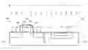
FIG. 1 is a cross section schematically illustrating conventional integration of a CMOS and BJT device. Referring to FIG. 1, a semiconductor substrate 1 is divided into two regions I and II. In region I, a CMOS transistor device 10 is formed on the semiconductor substrate 1. In region II, a BJT device 20 is formed on the semiconductor substrate. The CMOS transistor device includes a gate dielectric 13, a polysilicon gate 14 and a tungsten silicide gate 15 on the semiconductor substrate 1. Source and drain doped regions 11 and 12 are formed by the semiconductor substrate 1. The source and drain doped regions 11 and 12 of the CMOS device 10 and p-type well doped region 22, N-type doped region 24, and p-type heavy doped region 26 are formed by the same ion-implanting and diffusion processes.
Subsequently, spacers 16 are formed on both the sidewalls of the gate structure of the CMOS device 10. For example, an oxide layer is etched by a reactive ion etching process E, and spacers 16 on the sidewalls of the gate structure are formed. However, the reactive ion etching process is performed by bombardment of high power reactive ions. Thus, in order to prevent silicon oxide residue on the semiconductor substrate, over etching occurs, resulting in defects or surface damage 30 on the BJT device 20, causing incremental current leakage.
BRIEF SUMMARY OF THE INVENTION
Accordingly, in order to overcome the above-mentioned drawbacks of the background art, the processing characteristics of a CMOS and BJT device have to be considered when integrating CMOS and BJT devices. Therefore, embodiments of the invention provide fabrication methods for integrating CMOS and BJT devices to prevent current leakage in the BJT device and to improve production yields.
One embodiment of the invention provides a fabrication method for integrating CMOS and BJT devices, comprising: providing a semiconductor substrate having a first region and a second region, wherein the first region comprises a CMOS device, and wherein the second region comprises a BJT device. Additionally, a dielectric layer on the semiconductor substrate is conformably deposited and a portion of the dielectric layer is removed, thereby creating sidewall spacers on a gate structure of the CMOS device and leaving a thin dielectric layer on the BJT device. Lastly, the remaining thin dielectric layer is removed, thus completing integration of the CMOS and the BJT device.
BRIEF DESCRIPTION OF THE DRAWINGS
The invention can be more fully understood by reading the subsequent detailed description and examples with references made to the accompanying drawings, wherein:
FIG. 1 is a cross section schematically illustrating conventional integration of a CMOS and BJT device;
FIGS. 2A-2B are cross sections illustrating each step of an embodiment of a fabrication method for integrating the CMOS and BJT device; and
FIGS. 3A-3D are schematic diagrams illustrating curved relationships between operating voltage and current of the BJT device.
DETAILED DESCRIPTION OF THE INVENTION
It is to be understood that the following disclosure provides many different embodiments, or examples, for implementing different features of various embodiments. Specific examples of components and arrangements are described below to simplify the present disclosure. These are merely examples and are not intended to be limiting. In addition, the present disclosure may repeat reference numerals and/or letters in the various examples. This repetition is for the purpose of simplicity and clarity and does not in itself indicate a relationship between the various embodiments and/or configurations discussed. Moreover, the formation method for a first feature over or on a second feature in the description that follows may include embodiments in which the first and second features are formed in direct contact or not in direct contact.
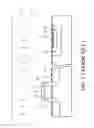
FIGS. 2A-2B are cross sections illustrating each step of an embodiment of a fabrication method for integrating of the CMOS and BJT device.
Referring to FIG. 2A, a semiconductor substrate 101 is provided. The semiconductor substrate 101 can include a single crystalline silicon substrate, a silicon-on-sapphire (SOS) substrate, or a silicon-on-insulator (SOI) substrate. The semiconductor substrate 101 can be divided into two regions I and II. In region I, a CMOS transistor device 100 is formed on the semiconductor substrate 1. In region II, a BJT device 200 is formed on the semiconductor substrate. The CMOS transistor device includes a gate dielectric 130, a polysilicon gate 140 and a metal silicide (e.g., tungsten silicide WSi) gate 150 on the semiconductor substrate 101. Source and drain (S/D) doped regions 110 and 120 are formed in the semiconductor substrate 101. The source and drain (S/D) doped regions 110 and 120 of the CMOS device 100 and p-type well doped region 220, N-type doped region 240, and p-type heavy doped region 260 of the BJT device 200 are formed by the same ion-implanting and diffusion processes.
Subsequently, a dielectric layer (such as a silicon oxide layer) is conformably formed on the semiconductor substrate 101 covering the CMOS and BJT devices. A low-power reactive ion etching E′, which is relatively 70% lower in power than conventional etching, is performed, or the etching rate is controlled such that spacers 160 are formed on both the sidewalls of the gate structure of the CMOS device 100, leaving an ultra-thin dielectric (silicon oxide) layer 165.
Referring to FIG. 2B, the remaining ultra-thin dielectric (silicon oxide) layer 165 is then removed by wet etching or by plasma ashing. Since both the wet etching and plasma ashing processes are relatively less corrosive than the conventional reactive ion etching process, surface of the BJT device 200 is not damaged during the reactive ion etching process, thereby preventing current leakage in the BJT device.
Note that in one embodiment of the invention the CMOS device of the first region comprises a logic operation device and the BJT device of the second region comprises a high voltage power supply device.
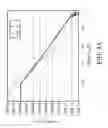
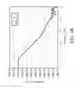
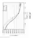
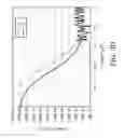
FIGS. 3A-3D are schematic diagrams illustrating curved relationships between operating voltage and current of the BJT device. As shown in FIGS. 3A-3D, surface damage on the BJT device can be prevented by reducing biasing (power) of the reactive ion etching process or reducing over-etching time during formation of the gate spacers, thereby hindering initial base leakage current (IB) problems. Moreover, when comparing FIGS. 3A-3D, its is shown that the initial base leakage current (IB) problems have been effectively addressed by reducing 30% bias (power) of the reactive ion etching process without over-etching, as shown in FIG. 3D.
While the invention has been described by way of example and in terms of the preferred embodiments, it is to be understood that the invention is not limited to the disclosed embodiments. To the contrary, it is intended to cover various modifications and similar arrangements (as would be apparent to those skilled in the art). Therefore, the scope of the appended claims should be accorded the broadest interpretation so as to encompass all such modifications and similar arrangements.
Claims
What is claimed is:1. A fabrication method for integrating CMOS and BJT devices, comprising:
providing a semiconductor substrate having a first region and a second region, wherein the first region comprises a CMOS device, and wherein the second region comprises a BJT device;
conformably depositing a dielectric layer on the semiconductor substrate;
removing a portion of the dielectric layer, thereby creating sidewall spacers on a gate structure of the CMOS device and leaving a thin dielectric layer on the BJT device; and
completely removing the remaining thin dielectric layer such that integration of the CMOS device and the BJT device is completed.
2. The fabrication method as claimed in claim 1, wherein the gate structure of the CMOS device comprises a metal silicide gate structure.
3. The fabrication method as claimed in claim 2, wherein removal of the portion of the dielectric layer comprises removing part of the dielectric layer by a reactive ion etching process.
4. The fabrication method as claimed in claim 1, wherein the process of the reactive ion etching comprises a low-power reactive ion etching.
5. The fabrication method as claimed in claim 1, wherein the step of completely removing the remaining thin dielectric layer comprises removing the remaining thin dielectric layer by wet etching.
6. The fabrication method as claimed in claim 1, wherein the CMOS device of the first region comprises a logic operation device, and wherein the BJT device of the second region comprises a high voltage power supply device.
Images & Drawings included:
Sources:
- United States Patent and Trademark Office - verify current appl. status at the USPTO↗
Recent applications in this class:
- » 20250293043 2025-09-18
METHOD OF MANUFACTURING SEMICONDUCTOR DEVICE - » 20250293042 2025-09-18
HARC ETCH CHEMISTRY FOR SEMINCONDUCTORS - » 20250293041 2025-09-18
CYCLIC ETCH/DEPOSITION PLASMA PROCESSES USING TUNGSTEN BASED PRECURSOR GAS - » 20250285875 2025-09-11
SUBSTRATE PROCESSING METHOD AND SUBSTRATE PROCESSING APPARATUS - » 20250279283 2025-09-04
SELECTIVE ETCHING OF ALTERNATING LAYERS OF SILICON OXIDE AND SILICON NITRIDE FOR HIGH ASPECT RATIO CONTACTS - » 20250279282 2025-09-04
IN SITU REMOVABLE BLOCKING LAYER FORMATION - » 20250273475 2025-08-28
QUASI-ATOMIC LAYER ETCHING OF SILICON NITRIDE ENHANCED BY REDUCED WAFER TEMPERATURE - » 20250273474 2025-08-28
METHOD AND SYSTEM FOR PROCESSING SUBSTRATE - » 20250259854 2025-08-14
PATTERN FORMATION METHOD AND METHOD OF MANUFACTURING ARTICLE - » 20250253156 2025-08-07
DEPOSITION AND ETCHING FOR SELECTIVE REMOVAL OF DEPOSITED DIELECTRIC FILM FROM TOPS OF FINS
Recent applications for this Assignee:
- » 20250294797 2025-09-18
SEMICONDUCTOR DEVICE AND METHODS FOR FORMING THE SAME - » 20250293513 2025-09-18
TRIGGER CIRCUIT AND OPERATING CIRCUIT - » 20250287687 2025-09-11
SEMICONDUCTOR DEVICE AND METHODS FOR FORMING THE SAME - » 20250260403 2025-08-14
LEVEL SHIFTER - » 20250241000 2025-07-24
HIGH-VOLTAGE SEMICONDUCTOR DEVICE - » 20250230038 2025-07-17
MICRO-ELECTRO-MECHANICAL SYSTEM PACKAGE AND FABRICATION METHOD THEREOF - » 20250230037 2025-07-17
MICRO-ELECTRO-MECHANICAL SYSTEM PACKAGE AND FABRICATION METHOD THEREOF - » 20250212448 2025-06-26
ELECTROSTATIC DISCHARGE PROTECTION DEVICE - » 20250194139 2025-06-12
SEMICONDUCTOR DEVICE - » 20250189723 2025-06-12
SEMICONDUCTOR DEVICE AND FABRICATION METHOD THEREOF