Less expensive high power plastic surface mount package
US20100109147A1
2010-05-06
12/590,377
2009-11-06
✅ Patent granted
US 8,274,164 B2
2012-09-25
-
-
Marcos D. Pizarro | Eva Yan Montalvo
2029-11-06
Abstract:
A high power surface mount package including a thick bond line of solder interposed between the die and a heatsink, and between the die and a lead frame, wherein the lead frame has the same coefficient of thermal expansion as the heatsink. In one preferred embodiment, the heatsink and the lead frame are comprised of the same material. The package can be assembled using standard automated equipment, and does not require a weight or clip to force the parts close together, which force typically reduces the solder bond line thickness. Advantageously, the thermal stresses on each side of the die are effectively balanced, allowing for a large surface area die to be packaged with conventional and less expensive materials. One type of die that benefits from the present invention can include a transient voltage suppressor, but could include other dies generating a significant amount of heat, such as those in excess of 0.200 inches square.
Assignee:
- MICROSEMI CORPORATION 79 🇺🇸 Irvine, CA, United States
Interested in similar patents?
Get notified when new applications in this technology area are published.
Classification:
H01L2224/92 » CPC further
Indexing scheme for arrangements for connecting or disconnecting semiconductor or solid-state bodies and methods related thereto as covered by; Methods for connecting semiconductor or solid state bodies including different methods provided for in two or more of groups - Specific sequence of method steps
H01L2224/83 » CPC further
Indexing scheme for arrangements for connecting or disconnecting semiconductor or solid-state bodies and methods related thereto as covered by; Methods for connecting semiconductor or other solid state bodies using means for bonding being attached to, or being formed on, the surface to be connected using a layer connector
H01L2224/84 » CPC further
Indexing scheme for arrangements for connecting or disconnecting semiconductor or solid-state bodies and methods related thereto as covered by; Methods for connecting semiconductor or other solid state bodies using means for bonding being attached to, or being formed on, the surface to be connected using a strap connector
H01L2924/014 » CPC further
Indexing scheme for arrangements or methods for connecting or disconnecting semiconductor or solid-state bodies as covered by; Alloys Solder alloys
H01L2924/0132 » CPC further
Indexing scheme for arrangements or methods for connecting or disconnecting semiconductor or solid-state bodies as covered by; Alloys Binary Alloys
H01L2924/0105 » CPC further
Indexing scheme for arrangements or methods for connecting or disconnecting semiconductor or solid-state bodies as covered by; Chemical elements Tin [Sn]
H01L2924/3512 » CPC further
Indexing scheme for arrangements or methods for connecting or disconnecting semiconductor or solid-state bodies as covered by; Technical effects; Mechanical effects; Thermal stress Cracking
H01L2924/00014 » CPC further
Indexing scheme for arrangements or methods for connecting or disconnecting semiconductor or solid-state bodies as covered by; Technical content checked by a classifier the subject-matter covered by the group, the symbol of which is combined with the symbol of this group, being disclosed without further technical details
H01L2924/01047 » CPC further
Indexing scheme for arrangements or methods for connecting or disconnecting semiconductor or solid-state bodies as covered by; Chemical elements Silver [Ag]
H01L2924/01082 » CPC further
Indexing scheme for arrangements or methods for connecting or disconnecting semiconductor or solid-state bodies as covered by; Chemical elements Lead [Pb]
H01L24/40 » CPC main
Arrangements for connecting or disconnecting semiconductor or solid-state bodies; Methods or apparatus related thereto; Means for bonding being attached to, or being formed on, the surface to be connected, e.g. chip-to-package, die-attach, "first-level" interconnects; Manufacturing methods related thereto; Strap connectors, e.g. copper straps for grounding power devices; Manufacturing methods related thereto; Structure, shape, material or disposition of the strap connectors after the connecting process of an individual strap connector
H01L23/4334 » CPC further
Details of semiconductor or other solid state devices; Arrangements for cooling, heating, ventilating or temperature compensation ; Temperature sensing arrangements; Fillings or auxiliary members in containers or encapsulations selected or arranged to facilitate heating or cooling; Auxiliary members in containers characterised by their shape, e.g. pistons Auxiliary members in encapsulations
H01L23/49513 » CPC further
Details of semiconductor or other solid state devices; Arrangements for conducting electric current to or from the solid state body in operation, e.g. leads, terminal arrangements ; Selection of materials therefor consisting of soldered constructions; Lead-frames or other flat leads characterised by the die pad having bonding material between chip and die pad
H01L23/49562 » CPC further
Details of semiconductor or other solid state devices; Arrangements for conducting electric current to or from the solid state body in operation, e.g. leads, terminal arrangements ; Selection of materials therefor consisting of soldered constructions; Lead-frames or other flat leads; Geometry of the lead-frame for devices being provided for in
H01L24/27 » CPC further
Arrangements for connecting or disconnecting semiconductor or solid-state bodies; Methods or apparatus related thereto; Means for bonding being attached to, or being formed on, the surface to be connected, e.g. chip-to-package, die-attach, "first-level" interconnects; Manufacturing methods related thereto; Layer connectors, e.g. plate connectors, solder or adhesive layers; Manufacturing methods related thereto Manufacturing methods
H01L24/29 » CPC further
Arrangements for connecting or disconnecting semiconductor or solid-state bodies; Methods or apparatus related thereto; Means for bonding being attached to, or being formed on, the surface to be connected, e.g. chip-to-package, die-attach, "first-level" interconnects; Manufacturing methods related thereto; Layer connectors, e.g. plate connectors, solder or adhesive layers; Manufacturing methods related thereto; Structure, shape, material or disposition of the layer connectors prior to the connecting process of an individual layer connector
H01L24/33 » CPC further
Arrangements for connecting or disconnecting semiconductor or solid-state bodies; Methods or apparatus related thereto; Means for bonding being attached to, or being formed on, the surface to be connected, e.g. chip-to-package, die-attach, "first-level" interconnects; Manufacturing methods related thereto; Layer connectors, e.g. plate connectors, solder or adhesive layers; Manufacturing methods related thereto; Structure, shape, material or disposition of the layer connectors after the connecting process of a plurality of layer connectors
H01L24/37 » CPC further
Arrangements for connecting or disconnecting semiconductor or solid-state bodies; Methods or apparatus related thereto; Means for bonding being attached to, or being formed on, the surface to be connected, e.g. chip-to-package, die-attach, "first-level" interconnects; Manufacturing methods related thereto; Strap connectors, e.g. copper straps for grounding power devices; Manufacturing methods related thereto; Structure, shape, material or disposition of the strap connectors prior to the connecting process of an individual strap connector
H01L2924/10253 » CPC further
Indexing scheme for arrangements or methods for connecting or disconnecting semiconductor or solid-state bodies as covered by; Details of semiconductor or other solid state devices to be connected; Material of the semiconductor or solid state bodies; Semiconducting materials; Elemental semiconductors, i.e. Group IV Silicon [Si]
H01L24/73 » CPC further
Arrangements for connecting or disconnecting semiconductor or solid-state bodies; Methods or apparatus related thereto Means for bonding being of different types provided for in two or more of groups , , , , , , ,
H01L24/83 » CPC further
Arrangements for connecting or disconnecting semiconductor or solid-state bodies; Methods or apparatus related thereto; Methods for connecting semiconductor or other solid state bodies using means for bonding being attached to, or being formed on, the surface to be connected using a layer connector
H01L24/84 » CPC further
Arrangements for connecting or disconnecting semiconductor or solid-state bodies; Methods or apparatus related thereto; Methods for connecting semiconductor or other solid state bodies using means for bonding being attached to, or being formed on, the surface to be connected using a strap connector
H01L24/92 » CPC further
Arrangements for connecting or disconnecting semiconductor or solid-state bodies; Methods or apparatus related thereto; Methods for connecting semiconductor or solid state bodies including different methods provided for in two or more of groups - Specific sequence of method steps
H01L2224/83192 » CPC further
Indexing scheme for arrangements for connecting or disconnecting semiconductor or solid-state bodies and methods related thereto as covered by; Methods for connecting semiconductor or other solid state bodies using means for bonding being attached to, or being formed on, the surface to be connected using a layer connector; Arrangement of the layer connectors prior to mounting wherein the layer connectors are disposed only on another item or body to be connected to the semiconductor or solid-state body
H01L2224/838 » CPC further
Indexing scheme for arrangements for connecting or disconnecting semiconductor or solid-state bodies and methods related thereto as covered by; Methods for connecting semiconductor or other solid state bodies using means for bonding being attached to, or being formed on, the surface to be connected using a layer connector Bonding techniques
H01L2224/83801 » CPC further
Indexing scheme for arrangements for connecting or disconnecting semiconductor or solid-state bodies and methods related thereto as covered by; Methods for connecting semiconductor or other solid state bodies using means for bonding being attached to, or being formed on, the surface to be connected using a layer connector; Bonding techniques Soldering or alloying
H01L2224/84801 » CPC further
Indexing scheme for arrangements for connecting or disconnecting semiconductor or solid-state bodies and methods related thereto as covered by; Methods for connecting semiconductor or other solid state bodies using means for bonding being attached to, or being formed on, the surface to be connected using a strap connector; Bonding techniques Soldering or alloying
H01L2924/01029 » CPC further
Indexing scheme for arrangements or methods for connecting or disconnecting semiconductor or solid-state bodies as covered by; Chemical elements Copper [Cu]
H01L2924/01075 » CPC further
Indexing scheme for arrangements or methods for connecting or disconnecting semiconductor or solid-state bodies as covered by; Chemical elements Rhenium [Re]
H01L2924/157 » CPC further
Indexing scheme for arrangements or methods for connecting or disconnecting semiconductor or solid-state bodies as covered by; Details of package parts other than the semiconductor or other solid state devices to be connected; Die mounting substrate; Material with a principal constituent of the material being a metal or a metalloid, e.g. boron [B], silicon [Si], germanium [Ge], arsenic [As], antimony [Sb], tellurium [Te] and polonium [Po], and alloys thereof
H01L2924/351 » CPC further
Indexing scheme for arrangements or methods for connecting or disconnecting semiconductor or solid-state bodies as covered by; Technical effects; Mechanical effects Thermal stress
H01L2924/00 » CPC further
Indexing scheme for arrangements or methods for connecting or disconnecting semiconductor or solid-state bodies as covered by
H01L2924/181 » CPC further
Indexing scheme for arrangements or methods for connecting or disconnecting semiconductor or solid-state bodies as covered by; Details of package parts other than the semiconductor or other solid state devices to be connected Encapsulation
H01L2924/00012 » CPC further
Indexing scheme for arrangements or methods for connecting or disconnecting semiconductor or solid-state bodies as covered by; Technical content checked by a classifier Relevant to the scope of the group, the symbol of which is combined with the symbol of this group
H01L23/488 IPC
Details of semiconductor or other solid state devices; Arrangements for conducting electric current to or from the solid state body in operation, e.g. leads, terminal arrangements ; Selection of materials therefor consisting of soldered constructions
H01L21/60 IPC
Processes or apparatus adapted for the manufacture or treatment of semiconductor or solid state devices or of parts thereof; Manufacture or treatment of semiconductor devices or of parts thereof the devices having at least one potential-jump barrier or surface barrier, e.g. PN junction, depletion layer or carrier concentration layer; Assembly of semiconductor devices using processes or apparatus not provided for in a single one of the subgroups - , e.g. sealing of a cap to a base of a container Attaching or detaching leads or other conductive members, to be used for carrying current to or from the device in operation
H01L23/36 IPC
Details of semiconductor or other solid state devices; Arrangements for cooling, heating, ventilating or temperature compensation ; Temperature sensing arrangements Selection of materials, or shaping, to facilitate cooling or heating, e.g. heatsinks
H01L23/28 IPC
Details of semiconductor or other solid state devices Encapsulations, e.g. encapsulating layers, coatings, e.g. for protection
Description
CLAIM OF PRIORITY
This application claims priority of U.S. Provisional Ser. No. 61/198,478 filed Nov. 6, 2008, entitled “Less Expensive High Power Plastic Surface Mount Package”, the teachings of which are incorporated herein by reference.
FIELD OF THE INVENTION
The present invention is generally related to semiconductor packages, and more particularly to large area high power dies having thermal cooling.
BACKGROUND OF THE INVENTION
Semiconductor packages typically comprise an enclosed die that generates a certain amount of heat during operation. Some semiconductor dies are high power devices that generate a significant amount of heat, such as transient voltage suppressors. Cooling devices are often employed to facilitate the dissipation of thermal heat, such as heatsinks and the like. Typically, the semiconductor die is mechanically and thermally coupled to the heatsink, and may be joined thereto by a thin solder bond line.
Semiconductor die typically have a low coefficient of thermal expansion, such as silicon die. In contrast, heatsinks typically have a high thermal coefficient of thermal expansion as they typically comprise of metal materials. Thus, the materials expand at different rates as a function of temperature during operation which can crack and damage the die over varying operating temperatures. It is conventional in the industry to implement more expensive materials to thermally match and join the die to the high coefficient of thermal expansion materials. Typically, these thermal matching materials are interposed between the die and the thermal cooling member, such as the heatsink.
There is desired a less expensive high power surface mount package that eliminates the need for expensive thermal matching materials, and particularly a large surface area die having large surface areas.
SUMMARY OF INVENTION
The present invention achieves technical advantages as a high power surface mount package including a thick bond line of solder interposed between the die and a heatsink, and between the die and a lead frame, wherein the lead frame has the same coefficient of thermal expansion as the heatsink. In one preferred embodiment, the heatsink and the lead frame are comprised of the same material. The package can be assembled using standard automated equipment, and does not require a weight or clip to force the parts close together, which force typically reduces the solder bond line thickness. Advantageously, the thermal stresses on each side of the die are effectively balanced to prevent damage to the die over temperature cycles, allowing for a large surface area die to be packaged with conventional and inexpensive materials. One type of die that benefits from the present invention can include a transient voltage suppressor, but could include other dies generating a significant amount of heat, such as those in excess of 0.200 inches square.
BRIEF DESCRIPTION OF THE DRAWINGS
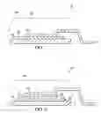
FIG. 1 is a side elevational view of a large area high power semiconductor die package according to one preferred embodiment of the present invention;
FIG. 2 is an side sectional view taken vertically thru the package of FIG. 1, illustrating the thick solder bond lines disposed between the die and the respective heatsink and lead frame; and
FIG. 3 is a flow diagram of an assembly process according to one preferred embodiment of the present invention.
DETAILED DESCRIPTION OF THE PREFERRED EMBODIMENT
Referring now to FIG. 1 there is generally shown at 10 a high power surface mount package according to one preferred embodiment of the present invention. Package 10 is seen to comprise a large surface area die 12 interposed between a large heatsink 14 and a lead frame 16 in a sandwich-like configuration.
Referring to FIG. 2 there is shown an enlarged side sectional view of the package 10 shown in FIG. 1. Advantageously, a relatively thick solder bond line 20 is disposed between the lower major surface of the large die 12 and heatsink 14. In addition, a relatively thick solder bond line 22 is formed between the top major surface of the die 12 and the lead frame 16 thereabove, as shown. According to one aspect of the present invention, the heatsink 14 and the lead frame 16 have substantially the same coefficient of thermal expansion. In another aspect of the present invention, the heatsink 12 and the lead frame 16 are comprised of the same materials, and thus have the same coefficient of thermal expansion. In one preferred embodiment both the heatsink and the lead frame are comprised of copper, although limitation to this material is not to be inferred.
The thicknesses of the solder bond lines 20 and 22 are relatively thick and thus provide additional mechanical support to the die 12 to prevent flexing. The thickness of these solder bond lines 20 and 22 are preferably at least 0.005 inches thickness, although this thickness could be greater than or less than this thickness as desired, such as 0.001 inches or even 0.010 inches or greater, depending on the designed parameters, expected temperature cycles for intended operation of the die, and the choice of materials for the heatsink 12 and lead frame 16. These solder bond lines are easily formed during manufacture by eliminating a weight or clipping force of the package during heating to melt/re-flow the solder materials. It is noted that the thickness of the solder bond lines 20 and 22 are exaggerated in FIG. 2 for purposes of illustration.
Advantageously, matching the coefficient of thermal expansion of the heatsink 14 to the lead frame 16 balances any residual mechanical stress to the large surface area die 12 due to any thermal expansion mismatch. Preferably, the thick solder bond lines 20 and 22 are comprised of very common inexpensive materials, such as a Pb/Tin solder paste. In one preferred embodiment, the solder paste may have a melting point of 280° Celsius and is re-flowed at 300° Celsius. Solder paste comprised of 88Pb10Sn2Ag has been found to be suitable, and limitation to this material is not to be inferred.
A typical die size may be 0.200 inches square or greater, and may have a surface area of 0.210 inches square in one preferred embodiment, and have a thickness of 0.012 inches. In one preferred embodiment, the semiconductor may be a diode, such as a transient voltage suppressor suitable for use in an automotive application.
Method of Manufacture
Referring to FIG. 3 in view of FIG. 2, one preferred method for packaging the present invention is shown.
At Step 30, the lead frame 16 is loaded into an alignment fixture (not shown).
At step 32, a solder paste corresponding to solder bond line 22 is dispensed onto the lead frame 16, such as a Pb/Tin solder as previously described.
At step 34, the die 12 is placed onto the solder paste of step 32.
At step 36 solder paste is dispensed onto the die 12, which may also be an inexpensive conventional Pb/Tin solder having the same or similar thickness as the solder paste dispensed in step 32. The width of the solder paste may differ from that of step 32, depending on the length/width of the die and the dimensions of the lead frame 16.
At step 38, the heatsink 14 is placed on the solder paste dispensed in step 36.
Preferably, the lead frame 16 and heatsink 14 are comprised of the same material, such as copper, as previously described.
At step 40, the stack of parts from steps 30, 32, 34, 36 and 38 are put thru a 300° Celsius oven to re-flow the solder paste and advantageously form the thick solder bond lines 20 and 22. Advantageously, the stack of parts are not provided with a weight or clip to force the piece parts closed together during solder re-flow, which would otherwise reduce the thickness of the solder bond lines 20 and 22. It is noted that other methods can be used to control the bond line thickness as desired.
At step 42 the parts are cleaned to remove residue from the solder paste created during the re-flow solder.
At step 44, the sub-assembly is over molded with a transfer mold compound, shown in phantom lines, which may comprise of plastic, but could also comprise of ceramic or other materials as desired.
At step 46, the assembly is post cured in an oven at 175° Celsius for about 1 hour to complete curing the mold compound.
Though the invention has been described with respect to a specific preferred embodiment, many variations and modifications will become apparent to those skilled in the art upon reading the present application. The intention is therefore that the appended claims be interpreted as broadly as possible in view of the prior art to include all such variations and modifications.
Claims
What is claimed is:1. A semiconductor package, comprising:
a semiconductor die having a first major surface and a second major surface;
a lead frame having a first coefficient of thermal expansion;
a first solder material having a first thickness and disposed between the semiconductor die first major surface and the lead frame;
a heatsink having a second coefficient of thermal expansion;
a second solder material having a second thickness and disposed between the semiconductor die second major surface and the heatsink;
wherein the first coefficient of thermal expansion and the second coefficient of thermal expansion are substantially the same.
2. The semiconductor package as specified in claim 1 wherein the lead and the heatsink are comprised of the same material.
3. The semiconductor package as specified in claim 1 wherein the first coefficient of thermal expansion and the second coefficient of thermal expansion are the same.
4. The semiconductor package as specified in claim 1 wherein the first solder material has a thickness of at least 0.005.
5. The semiconductor package as specified in claim 4 wherein the second solder material has a thickness of at least 0.005.
6. The semiconductor package as specified in claim 1 wherein the first and second solder materials each have a coefficient of thermal expansion that are substantially the same.
7. The semiconductor package as specified in claim 6 wherein the first and second solder materials are comprised of the same material.
8. The semiconductor package as specified in claim 6 wherein at least the first solder material or the second solder material is comprised of lead and tin.
9. The semiconductor package as specified in claim 8 wherein both the first solder material and the second solder material are comprised of 88Pb10Sn2Af solder.
10. The semiconductor package as specified in claim 1 wherein the semiconductor die comprises a transient voltage suppressor.
11. A method of forming a semiconductor package, comprising the steps of:
disposing a first solder paste having a first coefficient of thermal expansion on a lead;
disposing a semiconductor die on the first solder paste;
disposing a second solder paste on the semiconductor die;
disposing a heatsink having a second coefficient of thermal expansion on the second solder paste; and
heating the recited elements above to melt the first and second solder paste.
12. The method as specified in claim 11 wherein no force is applied to the recited elements during the heating step.
13. The method as specified in claim 10 wherein the lead and the heatsink are comprised of the same material.
14. The method as specified in claim 10 wherein the first coefficient of thermal expansion and the second coefficient of thermal expansion are the same.
15. The method as specified in claim 10 wherein the first solder material has a thickness of at least 0.005.
16. The method as specified in claim 14 wherein the second solder material has a thickness of at least 0.005.
17. The method as specified in claim 11 wherein the first and second solder materials each have a coefficient of thermal expansion that are substantially the same.
18. The method as specified in claim 16 wherein the first and second solder materials are comprised of the same material.
19. The method as specified in claim 16 wherein at least the first solder material or the second solder material is comprised of lead and tin.
20. The method as specified in claim 18 wherein both the first solder material and the second solder material are comprised of 88Pb10Sn2Af solder.
Images & Drawings included:


Sources:
- United States Patent and Trademark Office - verify current appl. status at the USPTO↗
Similar patent applications:
Recent applications in this class:
- » 20250286011 2025-09-11
SEMICONDUCTOR PACKAGE WITH HYBRID INTERCONNECT CLIP - » 20250279388 2025-09-04
SEMICONDUCTOR DEVICE - » 20250253284 2025-08-07
Multi-Die Integrated Circuit Device with a Spark Gap - » 20250246572 2025-07-31
CLIP DESIGN AND METHOD OF CONTROLLING CLIP POSITION - » 20250233099 2025-07-17
SEMICONDUCTOR DEVICE AND METHOD FOR MANUFACTURING SEMICONDUCTOR DEVICE - » 20250210579 2025-06-26
POWER STAGE DEVICE CLIP - » 20250192093 2025-06-12
SEMICONDUCTOR DEVICE AND METHODS OF MANUFACTURING SEMICONDUCTOR DEVICEs - » 20250183219 2025-06-05
SEMICONDUCTOR PACKAGES WITH CHIP STACK - » 20250132282 2025-04-24
CONTACT DEVICE AND POWER MODULE ARRANGEMENT - » 20250118699 2025-04-10
SEMICONDUCTOR DEVICE
Recent applications for this Assignee:
- » 20120032728 2012-02-09
Auto-optimization circuits and methods for cyclical electronic systems - » 20120032708 2012-02-09
Gate driver power and control signal transmission circuits and methods - » 20120032664 2012-02-09
SINGLE INDUCTOR POWER CONVERTER SYSTEM AND METHODS - » 20120009886 2012-01-12
Architecture for coexistence of multiple band radios - » 20110242767 2011-10-06
Mechanical isolation and thermal conductivity for an electro-magnetic device - » 20110181204 2011-07-28
Balancing transformers for multi-lamp operation - » 20100315167 2010-12-16
Inter-stage matching network to enhance common mode stability - » 20100277125 2010-11-04
Battery charging and discharging by using a bi-directional transistor - » 20100245001 2010-09-30
Coaxial-to-microstrip transitions - » 20100136748 2010-06-03
Flexible diode package and method of manufacturing