CHIP PACKAGE AND MANUFACTURING METHOD THEREOF
US20100110656A1
2010-05-06
12/388,771
2009-02-19
Abstract:
A chip package including a plurality of conductive bodies and a shielding layer for better electromagnetic interferences shielding is provided. The shielding layer over the molding compound contacts with the conductive bodies disposed on the substrate, and the shielding layer and the conductive bodies function as EMI shield. The shielding layer is electrically grounded through the conductive bodies connected to the laminate substrate and the ground plane of the substrate.
Inventors:
- Dongkyun Ko 3 🇰🇷 Kyunggi-Do, South Korea
- Jung Lee 3 🇰🇷 Kyunggi-Do, South Korea
- Jaesun An 3 🇰🇷 Kyunggi-Do, South Korea
Assignee:
- ADVANCED SEMICONDUCTOR ENGINEERING, INC. 1,850 🇹🇼 Kaohsiung, Taiwan
Interested in similar patents?
Get notified when new applications in this technology area are published.
Classification:
H01L21/78 » CPC main
Processes or apparatus adapted for the manufacture or treatment of semiconductor or solid state devices or of parts thereof; Manufacture or treatment of devices consisting of a plurality of solid state components formed in or on a common substrate or of parts thereof; Manufacture of integrated circuit devices or of parts thereof; Manufacture or treatment of devices consisting of a plurality of solid state components or integrated circuits formed in, or on, a common substrate with subsequent division of the substrate into plural individual devices
H01L21/561 » CPC further
Processes or apparatus adapted for the manufacture or treatment of semiconductor or solid state devices or of parts thereof; Manufacture or treatment of semiconductor devices or of parts thereof the devices having at least one potential-jump barrier or surface barrier, e.g. PN junction, depletion layer or carrier concentration layer; Assembly of semiconductor devices using processes or apparatus not provided for in a single one of the subgroups - , e.g. sealing of a cap to a base of a container; Encapsulations, e.g. encapsulation layers, coatings Batch processing
H01L23/3121 » CPC further
Details of semiconductor or other solid state devices; Encapsulations, e.g. encapsulating layers, coatings, e.g. for protection characterised by the arrangement or shape the device being completely enclosed a substrate forming part of the encapsulation
H01L23/552 » CPC further
Details of semiconductor or other solid state devices Protection against radiation, e.g. light or electromagnetic waves
H01L24/97 » CPC further
Arrangements for connecting or disconnecting semiconductor or solid-state bodies; Methods or apparatus related thereto; Batch processes at chip-level, i.e. with connecting carried out on a plurality of singulated devices, i.e. on diced chips the devices being connected to a common substrate, e.g. interposer, said common substrate being separable into individual assemblies after connecting
H05K1/0218 » CPC further
Printed circuits; Details; Electrical arrangements not otherwise provided for; Reduction of cross-talk, noise or electromagnetic interference by printed shielding conductors, ground planes or power plane
H05K1/0218 » CPC further
Printed circuits; Details; Electrical arrangements not otherwise provided for; Reduction of cross-talk, noise or electromagnetic interference by printed shielding conductors, ground planes or power plane
H01L2924/01006 » CPC further
Indexing scheme for arrangements or methods for connecting or disconnecting semiconductor or solid-state bodies as covered by; Chemical elements Carbon [C]
H01L2924/01013 » CPC further
Indexing scheme for arrangements or methods for connecting or disconnecting semiconductor or solid-state bodies as covered by; Chemical elements Aluminum [Al]
H01L2924/01024 » CPC further
Indexing scheme for arrangements or methods for connecting or disconnecting semiconductor or solid-state bodies as covered by; Chemical elements Chromium [Cr]
H01L2924/01029 » CPC further
Indexing scheme for arrangements or methods for connecting or disconnecting semiconductor or solid-state bodies as covered by; Chemical elements Copper [Cu]
H01L2924/01033 » CPC further
Indexing scheme for arrangements or methods for connecting or disconnecting semiconductor or solid-state bodies as covered by; Chemical elements Arsenic [As]
H01L2924/01047 » CPC further
Indexing scheme for arrangements or methods for connecting or disconnecting semiconductor or solid-state bodies as covered by; Chemical elements Silver [Ag]
H01L2924/01078 » CPC further
Indexing scheme for arrangements or methods for connecting or disconnecting semiconductor or solid-state bodies as covered by; Chemical elements Platinum [Pt]
H01L2924/01079 » CPC further
Indexing scheme for arrangements or methods for connecting or disconnecting semiconductor or solid-state bodies as covered by; Chemical elements Gold [Au]
H01L2924/014 » CPC further
Indexing scheme for arrangements or methods for connecting or disconnecting semiconductor or solid-state bodies as covered by; Alloys Solder alloys
H01L2924/15311 » CPC further
Indexing scheme for arrangements or methods for connecting or disconnecting semiconductor or solid-state bodies as covered by; Details of package parts other than the semiconductor or other solid state devices to be connected; Die mounting substrate; Connection portion the connection portion being formed only on the surface of the substrate opposite to the die mounting surface being a ball array, e.g. BGA
H01L2924/15313 » CPC further
Indexing scheme for arrangements or methods for connecting or disconnecting semiconductor or solid-state bodies as covered by; Details of package parts other than the semiconductor or other solid state devices to be connected; Die mounting substrate; Connection portion the connection portion being formed only on the surface of the substrate opposite to the die mounting surface being a land array, e.g. LGA
H01L2924/1815 » CPC further
Indexing scheme for arrangements or methods for connecting or disconnecting semiconductor or solid-state bodies as covered by; Details of package parts other than the semiconductor or other solid state devices to be connected; Encapsulation Shape
H01L2924/3025 » CPC further
Indexing scheme for arrangements or methods for connecting or disconnecting semiconductor or solid-state bodies as covered by; Technical effects; Electrical effects Electromagnetic shielding
H05K3/0032 » CPC further
Apparatus or processes for manufacturing printed circuits; Working of insulating substrates or insulating layers; Etching of the substrate by chemical or physical means by laser ablation of organic insulating material
H05K3/0032 » CPC further
Apparatus or processes for manufacturing printed circuits; Working of insulating substrates or insulating layers; Etching of the substrate by chemical or physical means by laser ablation of organic insulating material
H05K3/0052 » CPC further
Apparatus or processes for manufacturing printed circuits; Working of insulating substrates or insulating layers; Mechanical working of the substrate, e.g. drilling or punching Depaneling, i.e. dividing a panel into circuit boards; Working of the edges of circuit boards
H05K3/0052 » CPC further
Apparatus or processes for manufacturing printed circuits; Working of insulating substrates or insulating layers; Mechanical working of the substrate, e.g. drilling or punching Depaneling, i.e. dividing a panel into circuit boards; Working of the edges of circuit boards
H05K3/284 » CPC further
Apparatus or processes for manufacturing printed circuits; Secondary treatment of printed circuits; Applying non-metallic protective coatings for encapsulating mounted components
H05K3/284 » CPC further
Apparatus or processes for manufacturing printed circuits; Secondary treatment of printed circuits; Applying non-metallic protective coatings for encapsulating mounted components
H05K2203/0415 » CPC further
Indexing scheme relating to apparatus or processes for manufacturing printed circuits covered by; Soldering or other types of metallurgic bonding Small preforms other than balls, e.g. discs, cylinders or pillars
H05K2203/0415 » CPC further
Indexing scheme relating to apparatus or processes for manufacturing printed circuits covered by; Soldering or other types of metallurgic bonding Small preforms other than balls, e.g. discs, cylinders or pillars
H01L2224/97 » CPC further
Indexing scheme for arrangements for connecting or disconnecting semiconductor or solid-state bodies and methods related thereto as covered by; Batch processes at chip-level, i.e. with connecting carried out on a plurality of singulated devices, i.e. on diced chips the devices being connected to a common substrate, e.g. interposer, said common substrate being separable into individual assemblies after connecting
H01L2224/81 » CPC further
Indexing scheme for arrangements for connecting or disconnecting semiconductor or solid-state bodies and methods related thereto as covered by; Methods for connecting semiconductor or other solid state bodies using means for bonding being attached to, or being formed on, the surface to be connected using a bump connector
H01L2924/181 » CPC further
Indexing scheme for arrangements or methods for connecting or disconnecting semiconductor or solid-state bodies as covered by; Details of package parts other than the semiconductor or other solid state devices to be connected Encapsulation
H01L2924/14 » CPC further
Indexing scheme for arrangements or methods for connecting or disconnecting semiconductor or solid-state bodies as covered by; Details of semiconductor or other solid state devices to be connected; Device type Integrated circuits
H01L2924/00 » CPC further
Indexing scheme for arrangements or methods for connecting or disconnecting semiconductor or solid-state bodies as covered by
H01L2924/00014 » CPC further
Indexing scheme for arrangements or methods for connecting or disconnecting semiconductor or solid-state bodies as covered by; Technical content checked by a classifier the subject-matter covered by the group, the symbol of which is combined with the symbol of this group, being disclosed without further technical details
H01L2924/00011 » CPC further
Indexing scheme for arrangements or methods for connecting or disconnecting semiconductor or solid-state bodies as covered by; Technical content checked by a classifier Not relevant to the scope of the group, the symbol of which is combined with the symbol of this group
H01L2224/0401 » CPC further
Indexing scheme for arrangements for connecting or disconnecting semiconductor or solid-state bodies and methods related thereto as covered by; Means for bonding being attached to, or being formed on, the surface to be connected, e.g. chip-to-package, die-attach, "first-level" interconnects; Manufacturing methods related thereto; Bonding areas; Manufacturing methods related thereto; Structure, shape, material or disposition of the bonding areas prior to the connecting process Bonding areas specifically adapted for bump connectors, e.g. under bump metallisation [UBM]
H05K9/00 IPC
Screening of apparatus or components against electric or magnetic fields
H05K9/00 IPC
Screening of apparatus or components against electric or magnetic fields
Description
CROSS-REFERENCE TO RELATED APPLICATION
This application claims the priority benefit of U.S. provisional application Ser. No. 61/109,937, filed on Oct. 31, 2008. The entirety of the above-mentioned patent application is hereby incorporated by reference herein and made a part of specification.
BACKGROUND OF THE INVENTION
1. Field of the Invention
The present invention relates to a semiconductor device, and more particularly to a chip package.
2. Description of Related Art
Electro-magnetic interference (EMI) is a serious and challenging problem for most electronic devices or systems. As EMI disturbances commonly interrupt, degrade or limit the effective performance of the electronic device or the whole circuit of the electronic system, it is necessary for the electronic devices or systems to have efficient EMI protection to ensure the effective and safe operation.
EMI protection is particularly important in small-sized, densely packaged or sensitive electronic applications operating at high frequencies. Conventionally, EMI shielding solutions typically involve the use of metal plates and/or conductive gaskets, which are later attached or affixed at higher manufacturing costs.
SUMMARY OF THE INVENTION
In view of the foregoing, the present invention provides a manufacturing method of a chip package, which offers better design flexibility with less effort.
The present invention is further directed to a chip package with enhanced effectiveness of EMI shielding.
The present invention provides a chip package including a laminate substrate, at least a chip disposed on the laminate substrate, a plurality of conductive bodies, a molding compound and a shielding layer. The conductive bodies disposed on the laminate substrate are arranged around the chip. The molding compound at least encapsulates the chip, a portion of the laminate substrate and the conductive bodies, but partially exposes top surfaces of the conductive bodies. The shielding layer disposed over the molding compound covers not only the molding compound but also the exposed top surface of each conductive body.
According to embodiments of the present invention, either solder materials or parts of the leadframe or printed circuit board can be used to form the conductive bodies.
According to embodiments of the present invention, the conductive bodies can be arranged at the boundary lines of the laminate substrate and at least a side surface of each conductive body is exposed.
According to embodiments of the present invention, the conductive bodies can be arranged along the boundary lines of the laminate substrate and the side surfaces of each conductive body are not exposed.
According to embodiments of the present invention, the chip is electrically connected to the laminate substrate of the chip package though a plurality of bumps.
The invention further provides a manufacturing method of a chip package. A plurality of conductive bodies are formed on each substrate unit of the provided matrix substrate and arranged around the die attaching region of the substrate unit. At least a chip is disposed on the die attaching region of the substrate unit, and the chip is electrically connected to the substrate unit. After forming a molding compound over the matrix substrate to encapsulate the chip, portions of the substrate units and the conductive bodies, a marking process is performed to remove a portion of the molding compound until a top surface of each conductive body is exposed. Later, a shielding layer is formed over the molding compound to cover the molding compound and the exposed top surface of each conductive body. Then a singulation process is performed to obtain a plurality of chip packages.
According to one embodiment of the present invention, the conductive bodies can be arranged on sawing lines of the matrix substrate and on boundary lines of each substrate unit, or arranged around boundary lines of each substrate unit with a distance apart.
According to one embodiment of the present invention, the conductive bodies are formed from a metallic material by a spraying process, a sputtering process or a plating process, or formed from a solder material by a spraying process or a printing process.
According to one embodiment of the present invention, the marking process comprises a laser digging process or a laser drilling process.
Based on the above, the shielding layer and the connected conductive bodies disposed on the substrate functions as an EMI shield of the chip package for the surrounding EMI radiation. According to the present invention, a complete EMI shielding is achieved through the shielding layer and the conductive bodies with flexible and variable designs. Therefore, the chip package of the present invention has better EMI shielding effectiveness and improved process windows.
In order to the make the aforementioned and other objects, features and advantages of the present invention comprehensible, several embodiments accompanied with figures are described in detail below.
BRIEF DESCRIPTION OF THE DRAWINGS
FIGS. 1A through 1G are schematic views showing a manufacturing method of the chip package according to one preferred embodiment of the present invention.
FIG. 2 is a cross-sectional view of a chip package according to an embodiment of the present invention.
FIG. 3 is a cross-sectional view of a chip package according to another embodiment of the present invention.
DESCRIPTION OF EMBODIMENTS
Reference will now be made in detail to the present preferred embodiments of the invention, examples of which are illustrated in the accompanying drawings. Wherever possible, the same reference numbers are used in the drawings and the description to refer to the same or like parts.
The manufacturing methods as described in the present invention can be used for fabricating various package structures and are more suitable for fabricating stacked type packages, multiple-chip packages, or high frequency device packages (including radio frequency device packages). Moreover, the manufacturing methods as described in the present invention are compatible with packaging processes utilizing build-up substrate manufacturing process or array substrate manufacturing process.
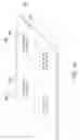
FIGS. 1A through 1G are schematic views showing a manufacturing method of the chip package according to the preferred embodiment of the present invention. FIGS. 1A, 1B, 1B′ and 1C are shown in three-dimensional schematic views, while FIGS. 1D-1G are shown in cross-sectional schematic views.
Referring to FIG. 1A, a matrix substrate 100 having a plurality of substrate 102 (defined by the subsequent sawing lines shown as dotted lines) is provided, while each substrate 102 includes a plurality of contacts 104 thereon. The contacts 104 are arranged within the die attaching area 103 of each substrate 102. The contacts 104 function as bump pads for flip chip connecting technology. The substrate 100 can be a laminate substrate, for example, a printed circuit board (PCB).
Referring to FIG. 1B, a plurality of conductive bodies 110 is disposed over the top surface 102a of the substrate 102, outside the die attaching area 103. Preferably, the conductive bodies 110 are arranged around the boundary or perimeter of each substrate 102. As shown in FIG. 1B, the individual conductive bodies 110 are arranged right on the boundary lines of the substrate 102 (the dotted lines). In this case, the subsequent sawing process will cut through the conductive bodies 110 arranged along the sawing lines.
On the other hand, the individual conductive bodies 110 may be arranged along the boundary lines of the substrate 102 but are not exactly located on the boundary lines of the substrate 102 (the dotted lines), as shown in FIG. 1B′. The conductive bodies 110 may be arranged close to the boundary lines of the substrate 102, separate by a small distance d, and d can be varied according to product requirements. However, the subsequent sawing process will not cut through the conductive bodies 110 arranged along the sawing lines.
The conductive body 110 can be made of a solder material, for example. Alternatively, the conductive body 110 can be made from a conductive carrier, such as, a leadframe or a laminate printed circuit board. The shape of the conductive body 110 can be polygonal blocks (shown as rectangular blocks in FIG. 1B or 1B′). However, the conductive body 110 can be shaped as blocks, strips or even connected with one another as a ring structure, for example. In general, the sizes or the shape of conductive body 110 can be varied depending on the shielding requisites or other electrical properties of the package or even varied in accordance with the processing parameters.
If a multi-layered substrate, such as a multi-layered PCB, is employed, it is possible to form the conductive bodies 110 from the routing manufacturing step of the build-up substrate manufacturing process. That is, during the routing process to form the traces of the substrate, the conductive bodies can be formed by the same process as patterned metallic blocks, other than the traces.
Referring to FIG. 1C, at least a chip 120 is disposed on each substrate 102 and within attaching area 103. Although a chip is provided herein, other surface mount components can be employed, and encompassed within the scope of this invention. The chip 120 is electrically connected to the contacts 104 of the substrate 102 through a plurality of bumps 106 (shown in FIG. 1D) there-between. Although flip chip connecting technology is described herein, it is well encompassed within the scope of this invention to employ wire bonding technology (i.e. through wire connections). The chip 120 should be completely separated from the conductive bodies 110.
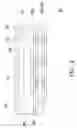
Referring to FIG. 1D, a molding process is carried out to form a molding compound 130 on the matrix substrate 100 to encapsulate the conductive bodies 110, the chips 120, the bumps 106 and at least a portion of the substrate 102. The molding process can be an over-molding process, for example. Although the conductive body 110 is depicted as higher than the total height of the chip 120 and the bumps 106, it is optional to form the conductive body 110 with a height smaller or larger than the total height of the chip 120 and the bumps 106.
Referring to FIG. 1E, a marking process is performed to remove portions of the molding compound 130 over the conductive bodies 110, so that the top surface 110a of each conductive body 110 is at least partially exposed. The top surface 110a of the conductive body can be partially exposed or completely exposed. The marking process may include a laser drilling process or a laser digging process, for example. Taking the conductive bodies arranged around the boundary of each substrate 102 as an example, the marking process may removes portions of the molding compound 130 by forming a ring-like trench within the molding compound 130 over the conductive bodies 110, around the boundary of each substrate 102.
Referring to FIG. 1F, a shielding layer 140 is formed over the molding compound 130 to cover the molding compound 130 and the exposed top surfaces 110a of the conductive bodies 110. The shielding layer 140 can be formed by a spray coating method, a plating method, or a sputtering method, for example.
Finally, referring to FIG. 1G, a singulation process is performed to obtain the individual chip packages 10. The singulation process may be a blade sawing process, for example.
FIG. 2 is a cross-sectional view of a chip package according to a preferred embodiment of the present invention. Referring to FIG. 2, the chip package 20 of the present embodiment includes a substrate 102, a plurality of bumps 106, a plurality of conductive bodies 110, at least a chip 120, a molding compound 130 and a shielding layer 140. The substrate 102 can be a laminated substrate, for example, a two-layered or a four-layered laminated PCB substrate. The chip 120 can be a semiconductor chip, for example, a radio-frequency (RF) chip. The material of the shielding layer 140 may be copper, aluminum or alloys thereof or even a solder material, for example. The chips 120 are electrically connected to the substrates 102 through bumps 106. The molding compound 130 encapsulates portions of the substrates 102, the conductive bodies 110, and the chips 120. Besides, the shielding layer 140 is disposed over the molding compound 130, covering the top surface of the molding compound 130 and the exposed top surfaces 110a of the conductive bodies 110. The shielding layer 140 is electrically connected to the substrate 102 through the conductive bodies 110.
For example, the conductive body 110 can be made from a laminated PCB or a leadframe (i.e. be a chunk or a piece of a laminated PCB or a leadframe), for example. If the conductive body 110 is a piece of a laminated PCB, the shielding layer 140 can be electrically connected to the substrate 102 through vias or plated through-holes of the conductive bodies 110, for example. If the conductive body 110 is a piece of a leadframe, the shielding layer 140 can be electrically connected to the substrate 102 through the conductive bodies 110 and the conductive bodies 110 can be fixed to the substrate 102 through conductive adhesives, such as anisotropy conductive films (ACF), for example. Alternatively, the conductive body 110 can be made of a solder material; i.e. be a solder lump, strip or a solder ring structure, for example.
In addition, the conductive body 110 is connected to a ground vias 108 of the substrate 102, and the shielding layer 140 is electrically grounded through the conductive body 110 and the ground via 108. Hence, taking advantage of the metal wirings or traces of the substrate surface, the shielding layer of the present invention can be grounded within the package structure using the ground plane of the substrate. It should be noted that at least a sidewall 110b of each conductive body 110 is aligned with the edge of the shielding layer 140, as the sawing process cuts through the conductive bodies arranged on the sawing street lines. That is, the sidewall 110b of each conductive body 110 is exposed.
According to another embodiment, as shown in FIG. 3, the sidewall 110b of each conductive body 110 is not exposed and is covered by the molding compound 130. Instead, the conductive bodies 110 are fully encapsulated by the molding compound 130, except the exposed top surface 110a. The sidewall 130b of the molding compound is aligned with an edge of the shielding layer, through the cutting of the singulation process. Basically, the package structure 30 follows the manufacturing step shown in FIG. 1B′ (rather than FIG. 1B), and the sawing process does not cut through the conductive bodies arranged around the sawing street lines.
In the chip package structures of the present embodiment, the shielding layer and the conductive bodies disposed on the substrate together function as an EMI shield, protecting the package from the EMI radiation from the surrounding radiation sources.
Furthermore, as the shielding layer is formed over the whole matrix substrate and the molding compound before the singulation process, no half-cutting process is required and the process window is increased and the reliability is improved.
In summary, the shielding layer and the conductive bodies can efficiently shelter the chip package of the present invention from the outside EMI radiation, thus boosting the EMI shielding. Following the manufacturing processes disclosed in the present invention, it is possible to establish an electrical ground path within the package structure, devoid of using an extra ground plane. Accordingly, such design is compatible with the packaging of high frequency devices, particularly, radio frequency devices.
Although the present invention has been disclosed above by the embodiments, they are not intended to limit the present invention. Anybody skilled in the art can make some modifications and alteration without departing from the spirit and scope of the present invention. Therefore, the protecting range of the present invention falls in the appended claims.
Claims
What is claimed is:1. A chip package, comprising:
a laminate substrate;
at least a chip disposed on the laminate substrate;
a plurality of conductive bodies disposed on the laminate substrate and around the chip;
a molding compound, at least encapsulating the chip, a portion of the laminate substrate and the plurality of the conductive bodies; and
a shielding layer, disposed over the molding compound, covering the molding compound and partially covering at least a top surface of each conductive body exposed by the molding compound.
2. The chip package as claimed in claim 1, wherein at least a sidewall of each conductive body is exposed and is aligned with an edge of the shielding layer.
3. The chip package as claimed in claim 1, wherein sidewalls of the conductive bodies are covered by the molding compound and an edge of the molding compound is aligned with an edge of the shielding layer.
4. The chip package as claimed in claim 1, wherein the chip is electrically connected to the contacts through a plurality of bumps arranged underneath the chip.
5. The chip package as claimed in claim 1, wherein the conductive bodies are arranged around the chip as a ring, and the chip is separated from the conductive bodies.
6. The chip package as claimed in claim 1, wherein the chip is a radio frequency chip.
7. The chip package as claimed in claim 1, wherein the shielding layer is electrically connected to the laminate substrate via the conductive body and at least a ground via of the laminate substrate.
8. The chip package as claimed in claim 1, wherein the conductive body is made of a solder material and the conductive body is a solder block.
9. The chip package as claimed in claim 1, wherein the conductive body is a part of a printed circuit board.
10. The chip package as claimed in claim 1, wherein the conductive body is a part of a leadframe.
11. The chip package as claimed in claim 1, wherein a material of the shielding layer is a metal material.
12. A manufacturing method of a chip package, comprising:
providing a matrix substrate having a plurality of substrate units, wherein each substrate unit is defined by a plurality of sawing lines and has a die attaching region thereon;
forming a plurality of conductive bodies on each substrate unit and arranged around the die attaching region;
disposing at least a chip on the die attaching region of the substrate unit, wherein the chip is electrically connected to the substrate unit, and the plurality of conductive bodies is separated from the chip;
forming a molding compound over the matrix substrate to encapsulate the chip, portions of the substrate units and the conductive bodies;
performing a marking process to remove a portion of the molding compound until a top surface of each conductive body is exposed;
forming a shielding layer over the molding compound to cover the molding compound and the exposed top surface of each conductive body; and
performing a singulation process to obtain a plurality of chip packages.
13. The method as claimed in claim 12, wherein the conductive bodies are arranged on sawing lines of the matrix substrate and on boundary lines of each substrate unit.
14. The method as claimed in claim 12, wherein the conductive bodies are arranged around boundary lines of each substrate unit with a distance apart.
15. The method as claimed in claim 12, wherein the conductive bodies are formed from a metallic material by a spraying process, a sputtering process or a plating process.
16. The method as claimed in claim 12, wherein the conductive bodies are formed from a solder material by a spraying process or a printing process.
17. The method as claimed in claim 12, wherein the marking process comprises a laser digging process or a laser drilling process.
18. The method as claimed in claim 12, wherein the chip is electrically connected to the substrate through flip chip bonding.
Images & Drawings included:


Sources:
- United States Patent and Trademark Office - verify current appl. status at the USPTO↗
Similar patent applications:
- » 20230005758
PACKAGED CHIP AND MANUFACTURING METHOD THEREOF, REWIRED PACKAGED CHIP AND MANUFACTURING METHOD THEREOF - » 20150235947
Multi chip package, manufacturing method thereof, and memory system having the multi chip package - » 20120267791
Multi chip package, manufacturing method thereof, and memory system having the multi chip package - » 20190295984
Embedded chip package, manufacturing method thereof, and package-on-package structure - » 20240178103
Chip Stacked Structure and Manufacturing Method Thereof, Chip Package Structure, and Electronic Device - » 20230361082
CHIP STACKING STRUCTURE AND MANUFACTURING METHOD THEREOF, CHIP PACKAGE STRUCTURE, AND ELECTRONIC DEVICE - » 20220102164
Vertical interconnection structure and manufacturing method thereof, packaged chip, and chip packaging method - » 20250029954
SEMICONDUCTOR DEVICES AND MANUFACTURING METHODS THEREOF, CHIP PACKAGE STRUCTURES - » 20090189296
FLIP CHIP QUAD FLAT NON-LEADED PACKAGE STRUCTURE AND MANUFACTURING METHOD THEREOF AND CHIP PACKAGE STRUCTURE - » 20140102772
Packaging carrier and manufacturing method thereof and chip package structure
Recent applications in this class:
- » 20250167049 2025-05-22
WAFER PROCESSING METHOD - » 20250157858 2025-05-15
LASER DICING FOR SINGULATION - » 20250157857 2025-05-15
COMPONENT AND METHOD OF MANUFACTURING A COMPONENT USING AN ULTRATHIN CARRIER - » 20250149386 2025-05-08
DIE CLEANING SYSTEMS AND RELATED METHODS - » 20250149385 2025-05-08
METHOD FOR MANUFACTURING SEMICONDUCTOR DEVICE - » 20250149384 2025-05-08
METHOD FOR DICING A SEMICONDUCTOR WAFER STRUCTURE - » 20250140613 2025-05-01
METHOD OF PROCESSING WAFER - » 20250140612 2025-05-01
METHOD FOR WAFER DICING - » 20250125198 2025-04-17
PROCESSING METHOD - » 20250125197 2025-04-17
SEMICONDUCTOR CHIP
Recent applications for this Assignee:
- » 20250174898 2025-05-29
ANTENNA DEVICE - » 20250174536 2025-05-29
ELECTRONIC PACKAGE STRUCTURE - » 20250174508 2025-05-29
SEMICONDUCTOR DEVICE PACKAGE - » 20250167440 2025-05-22
SEMICONDUCTOR DEVICE PACKAGE AND METHOD OF MANUFACTURING THE SAME - » 20250167131 2025-05-22
OPTICAL PACKAGE STRUCTURE - » 20250167092 2025-05-22
ELECTRONIC DEVICE - » 20250159793 2025-05-15
ELECTRONIC DEVICE - » 20250157972 2025-05-15
ELECTRONIC PACKAGE STRUCTURE AND METHOD FOR MANUFACTURING THE SAME - » 20250157947 2025-05-15
WIRING STRUCTURE AND METHOD FOR MANUFACTURING THE SAME - » 20250157888 2025-05-15
ELECTRONIC DEVICE