Ohmic Contact Having Silver Material
US20100283153A1
2010-11-11
12/651,991
2010-01-04
Abstract:
An ohmic contact is fabricated. The ohmic contact has low electric resistivity and high thermal conductivity. The materials for fabricating the ohmic contact include silver. Thus, equipments for fabricating the ohmic contact are compatible to modern generally used equipments.
Assignee:
- ATOMIC ENERGY COUNCIL- INSTITUTE OF NUCLEAR ENERGY RESEARCH 158 🇹🇼 Taoyuan, Taiwan
Interested in similar patents?
Get notified when new applications in this technology area are published.
Classification:
H01L24/02 » CPC main
Arrangements for connecting or disconnecting semiconductor or solid-state bodies; Methods or apparatus related thereto; Means for bonding being attached to, or being formed on, the surface to be connected, e.g. chip-to-package, die-attach, "first-level" interconnects; Manufacturing methods related thereto Bonding areas ; Manufacturing methods related thereto
H01L33/40 » CPC further
Semiconductor devices with at least one potential-jump barrier or surface barrier specially adapted for light emission; Processes or apparatus specially adapted for the manufacture or treatment thereof or of parts thereof; Details thereof characterised by the electrodes Materials therefor
H01L29/452 » CPC further
Semiconductor devices adapted for rectifying, amplifying, oscillating or switching, or capacitors or resistors with at least one potential-jump barrier or surface barrier, e.g. PN junction depletion layer or carrier concentration layer; Details of semiconductor bodies or of electrodes thereof; Multistep manufacturing processes therefor; Electrodes ; Multistep manufacturing processes therefor characterised by the materials of which they are formed; Ohmic electrodes on AIII-BV compounds
H01L31/022425 » CPC further
Semiconductor devices sensitive to infra-red radiation, light, electromagnetic radiation of shorter wavelength or corpuscular radiation and specially adapted either for the conversion of the energy of such radiation into electrical energy or for the control of electrical energy by such radiation; Processes or apparatus specially adapted for the manufacture or treatment thereof or of parts thereof; Details thereof; Details; Electrodes for devices characterised by at least one potential jump barrier or surface barrier for solar cells
H01L33/30 » CPC further
Semiconductor devices with at least one potential-jump barrier or surface barrier specially adapted for light emission; Processes or apparatus specially adapted for the manufacture or treatment thereof or of parts thereof; Details thereof characterised by the semiconductor bodies; Materials of the light emitting region containing only elements of group III and group V of the periodic system
H01L2224/0401 » CPC further
Indexing scheme for arrangements for connecting or disconnecting semiconductor or solid-state bodies and methods related thereto as covered by; Means for bonding being attached to, or being formed on, the surface to be connected, e.g. chip-to-package, die-attach, "first-level" interconnects; Manufacturing methods related thereto; Bonding areas; Manufacturing methods related thereto; Structure, shape, material or disposition of the bonding areas prior to the connecting process Bonding areas specifically adapted for bump connectors, e.g. under bump metallisation [UBM]
H01L2924/01006 » CPC further
Indexing scheme for arrangements or methods for connecting or disconnecting semiconductor or solid-state bodies as covered by; Chemical elements Carbon [C]
H01L2924/01023 » CPC further
Indexing scheme for arrangements or methods for connecting or disconnecting semiconductor or solid-state bodies as covered by; Chemical elements Vanadium [V]
H01L2924/01033 » CPC further
Indexing scheme for arrangements or methods for connecting or disconnecting semiconductor or solid-state bodies as covered by; Chemical elements Arsenic [As]
H01L2924/01046 » CPC further
Indexing scheme for arrangements or methods for connecting or disconnecting semiconductor or solid-state bodies as covered by; Chemical elements Palladium [Pd]
H01L2924/01047 » CPC further
Indexing scheme for arrangements or methods for connecting or disconnecting semiconductor or solid-state bodies as covered by; Chemical elements Silver [Ag]
H01L2924/01078 » CPC further
Indexing scheme for arrangements or methods for connecting or disconnecting semiconductor or solid-state bodies as covered by; Chemical elements Platinum [Pt]
H01L2924/01079 » CPC further
Indexing scheme for arrangements or methods for connecting or disconnecting semiconductor or solid-state bodies as covered by; Chemical elements Gold [Au]
H01L2924/10329 » CPC further
Indexing scheme for arrangements or methods for connecting or disconnecting semiconductor or solid-state bodies as covered by; Details of semiconductor or other solid state devices to be connected; Material of the semiconductor or solid state bodies; Semiconducting materials; Compound semiconductors; III-V Gallium arsenide [GaAs]
H01L2933/0016 » CPC further
Details relating to devices covered by the group but not provided for in its subgroups; Processes relating to electrodes
Y02E10/50 » CPC further
Energy generation through renewable energy sources Photovoltaic [PV] energy
Y02E10/50 » CPC further
Energy generation through renewable energy sources Photovoltaic [PV] energy
H01L2924/12041 » CPC further
Indexing scheme for arrangements or methods for connecting or disconnecting semiconductor or solid-state bodies as covered by; Details of semiconductor or other solid state devices to be connected; Device type; Passive devices, e.g. 2 terminal devices; Optical Diode LED
H01L2924/00 » CPC further
Indexing scheme for arrangements or methods for connecting or disconnecting semiconductor or solid-state bodies as covered by
H01L23/48 IPC
Details of semiconductor or other solid state devices Arrangements for conducting electric current to or from the solid state body in operation, e.g. leads, terminal arrangements ; Selection of materials therefor
Description
FIELD OF THE INVENTION
The present invention relates to an ohmic contact; more particularly, relates to an ohmic contact having low electric resistivity and high thermal conductivity, which contains silver and is compatible with modern arts to be fabricated with low cost.
DESCRIPTION OF THE RELATED ARTS
Almost every semiconductor device needs an ohmic contact having low resistance to optimize its performance. It is because a contact having high resistance will produce too much heat and thus weaken the device. Generally, the ohmic contact for gallium arsenide (GaAs) semiconductor is made of an alloy of AuGe/Ni and the contact is made through anneal at a temperature between 400° C. and 500° C.
But, the ohmic contact is made with gold, not silver having lower electric conductivity and higher heat conductivity. In addition, gold is more expensive than silver, which make the production cost higher. Hence, the prior art does not fulfill all users' requests on actual use.
SUMMARY OF THE INVENTION
The main purpose of the present invention is to provide an ohmic contact having low electric resistivity and high thermal conductivity, which contains silver and is compatible with modern arts to be fabricated with low cost.
To achieve the above purpose, the present invention is an ohmic contact containing silver, comprising an ohmic contact and an n-type III-V compound semiconductor layer, where the ohmic contact comprises a nickel (Ni) layer, a germanium (Ge) layer, a silver (Ag) layer, a palladium (Pd) or platinum (Pt) layer, and a thick metal layer; and; where the Ni layer, the Ge layer, the Ag layer, the Pd or Pt layer and the thick metal layer are sequentially stacked on the n-type III-V compound semiconductor layer; and where the ohmic contact is obtained by being processed through annealing. Accordingly, a novel ohmic contact containing silver is obtained.
BRIEF DESCRIPTIONS OF THE DRAWINGS
The present invention will be better understood from the following detailed description of the preferred embodiment according to the present invention, taken in conjunction with the accompanying drawings, in which
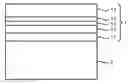
FIG. 1 is the sectional view showing the structure of the preferred embodiment according to the present invention; and
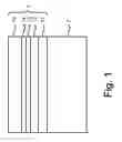
FIG. 2 is the view showing the analysis of electric resistivity and thermal conductivity.
DESCRIPTION OF THE PREFERRED EMBODIMENT
The following description of the preferred embodiment is provided to understand the features and the structures of the present invention.
Please refer to FIG. 1 and FIG. 2, which are a sectional view showing a structure of a preferred embodiment according to the present invention; and a view showing an analysis of electric resistivity and thermal conductivity. As shown in the figures, the present invention is an ohmic contact containing silver, comprising an ohmic contact 1 and a n-type III-V compound semiconductor layer 2, where the ohmic contact 1 comprises a nickel (Ni) layer 11, a germanium (Ge) layer 12, a silver (Ag) layer 13, a palladium (Pd) or platinum (Pt) layer 14, and a thick metal layer 15; and the Ni layer 11, the Ge layer 12, the Ag layer 13, the Pd or Pt layer 14 and the thick metal layer 15 are sequentially stacked on the n-type III-V compound semiconductor layer 2. Therein, the ohmic contact 1 obtains a structure body by being processed through annealing at a temperature between 300° C. and 500° C.; the Ni layer 11 has a thickness between 1 nanometer (nm) and 20 nm; the Ge layer 12 has a thickness between 1 nm and 50 nm; the Ag layer 13 has a thickness between 5 nm and 200 nm; and the Pd layer 14 has a thickness between 20 nm and 200 nm (or, the Pt layer has a thickness between 10 nm and 200 nm.) Thus, a novel ohmic contact containing silver is obtained.
At first, a Ni layer 11, a Ge layer 12, an Ag layer 13, a Pd or Pt layer 14 and a thick metal layer 15 of an ohmic contact 1 are sequentially deposed on an n-type III-V compound semiconductor layer through evaporation deposition or electroplating deposition, where the n-type III-V compound semiconductor layer 2 is a gallium arsenide (GaAs) layer.
Thus, through annealing, the ohmic contact 1 obtains low electric resistivity and high thermal conductivity. The low electric resistivity and the high thermal conductivity of the ohmic contact 1 are obtained by controlling thicknesses of the metal layers coordinated with the annealing temperature, where a thickness ratio of the Ag layer 13 to the Ge layer 12 lies between 7 and 8 and the annealing temperature is 400° C. In the other hand, the n-type III-V compound semiconductor layer 2 is made of light emitting diode (LED), laser diode, solar cell or transistor.
In the present invention, the ohmic contact contains silver, which has good electric conductivity and thermal conductivity and is compatible with modern arts. Furthermore, silver is cheaper than gold (as shown in FIG. 2) so the ohmic contact fabricated is cheaper.
To sum up, the present invention is an ohmic contact containing silver, where the ohmic contact has low electric resistivity and high thermal conductivity; and the present invention contains silver and is compatible with modern arts to be fabricated with low cost.
The preferred embodiment herein disclosed is not intended to unnecessarily limit the scope of the invention. Therefore, simple modifications or variations belonging to the equivalent of the scope of the claims and the instructions disclosed herein for a patent are all within the scope of the present invention.
Claims
What is claimed is:1. An ohmic contact containing silver, comprising
an ohmic contact, said ohmic contact comprising a nickel (Ni) layer, a germanium (Ge) layer, a silver (Ag) layer, a palladium (Pd) or platinum (Pt) layer, and a thick metal layer; and
an n-type III-V compound semiconductor layer,
wherein said Ni layer, said Ge layer, said Ag layer, said Pd or Pt layer and said thick metal layer are sequentially stacked on said n-type III-V compound semiconductor layer;
wherein said ohmic contact is obtained by being processed through annealing; and
wherein a thickness ratio of said Ag layer to said Ge layer lies between 7 and 8.
2. The contact according to claim 1, wherein said n-type III-V compound semiconductor layer is a gallium arsenide (GaAs) layer.
3. The contact according to claim 1,
wherein said Ni layer has a thickness between 1 nanometer (nm) and 20 nm.
4. The contact according to claim 1,
wherein said Ge layer has a thickness between 1 nm and 50 nm.
5. The contact according to claim 1,
wherein said Ag layer has a thickness between 5 nm and 200 nm.
6. The contact according to claim 1,
wherein said Pd layer has a thickness between 20 nm and 200 nm.
7. The contact according to claim 1,
wherein said Pt layer has a thickness between 10 nm and 200 nm.
8. The contact according to claim 1,
wherein said annealing has a temperature between 300 Celsius degrees (° C.) and 500° C.
9. The contact according to claim 1,
wherein said n-type III-V compound semiconductor layer is made of a material selected from a group consisting of light emitting diode (LED), laser diode, solar cell and transistor.
Images & Drawings included:

Sources:
- United States Patent and Trademark Office - verify current appl. status at the USPTO↗
Recent applications in this class:
- » 20250167145 2025-05-22
PACKAGE STRUCTURE - » 20250167144 2025-05-22
SEMICONDUCTOR STRUCTURE, SEMICONDUCTOR CHIP INCLUDING SEMICONDUCTOR STRUCTURE AND METHOD FOR MANUFACTURING SEMICONDUCTOR STRUCTURE - » 20250157956 2025-05-15
SEMICONDUCTOR DEVICE WITH REDISTRIBUTION LAYERS FORMED UTILIZING DUMMY SUBSTRATES - » 20250157955 2025-05-15
WAFER LEVEL PACKAGE WITH POLYMER LAYER DELAMINATION PREVENTION DESIGN AND METHOD OF FORMING THE SAME - » 20250112180 2025-04-03
SEMICONDUCTOR DEVICE AND METHOD OF MANUFACTURING THE SAME - » 20250079354 2025-03-06
LEADING POINT OF DISCHARGE STRUCTURES FOR ELECTROSTATIC DISCHARGE PROTECTION AND METHODS OF FORMING THE SAME - » 20250054885 2025-02-13
SEMICONDUCTOR STRUCTURES AND METHODS OF FORMING THE SAME - » 20250015022 2025-01-09
FABRICATION METHOD FOR SEMICONDUCTOR STRUCTURE AND SEMICONDUCTOR STRUCTURE - » 20240413104 2024-12-12
SEMICONDUCTOR DEVICE AND SEMICONDUCTOR PACKAGE INCLUDING THE SAME - » 20240379593 2024-11-14
REDUCTION OF CRACKS IN PASSIVATION LAYER
Recent applications for this Assignee:
- » 20160028091 2016-01-28
Method for manufacturing solid oxide fuel cell anode with high stability and high efficiency - » 20120279945 2012-11-08
Direct current steam plasma torch and method for reducing the erosion of electrodes thereof - » 20120070938 2012-03-22
Method of fabricating silicon nanowire solar cell device having upgraded metallurgical grade silicon substrate - » 20110251056 2011-10-13
Method of fabricating layered nano-carbonate used for medium-high temperature COsorbent - » 20110139020 2011-06-16
Apparatus for restraining a squeezed CRD blade - » 20110108429 2011-05-12
Method of recycling Cd-112 isotope - » 20110091991 2011-04-21
Protein Biomarkers for Alzheimer's Disease Detection - » 20110082679 2011-04-07
Apparatus of simulating data certification with safe network communication - » 20110062946 2011-03-17
Eddy current probes having magnetic gap - » 20110060582 2011-03-10
Diversity and defense-in-depth simulation apparatus