Enhanced direct injection circuit
US20100288927A1
2010-11-18
12/688,457
2010-01-15
✅ Patent granted
US 9,029,770 B2
2015-05-12
-
-
David Porta | Carolyn Igyarto
Lando & Anastasi, LLP
2033-10-12
Abstract:
A charge injection circuit is used to control injection of an electronic charge to be added to a photon-induced charge generated by a detector of a direct integration circuit. The electronic charge can be injected directly to the detector or through a parallel path to the detector. Injection of the electronic charge is controlled through one or more switching transistors
Inventors:
- John L. Vampola 23 🇺🇸 Santa Barbara, CA, United States
- Andrew E. Gin 2 🇺🇸 Santa Barbara, CA, United States
- Roya Mokhtari 1 🇺🇸 Santa Barbara, CA, United States
- Walter C. Trautfield 1 🇺🇸 Lompoc, CA, United States
Assignee:
- RAYTHEON COMPANY 5,596 🇺🇸 Waltham, MA, United States
Applicant:
Interested in similar patents?
Get notified when new applications in this technology area are published.
Classification:
H04N5/374 » CPC further
Details of television systems; Transforming light or analogous information into electric information using solid-state image sensors [SSIS]; SSIS architecture; Circuitry associated therewith Addressed sensors, e.g. MOS or CMOS sensors
H04N5/3745 » CPC further
Details of television systems; Transforming light or analogous information into electric information using solid-state image sensors [SSIS]; SSIS architecture; Circuitry associated therewith; Addressed sensors, e.g. MOS or CMOS sensors having additional components embedded within a pixel or connected to a group of pixels within a sensor matrix, e.g. memories, A/D converters, pixel amplifiers, shared circuits or shared components
H01L31/09 IPC
Semiconductor devices sensitive to infra-red radiation, light, electromagnetic radiation of shorter wavelength or corpuscular radiation and specially adapted either for the conversion of the energy of such radiation into electrical energy or for the control of electrical energy by such radiation; Processes or apparatus specially adapted for the manufacture or treatment thereof or of parts thereof; Details thereof in which radiation controls flow of current through the device, e.g. photoresistors Devices sensitive to infra-red, visible or ultraviolet radiation
H04N5/357 » CPC further
Details of television systems; Transforming light or analogous information into electric information using solid-state image sensors [SSIS] Noise processing, e.g. detecting, correcting, reducing or removing noise
H04N5/378 » CPC further
Details of television systems; Transforming light or analogous information into electric information using solid-state image sensors [SSIS]; SSIS architecture; Circuitry associated therewith Readout circuits, e.g. correlated double sampling [CDS] circuits, output amplifiers or A/D converters
H04N5/33 » CPC main
Details of television systems; Transforming light or analogous information into electric information Transforming infra-red radiation
H04N3/1568 » CPC further
Scanning details of television systems; Combination thereof with generation of supply voltages by means not exclusively optical-mechanical by means of electrically scanned solid-state devices for picture signal generation; Control of the image-sensor operation, e.g. image processing within the image-sensor for disturbance correction or prevention within the image-sensor, e.g. biasing, blooming, smearing
H01L27/14 IPC
Devices consisting of a plurality of semiconductor or other solid-state components formed in or on a common substrate including semiconductor components sensitive to infra-red radiation, light, electromagnetic radiation of shorter wavelength or corpuscular radiation and specially adapted either for the conversion of the energy of such radiation into electrical energy or for the control of electrical energy by such radiation
H01L31/00 IPC
Semiconductor devices sensitive to infra-red radiation, light, electromagnetic radiation of shorter wavelength or corpuscular radiation and specially adapted either for the conversion of the energy of such radiation into electrical energy or for the control of electrical energy by such radiation; Processes or apparatus specially adapted for the manufacture or treatment thereof or of parts thereof; Details thereof
G01J1/16 IPC
Photometry, e.g. photographic exposure meter by comparison with reference light or electric value provisionally void using electric radiation detectors
H04N3/14 IPC
Scanning details of television systems; Combination thereof with generation of supply voltages by means not exclusively optical-mechanical by means of electrically scanned solid-state devices
Description
CROSS REFERENCE TO RELATED APPLICATIONS
This application claims the benefit of U.S. Provisional Application No. 61/145,401 entitled ENHANCED DIRECT INJECTION INPUT CIRCUIT FILED JAN. 16, 2009, WHICH IS HEREBY INCORPORATED HEREIN BY REFERENCE.
TECHNICAL FIELD OF THE DISCLOSURE
This disclosure generally relates to circuits for detector applications and more particularly to an enhanced direct injection circuit.
BACKGROUND OF THE DISCLOSURE
There are few circuit choices for detector applications involving low background in the infrared spectra. These current circuit choices generally have limited dynamic range, are nonlinear, require a large amount of real estate, and consume large amounts of power. Specific circuit choices for detector applications include direct integration circuits, capacitor transimpedance amplifiers (CTIAs), the use of a source follower per detector (SFD), and resistor load amplifiers. Direct integration circuits prevent linear responses, have low bandwidth, and have limitations at low background. Capacitor transimpedance amplifiers (CTIAs) require high power and significant real estate. Using a source follower per detector (SFD) provides a limited dynamic range for infrared detectors. Finally, resistor load amplifiers require a noisy high impedance resistor and well-matched MOSFETs, both of which have proven to be noisy and non-uniform.
SUMMARY OF THE DISCLOSURE
From the foregoing, it may be appreciated by those skilled in the art that a need has arisen for a circuit for detector applications that can eliminate the various disadvantages typical of the circuits currently available. In accordance with embodiments of the disclosure, an enhanced direct injection circuit is provided that substantially eliminates or greatly reduces disadvantages and problems associated with the currently available circuits for detector applications.
According to one embodiment, a method of operating an enhanced direct injection circuit for detector applications comprises adding an electronic charge in parallel to a photon-induced charge of a direct injection circuit, wherein the direct injection circuit comprises a common gate amplifier.
A potential technical advantage of some embodiments of the invention is the ability to provide a circuit that is very compact, has low power consumption, has a wide dynamic range at low infrared light levels, and generates a linear response.
BRIEF DESCRIPTION OF THE DRAWINGS
A more complete understanding of embodiments of the disclosure will be apparent from the detailed description taken in conjunction with the accompanying drawings in which:
FIG. 1 illustrates an example of an enhanced direct injection input circuit;
FIG. 2 illustrates another example of an enhanced direct injection input circuit;
FIG. 3 illustrates another example of an enhanced direct injection input circuit; and
FIG. 4 illustrates another example of an enhanced direct injection input circuit.
DETAILED DESCRIPTION OF EXAMPLE EMBODIMENTS
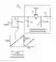
FIG. 1 illustrates one example of an enhanced direct injection circuit 10. The enhanced direct injection circuit 10 utilizes a common gate amplifier similar to that used in direct integration circuits. The enhanced direct injection circuit 10 adds an electronic charge, either as a pulse, constant current, or pulse-shaped current, to the photon-induced charge. The additional charge forces an injection transistor 12 of the common gate amplifier of the enhanced direct injection circuit 10 to provide a low impedance to the photon-induced charge. The additional charge also keeps the injection transistor 12 biased at the end of the integration and allows for near 100% transfer efficiency and high bandwidth.
The enhanced direct injection circuit 10 in FIG. 1 features a detector 14, a first capacitor 16, and a second capacitor 18. The detector 14 may be a photodiode or any other device operable to absorb light. Additionally, the enhanced direct injection circuit 10 features the injection transistor 12 in series with each of the detector 14, first capacitor 16, and second capacitor 18. The injection transistor 12 may be any device operable to amplify or switch electronic signals. A voltage bias is applied to the injection transistor 12 to set an appropriate operating point. A reset switch 20 is also included to periodically reset the enhanced direct injection circuit 10.
A metered or pulse-shaped packet of charge is injected with the photon-induced charge. The magnitude of the voltage supplied over time is illustrated in FIG. 1. The voltage supplied increases linearly with relation to time until the reset switch 20 is applied. After the reset switch 20 is applied, the voltage supplied returns to its original value before increasing linearly again. The additional charge forces the injection transistor 12 of the enhanced direct injection circuit 10 to provide a low impedance to the photon-induced charge.
The charge may be applied in numerous ways. In FIG. 1, the charge is injected through a parallel path using a switching transistor 22 and the second capacitor 18 to the detector 14 through manipulation of the injection gate. In FIG. 2, the charge is injected directly through the detector 14 using the switching transistor 22. In FIG. 3, the charge is injected directly through the detector 14 using two switching transistors 22 and 24 and the second capacitor 18. FIG. 4 illustrates yet another way, similar to FIG. 1 but with an inverse bias, of applying the charge through the parallel path to the detector 14 through manipulation of the injection gate. Other techniques known to those skilled in the art for injecting the charge onto the detector 14 may be used as well. The enhanced direct injection circuit 10 replaces the conventional concept that used an input current source, that had noise and uniformity deficiencies, with a metered or pulse shaped packet of charge that is very uniform and well controlled.
From the foregoing, it may be appreciated by those skilled in the art that a potential technical advantage of some embodiments of the invention is the ability to provide a circuit that is very compact, has low power consumption, has a wide dynamic range at low infrared light levels, and generates a linear response.
Although the present disclosure and its advantages have been described in detail, it should be understood that various changes, substitutions, and alterations can be made therein without departing from the spirit and scope of the disclosure as defined by the appended claims.
Claims
What is claimed is:1. A method of operating a circuit for detector applications, comprising:
adding an electronic charge to a photon-induced charge generated by a detector of a direct injection circuit.
2. The method of claim 1, further comprising:
injecting the electronic charge through a parallel path to the photon-induced charge.
3. The method of claim 1, further comprising:
injecting the electronic charge directly to the photon-induced charge.
4. The method of claim 1, further comprising:
injecting the charge through a capacitor.
5. The method of claim 1, further comprising:
resetting the circuit so that the electronic charge is not added to the photon-induced charge.
6. The method of claim 1, wherein the electronic charge is added to the photon-induced charge as a pulse.
7. The method of claim 1, wherein the electronic charge is added to the photon-induced charge as a constant current.
8. The method of claim 1, wherein the electronic charge is added to the photon-induced charge as a pulse shaped current.
9. A circuit for infrared detection, comprising:
a direct integration circuit operable to generate a photon-induced charge;
a charge injection circuit operable to add an electronic charge to the photon-induced charge.
10. The circuit of claim 9, wherein the charge injection circuit includes a switching transistor and a capacitor to provide a parallel path to add the electronic charge to the photon-induced charge.
11. The circuit of claim 9, wherein the charge injection circuit includes a switching transistor to inject the electronic charge directly to the photon-induced charge.
12. The circuit of claim 9, wherein the charge injection circuit includes a first switching transistor, a capacitor, and a second switching transistor to control injection of the electronic charge to the photon-induced charge.
13. The circuit of claim 9, wherein the direct integration circuit includes a reset transistor to reset the circuit such that the electronic charge is not added to the photon-induced charge.
14. The circuit of claim 9, wherein the electronic charge is added to the photon-induced charge as a pulse.
15. The circuit of claim 9, wherein the electronic charge is added to the photon-induced charge as a constant current.
16. The circuit of claim 9, wherein the electronic charge is added to the photon-induced charge as a pulse shaped current.
Images & Drawings included:

Sources:
- United States Patent and Trademark Office - verify current appl. status at the USPTO↗
Recent applications in this class:
- » 20250211705 2025-06-26
Thermal Imaging Camera - » 20250088604 2025-03-13
IMAGING AND DISPLAY SYSTEM COMBINING IR AND COLOR VIDEO STREAMS - » 20250071233 2025-02-27
Light-Folded Projector - » 20240430380 2024-12-26
SYSTEM AND METHOD FOR PROVISIONING A FACIAL RECOGNITION-BASED SYSTEM FOR CONTROLLING ACCESS TO A BUILDING - » 20240333866 2024-10-03
EVENT-BASED IR CAMERA - » 20240314266 2024-09-19
METHOD FOR DETERMINING HEAT AND REFLECTED HEAT IN THERMAL IMAGE - » 20240236261 2024-07-11
OPTICAL SENSOR HAVING OPAQUE LAYER - » 20240223719 2024-07-04
Mobile gas and chemical imaging camera - » 20240214514 2024-06-27
REFRIGERATION SYSTEM WITH TEMPERATURE MONITORING - » 20240187546 2024-06-06
Uncooled thermal imager
Recent applications for this Assignee:
- » 20250167415 2025-05-22
ENHANCED BROADBAND RING RESONATOR FOR IMPROVED SPECTRAL SUPPRESSION - » 20250145355 2025-05-08
INTEGRATED CABLE PACKAGING, DEPLOYMENT AND STRUMMING MITIGATION SYSTEM - » 20250118501 2025-04-10
MICRO-ELECTROMECHANICAL SYSTEMS SWITCH WITH BEAM MOVEMENT ORTHOGONAL TO FORCE - » 20250116997 2025-04-10
PRODUCT IDENTIFICATION AND TRACKING SYSTEMS AND METHODS - » 20250116851 2025-04-10
REIMAGING LENS ASSEMBLY WITH ANGLED OPTIC - » 20250107006 2025-03-27
RF COVER LAYER - » 20250067792 2025-02-27
DEVICE FOR AND METHOD OF FREQUENCY TESTING PRINTED CIRCUIT BOARD UNDER THERMAL STRESS - » 20250062543 2025-02-20
CONFORMAL WAVEFRONT TRANSFORMER AND METHOD OF MAKING - » 20250035410 2025-01-30
TACTICAL HIGH POWER MICROWAVE ANTENNA PEDESTAL - » 20250027811 2025-01-23
ANTI-BLOOMING BUFFERED DIRECT INJECTION PIXELS