Junction barrier Schottky diode
US20100314708A1
2010-12-16
12/868,346
2010-08-25
✅ Patent granted
US 8,368,166 B2
2013-02-05
-
-
N Drew Richards | John P Dulka
Barnes & Thornburg LLP
2031-08-04
Abstract:
A junction barrier Schottky diode has an N-type well having a surface and a first peak impurity concentration; a P-type anode region in the surface of the well, and having a second peak impurity concentration; an N-type cathode contact region in the surface of the well and laterally spaced from a first wall of the anode region, and having a third peak impurity concentration; and a first N-type region in the surface of the well and laterally spaced from a second wall of the anode region, and having a fourth impurity concentration. The center of the spaced region between the first N-type region and the second wall of the anode region has a fifth peak impurity concentration. An ohmic contact is made to the anode region and cathode contact region, and a Schottky contact is made to the first N-type region. The first and fifth peak impurity concentrations are less than the fourth peak impurity concentration, and the fourth peak impurity concentration is less that the second and third peak impurity concentrations.
Inventors:
- Dev Alok Girdhar 16 🇺🇸 Indialantic, FL, United States
- Michael David Church 11 🇺🇸 Sebastian, FL, United States
Assignee:
- INTERSIL AMERICAS INC. 648 🇺🇸 Milpitas, CA, United States
Applicant:
Interested in similar patents?
Get notified when new applications in this technology area are published.
Classification:
H01L29/66143 » CPC main
Semiconductor devices adapted for rectifying, amplifying, oscillating or switching, or capacitors or resistors with at least one potential-jump barrier or surface barrier, e.g. PN junction depletion layer or carrier concentration layer; Details of semiconductor bodies or of electrodes thereof; Multistep manufacturing processes therefor; Types of semiconductor device ; Multistep manufacturing processes therefor; Multistep manufacturing processes of devices having semiconductor bodies comprising group 14 or group 13/15 materials the devices being controllable only by variation of the electric current supplied or the electric potential applied, to one or more of the electrodes carrying the current to be rectified, amplified, oscillated or switched, e.g. two-terminal devices; Diodes Schottky diodes
H01L29/0692 » CPC further
Semiconductor devices adapted for rectifying, amplifying, oscillating or switching, or capacitors or resistors with at least one potential-jump barrier or surface barrier, e.g. PN junction depletion layer or carrier concentration layer; Details of semiconductor bodies or of electrodes thereof; Multistep manufacturing processes therefor; Semiconductor bodies ; Multistep manufacturing processes therefor characterised by their shape; characterised by the shapes, relative sizes, or dispositions of the semiconductor regions ; characterised by the concentration or distribution of impurities within semiconductor regions characterised by the shape, relative sizes or dispositions of the semiconductor regions or junctions between the regions Surface layout
H01L27/0629 » CPC further
Devices consisting of a plurality of semiconductor or other solid-state components formed in or on a common substrate including semiconductor components specially adapted for rectifying, oscillating, amplifying or switching and having at least one potential-jump barrier or surface barrier; including integrated passive circuit elements with at least one potential-jump barrier or surface barrier the substrate being a semiconductor body including a plurality of individual components in a non-repetitive configuration integrated circuits having a two-dimensional layout of components without a common active region comprising components of the field-effect type in combination with diodes, or resistors, or capacitors
H01L29/872 » CPC further
Semiconductor devices adapted for rectifying, amplifying, oscillating or switching, or capacitors or resistors with at least one potential-jump barrier or surface barrier, e.g. PN junction depletion layer or carrier concentration layer; Details of semiconductor bodies or of electrodes thereof; Multistep manufacturing processes therefor; Types of semiconductor device ; Multistep manufacturing processes therefor controllable only by variation of the electric current supplied, or only the electric potential applied, to one or more of the electrodes carrying the current to be rectified, amplified, oscillated or switched; Diodes Schottky diodes
H01L27/095 IPC
Devices consisting of a plurality of semiconductor or other solid-state components formed in or on a common substrate including semiconductor components specially adapted for rectifying, oscillating, amplifying or switching and having at least one potential-jump barrier or surface barrier; including integrated passive circuit elements with at least one potential-jump barrier or surface barrier the substrate being a semiconductor body including only semiconductor components of a single kind including field-effect components only the components being Schottky barrier gate field-effect transistors
H01L29/47 IPC
Semiconductor devices adapted for rectifying, amplifying, oscillating or switching, or capacitors or resistors with at least one potential-jump barrier or surface barrier, e.g. PN junction depletion layer or carrier concentration layer; Details of semiconductor bodies or of electrodes thereof; Multistep manufacturing processes therefor; Electrodes ; Multistep manufacturing processes therefor characterised by the materials of which they are formed Schottky barrier electrodes
H01L31/07 IPC
Semiconductor devices sensitive to infra-red radiation, light, electromagnetic radiation of shorter wavelength or corpuscular radiation and specially adapted either for the conversion of the energy of such radiation into electrical energy or for the control of electrical energy by such radiation; Processes or apparatus specially adapted for the manufacture or treatment thereof or of parts thereof; Details thereof adapted as photovoltaic [PV] conversion devices characterised by at least one potential-jump barrier or surface barrier the potential barriers being only of the Schottky type
Description
CROSS REFERENCE
The present application is a continuation-in-part to U.S. patent application Ser. No. 12/107,177 filed Apr. 22, 2008 which claims the benefit of U.S. provisional application Ser. No. 60/940,730 filed May 30, 2007 and both of which are incorporated herein by reference.
BACKGROUND AND SUMMARY OF THE DISCLOSURE
The present disclosure relates generally to a junction barrier Schottky diode (JBS) and, more specifically, to a junction barrier Schottky diode with higher reverse blocking voltage.
Integrated circuits have generally included Schottky diodes for power applications. Schottky diodes tend to be very leaky at high reverse bias and high temperatures. Circuit designers have used junction barrier Schottky diodes to provide a solution to the leaky Schottky diodes. This combination provides a Schottky-like forward conduction and PN diode like reverse blocking of voltage. It basically includes a PN junction and a Schottky junction diode in parallel Although this has solved the leakage problems, the JBS diodes built to date have historically had reverse blocking voltages in the range of 30 volts. There is a need to provide an improved JBS diode with substantially greater reverse blocking voltage.
The present junction barrier Schottky diode has an N-type well having a surface and a first peak impurity concentration along a vertical axis; a P-type anode region in the surface of the well, and having a second peak impurity concentration along a vertical axis; an N-type cathode contact region in the surface of the well and laterally spaced from a first wall of the anode region, and having a third peak impurity concentration along a vertical axis; and a first N-type region in the surface of the well and laterally spaced from a second wall of the anode region, and having a fourth peak impurity concentration along a vertical axis. The center of the spaced region between the first N-type region and the second wall of the anode region has a fifth peak impurity concentration along a horizontal axis. An ohmic contact is made to the anode region and the cathode contact region, and a Schottky contact is made to the first N-type region, the spaced region and the well. The first and fifth peak impurity concentrations are less than the fourth peak impurity concentration, and the fourth peak impurity concentration is less that the second and third peak impurity concentrations.
The second peak impurity concentration may be less than the third peak impurity concentration. The spaced region may be the well and the first and fifth peak impurity concentrations are equal. The fifth peak impurity concentration may be less than the first peak impurity concentration, and the fifth peak impurity concentration in the spaced region results from overlap of the anode and the first N-type regions.
The cathode contact, anode and first N-type regions may have substantially the same depth. The cathode contact, anode and first N-type regions may be concentric. One of the cathode contact, anode and first N-type regions may be between two spaced anode or first N-type regions, cathode contact or first N-type regions, and the cathode contact or anode regions respectively may be between two spaced cathode contact regions.
The maximum impurity concentration of the anode and/or the first N-type regions may be below the surface.
Although the junction barrier Schottky diode is generally used in integrated circuits, the present junction barrier Schottky diode may be a discrete device.
These and other aspects of the present disclosure will become apparent from the following detailed description of the disclosure, when considered in conjunction with accompanying drawings.
BRIEF DESCRIPTION OF DRAWINGS
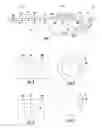
FIG. 1 is cross-sectional view of an integrated circuit including a junction barrier
Schottky diode incorporating the principles of the present disclosure.
FIG. 2 is plain view of a first arrangement of the anode and cathode regions of a junction barrier Schottky diode incorporating the principles of the present disclosure.
FIG. 3 is plain view of a second arrangement of the anode and cathode regions of a junction barrier Schottky diode incorporating the principles of the present disclosure.
FIG. 4 is plain view of a third arrangement of the anode and cathode regions of a junction barrier Schottky diode incorporating the principles of the present disclosure.
FIG. 5 is plain view of a fourth arrangement of the anode and cathode regions of a junction barrier Schottky diode incorporating the principles of the present disclosure.
FIG. 6 is cross-sectional view of a first junction barrier Schottky diode incorporating the principles of the present disclosure.
FIG. 7 is a graph of impurity concentration along cutline 3 of FIG. 6.
FIG. 8 is a graph of impurity concentration along cutline 1 of FIG. 6.
FIG. 9 is a graph of impurity concentration along cutline 2 of FIG. 6.
FIG. 10 is cross-sectional view of a second junction barrier Schottky diode incorporating the principles of the present disclosure.
DETAILED DESCRIPTION OF THE PREFERRED EMBODIMENTS
FIG. 1 illustrates an integrated circuit 10 including a field effect transistor FET 12 and a junction barrier Schottky diode 14. A p-type substrate 16 includes lateral oxide isolation regions 18 offering lateral isolation at the surface between various devices including the FET 12 and the JBS 14. The FET 12 is illustrated as including an N-type source 20 and drain 22 in the P-type substrate 16. A gate 24 is separated from the channel region between the source 20 and the drain 22 by a gate oxide 26. Source contact 28 and drain contact 29 are also shown.
The junction barrier Schottky diode 14 includes an N-type well 30 having a buried N+ layer 32. The upper portion or surface region of the JBS 14 includes an N− region 34. A pair of P-type anode regions 38A and 38B is formed in the surface of region 34. A cathode region 40 laterally adjacent the pair of anode regions 38. The N− region 34 of the well 30 has a lower peak impurity concentration than the peak concentrations of the P anode regions 38 and N cathode region 40. It also has a lower peak impurity concentration than the N well 30. It should be noted that the cathode region 40 has generally the same depth as the anodes 38 such that in the lateral or horizontal direction there is a higher impurity concentration between the anodes 38 A and B while the lower or vertical abutment of the anodes 38A and B is with the lower impurity N− region 34. The plus and minus is to illustrate their relative impurity concentrations. A more detailed explanation of the impurity concentration are illustrated to be discussed below.
Ohmic contacts 42A and 42B are made to the anode region 38A and 38B and a Schottky barrier contact 44 is made with cathode region 40. An N+ cathode contact region 46 extends from the surface to the N+ buried layer 32. An ohmic contact 48 is made to the cathode contact region 46. Materials that form these contacts to produce the appropriate functions are well-known. The cathode region 40 is an active cell partition. The N− region 34 is a lower doped region than the N+ burier layer 32, which carries the current laterally to the cathode. The anode ohmic contacts 42A and 42B and Schottky contact 44 are shown as connected to a common point. This may be by the interconnect structure or by extending the Schottky contact 44 laterally onto the P-region 38 as shown in FIG. 10.
An example of a cross-section of the implementation of the junction barrier Schottky diode 10 is illustrated in FIG. 6. The P-region 38 is ion implanted and is selected to have a peak impurity concentration below the surface of the well 30 as illustrated in FIG. 8. In, the implementation shown, it is generally along the cutline 3 at about 0.5 microns from the surface. The N-region 40 is also formed by ion implantation. The example shown is for a JBS50 which indicates that for the one micron dimension, that the anode and cathode regions of the two parallel diodes are implanted to represent half of the one-micron dimension.
The laterally adjacent the anode region 38 and the cathode region 40 may take various configurations. As previously mentioned, they are generally of the same depth from the surface of the well 30. In one embodiment illustrated in FIG. 2, the cathode region 40 separates to anode region 38A and 38B. As an alternative illustrated in FIG. 3, a single anode region 38 may separate a pair of cathode regions 40A and 40B. The space between the two anode regions 38A and 38B or the two cathode regions 40A and 40B is less than 1 micron and is selected for a specific forward voltage drop and leakage current.
A concentric embodiment is illustrated in FIGS. 4 and 5. In FIG. 4 the cathode region 40 is surrounded by the anode region 38. In FIG. 5 the anode region 38 is surrounded by cathode region 40.
Even though the original implantation of the anode 38 and the cathode 40 are each for half a micron due to other heat steps in the process, the P-type impurities of the anode migrate laterally into the cathode region. FIG. 7 illustrates cutline 3 which is the lateral profile of the impurity concentrations. As will be noted, there is a small region 50 of approximately 0.05 microns where the n and p impurity concentrations of the anode 38 and cathode 40 cancel each other out and as well as the well region 34.
FIG. 8 illustrates at cutline 1, which is from the surface through the anode region 38 into regions 34, 30 and 32. It should be noted at about approximately a half micron below the surface is the peak impurity concentration for the anode region 38. This peak is greater than 1×10¹⁷ carriers per cubic centimeter. The surface cathode region 40 has a peak impurity concentration of just greater than 1×10¹⁶ carriers per cubic centimeter. That is true for FIGS. 7 and 9. Cutline 2 illustrates the specific doping profile for the cathode region 40, and regions 34, 30 and 32. The cathode region may also be formed to have a peak impurity concentration below the surface. The structure shown produces a reverse blocking voltage of least 60 volts.
A modification to the junction barrier Schottky diode of FIGS. 1 and 6 is illustrated in FIG. 10. A P-type anode 38A is surrounded by an N-type cathode 40 which is surrounded by a P-type anode 38B. An N+ cathode contact region 46 surrounds the diode structure. In this structure, the anode regions 38 are spaced from the cathode regions 40 and the cathode contact regions 46 by a surface portion of the N− region 34 of the well. The spacing X at the photo resists or mask level is from 1.0 microns (as shown in FIG. 10) to an overlap of 1 micron (as shown in FIGS. 6 and 7). The maximum impurity concentration in the spaced region is in the center laterally or horizontally. The lateral dimension Y for the cathode regions 40 and the lateral dimension Z for the anode regions 38 are each from 0.5 to 2.0 microns at the mask level.
Although the present disclosure has been described and illustrated in detail, it is to be clearly understood that this is done by way of illustration and example only and is not to be taken by way of limitation. The present junction barrier Schottky diode may also be a discrete device. The scope of the present disclosure is to be limited only by the terms of the appended claims.
Claims
What is claimed:1. A junction barrier Schottky diode, the diode comprising:
an N-type well having a surface and a first peak impurity concentration along a vertical axis;
a P-type anode region in the surface of the well, and having a second peak impurity concentration along a vertical axis;
an N-type cathode contact region in the surface of the well and laterally spaced from a first wall of the anode region, and having a third peak impurity concentration along a vertical axis;
a first N-type region in the surface of the well and laterally spaced from a second wall of the anode region, and having a fourth impurity concentration along a vertical axis;
the center of the spaced region between the first N-type region and the second wall of the anode region having a fifth peak impurity concentration along a horizontal axis;
an ohmic contact to the anode region and cathode contact region, and a Schottky contact to the first N-type region; and
the first and fifth peak impurity concentrations being less than the fourth peak impurity concentration, and the fourth peak impurity concentration being less that the second and third peak impurity concentrations.
2. The diode of claim 1, wherein the second peak impurity concentration is less than the third peak impurity concentration.
3. The diode of claim 1, wherein the spaced region is the well and the first and fifth peak impurity concentrations are equal.
4. The diode of claim 1, wherein the fifth peak impurity concentration is less than the first peak impurity concentration, and the fifth peak impurity concentration in the spaced region results from overlap of the anode and the first N-type regions.
5. The diode of claim 1, wherein the cathode contact region, the anode region and the first N-type region have substantially the same depth.
6. The diode of claim 1, wherein the cathode contact region, the anode region and the first N-type region are concentric.
7. The diode of claim 1, including a spaced pair of one of the wherein the cathode contact region, the anode region and the first N-type region and wherein one of the anode and first N-type regions is between the spaced pair of cathode contact regions, one of the cathode contact region and the first N-type region is between the spaced pair of anode regions, or one of the anode region and the cathode contact region is between the spaced pair of first N-type regions.
8. The diode of claim 1, wherein the peak impurity concentration of the anode region is below the surface.
9. The diode of claim 1, wherein the peak impurity concentration of the first N-type region is below the surface.
10. The diode of claim 1, wherein the first N-type region is formed between two anode regions.
11. The diode of claim 1, including a Schottky contact to the spaced region and the well.
Images & Drawings included:


Sources:
- United States Patent and Trademark Office - verify current appl. status at the USPTO↗
Similar patent applications:
- » 12365083
Schottky barrier diode (SBD) and its off-shoot merged PN/Schottky diode or junction barrier Schottky (JBS) diode - » 20110037139
SCHOTTKY BARRIER DIODE (SBD) AND ITS OFF-SHOOT MERGED PN/SCHOTTKY DIODE OR JUNCTION BARRIER SCHOTTKY (JBS) DIODE - » 20090179297
JUNCTION BARRIER SCHOTTKY DIODE WITH HIGHLY-DOPED CHANNEL REGION AND METHODS - » 20060255423
Silicon carbide junction barrier Schottky diodes with suppressed minority carrier injection - » 17034061
Silicon carbide junction barrier schottky diode with wave-shaped regions - » 20080296722
Junction barrier schottky diode having high reverse blocking voltage - » 20080296587
Silicon carbide semiconductor device having junction barrier Schottky diode - » 20080277668
SIC semiconductor having junction barrier Schottky diode - » 20080296721
Junction barrier Schottky diode with dual silicides - » 20090008651
Silicon carbide semiconductor device having junction barrier schottky diode
Recent applications in this class:
- » 20240258402 2024-08-01
SCHOTTKY BARRIER DIODE WITH REDUCED LEAKAGE CURRENT AND METHOD OF FORMING THE SAME - » 20240162327 2024-05-16
SEMICONDUCTOR STRUCTURE AND METHOD FOR MANUFACTURING SEMICONDUCTOR STRUCTURE - » 20240038870 2024-02-01
SOLUTION-PHASE PROCESSED VERTICAL SCHOTTKY DIODE AND METHOD OF MAKING A VERTICAL SCHOTTKY DIODE - » 20230420539 2023-12-28
ß-Ga2O3 Junction Barrier Schottky (JBS) Diodes with Sputtered p-Type NiO - » 20230326993 2023-10-12
MANUFACTURING METHOD FOR SEMICONDUCTOR ELEMENT, SEMICONDUCTOR ELEMENT, AND SEMICONDUCTOR DEVICE - » 20230137811 2023-05-04
SEMICONDUCTOR DEVICE AND METHOD OF MANUFACTURING SEMICONDUCTOR DEVICE - » 20220367674 2022-11-17
SEMICONDUCTOR DEVICE AND METHOD OF MANUFACTURING SEMICONDUCTOR DEVICE - » 20220310822 2022-09-29
Power device and method for making the same - » 20220285524 2022-09-08
Schottky barrier diode with reduced leakage current and method of forming the same - » 20210202716 2021-07-01
Schottky barrier diode with reduced leakage current and method of forming the same
Recent applications for this Assignee:
- » 20150035504 2015-02-05
Switching regulator input current sensing circuit, system, and method - » 20140210655 2014-07-31
Sigma-delta converter system and method - » 20140206300 2014-07-24
Methods and systems for noise and interference cancellation - » 20140157015 2014-06-05
Clamp circuits for power converters - » 20140113444 2014-04-24
Active area bonding compatible high current structures - » 20140007927 2014-01-09
Switchable solar cell devices - » 20130285628 2013-10-31
Integrated power supply with wide input supply voltage range - » 20130223550 2013-08-29
Discrete multi-tone systems for half-duplex IP links - » 20130221380 2013-08-29
Optoelectronic apparatuses with post-molded reflector cups and methods for manufacturing the same - » 20130214133 2013-08-22
Configurable photo detector circuit