Activation treatments in plating processes
US20110287628A1
2011-11-24
12/784,314
2010-05-20
✅ Patent granted
US 8,703,546 B2
2014-04-22
-
-
Matthew Landau | Igwe U Anya
Slater & Matsil, L.L.P.
2031-10-28
Abstract:
A method of forming a device includes performing a first plating process to form a first metallic feature, and performing an activation treatment to a surface of the first metallic feature in an activation treatment solution, wherein the activation treatment solution includes a treatment agent in de-ionized (DI) water. After the step of performing the activation treatment, performing a second plating process to form a second metallic feature and contacting the surface of the first metallic feature.
Inventors:
- Ming-Da Cheng 238 🇹🇼 Jhubei City, Taiwan
- Chih-Wei Lin 42 🇹🇼 Xinfeng Township, Taiwan
- Chung-Shi LIU 50 🇹🇼 Shin-Chu, Taiwan
- Ming-Che HO 103 🇹🇼 Tainan City, Taiwan
- Ming-Da Cheng 238 🇹🇼 Jhubei, Taiwan
- Ming-Che Ho 92 🇹🇼 Tainan, Taiwan
Assignee:
- TAIWAN SEMICONDUCTOR MANUFACTURING COMPANY, LTD. 8,890 🇹🇼 Hsin-Chu, Taiwan
Applicant:
Interested in similar patents?
Get notified when new applications in this technology area are published.
Classification:
H01L21/288 » CPC main
Processes or apparatus adapted for the manufacture or treatment of semiconductor or solid state devices or of parts thereof; Manufacture or treatment of semiconductor devices or of parts thereof the devices having at least one potential-jump barrier or surface barrier, e.g. PN junction, depletion layer or carrier concentration layer the devices having semiconductor bodies comprising elements of Group IV of the Periodic System or AB compounds with or without impurities, e.g. doping materials; Manufacture of electrodes on semiconductor bodies using processes or apparatus not provided for in groups -; Deposition of conductive or insulating materials for electrodes conducting electric current from a liquid, e.g. electrolytic deposition
C25D7/123 » CPC further
Electroplating characterised by the article coated; Semiconductors Semiconductors first coated with a seed layer or a conductive layer
H01L24/11 » CPC further
Arrangements for connecting or disconnecting semiconductor or solid-state bodies; Methods or apparatus related thereto; Means for bonding being attached to, or being formed on, the surface to be connected, e.g. chip-to-package, die-attach, "first-level" interconnects; Manufacturing methods related thereto; Bump connectors ; Manufacturing methods related thereto Manufacturing methods
H01L24/13 » CPC further
Arrangements for connecting or disconnecting semiconductor or solid-state bodies; Methods or apparatus related thereto; Means for bonding being attached to, or being formed on, the surface to be connected, e.g. chip-to-package, die-attach, "first-level" interconnects; Manufacturing methods related thereto; Bump connectors ; Manufacturing methods related thereto; Structure, shape, material or disposition of the bump connectors prior to the connecting process of an individual bump connector
H01L24/03 » CPC further
Arrangements for connecting or disconnecting semiconductor or solid-state bodies; Methods or apparatus related thereto; Means for bonding being attached to, or being formed on, the surface to be connected, e.g. chip-to-package, die-attach, "first-level" interconnects; Manufacturing methods related thereto; Bonding areas ; Manufacturing methods related thereto Manufacturing methods
H01L24/05 » CPC further
Arrangements for connecting or disconnecting semiconductor or solid-state bodies; Methods or apparatus related thereto; Means for bonding being attached to, or being formed on, the surface to be connected, e.g. chip-to-package, die-attach, "first-level" interconnects; Manufacturing methods related thereto; Bonding areas ; Manufacturing methods related thereto; Structure, shape, material or disposition of the bonding areas prior to the connecting process of an individual bonding area
H01L2224/0345 » CPC further
Indexing scheme for arrangements for connecting or disconnecting semiconductor or solid-state bodies and methods related thereto as covered by; Means for bonding being attached to, or being formed on, the surface to be connected, e.g. chip-to-package, die-attach, "first-level" interconnects; Manufacturing methods related thereto; Bonding areas; Manufacturing methods related thereto; Manufacturing methods by blanket deposition of the material of the bonding area in gaseous form Physical vapour deposition [PVD], e.g. evaporation, or sputtering
H01L2224/03831 » CPC further
Indexing scheme for arrangements for connecting or disconnecting semiconductor or solid-state bodies and methods related thereto as covered by; Means for bonding being attached to, or being formed on, the surface to be connected, e.g. chip-to-package, die-attach, "first-level" interconnects; Manufacturing methods related thereto; Bonding areas; Manufacturing methods related thereto; Manufacturing methods; Post-treatment of the bonding area; Reworking, e.g. shaping involving a chemical process, e.g. etching the bonding area
H01L2224/0401 » CPC further
Indexing scheme for arrangements for connecting or disconnecting semiconductor or solid-state bodies and methods related thereto as covered by; Means for bonding being attached to, or being formed on, the surface to be connected, e.g. chip-to-package, die-attach, "first-level" interconnects; Manufacturing methods related thereto; Bonding areas; Manufacturing methods related thereto; Structure, shape, material or disposition of the bonding areas prior to the connecting process Bonding areas specifically adapted for bump connectors, e.g. under bump metallisation [UBM]
H01L2224/11424 » CPC further
Indexing scheme for arrangements for connecting or disconnecting semiconductor or solid-state bodies and methods related thereto as covered by; Means for bonding being attached to, or being formed on, the surface to be connected, e.g. chip-to-package, die-attach, "first-level" interconnects; Manufacturing methods related thereto; Bump connectors; Manufacturing methods related thereto; Manufacturing methods by blanket deposition of the material of the bump connector in liquid form Immersion coating, e.g. in a solder bath
H01L2224/11462 » CPC further
Indexing scheme for arrangements for connecting or disconnecting semiconductor or solid-state bodies and methods related thereto as covered by; Means for bonding being attached to, or being formed on, the surface to be connected, e.g. chip-to-package, die-attach, "first-level" interconnects; Manufacturing methods related thereto; Bump connectors; Manufacturing methods related thereto; Manufacturing methods by blanket deposition of the material of the bump connector; Plating Electroplating
H01L2224/11464 » CPC further
Indexing scheme for arrangements for connecting or disconnecting semiconductor or solid-state bodies and methods related thereto as covered by; Means for bonding being attached to, or being formed on, the surface to be connected, e.g. chip-to-package, die-attach, "first-level" interconnects; Manufacturing methods related thereto; Bump connectors; Manufacturing methods related thereto; Manufacturing methods by blanket deposition of the material of the bump connector; Plating Electroless plating
H01L2224/11622 » CPC further
Indexing scheme for arrangements for connecting or disconnecting semiconductor or solid-state bodies and methods related thereto as covered by; Means for bonding being attached to, or being formed on, the surface to be connected, e.g. chip-to-package, die-attach, "first-level" interconnects; Manufacturing methods related thereto; Bump connectors; Manufacturing methods related thereto; Manufacturing methods by patterning a pre-deposited material using masks Photolithography
H01L2224/1181 » CPC further
Indexing scheme for arrangements for connecting or disconnecting semiconductor or solid-state bodies and methods related thereto as covered by; Means for bonding being attached to, or being formed on, the surface to be connected, e.g. chip-to-package, die-attach, "first-level" interconnects; Manufacturing methods related thereto; Bump connectors; Manufacturing methods related thereto; Manufacturing methods; Post-treatment of the bump connector Cleaning, e.g. oxide removal step, desmearing
H01L2924/01006 » CPC further
Indexing scheme for arrangements or methods for connecting or disconnecting semiconductor or solid-state bodies as covered by; Chemical elements Carbon [C]
H01L2924/01013 » CPC further
Indexing scheme for arrangements or methods for connecting or disconnecting semiconductor or solid-state bodies as covered by; Chemical elements Aluminum [Al]
H01L2924/01029 » CPC further
Indexing scheme for arrangements or methods for connecting or disconnecting semiconductor or solid-state bodies as covered by; Chemical elements Copper [Cu]
H01L2924/0103 » CPC further
Indexing scheme for arrangements or methods for connecting or disconnecting semiconductor or solid-state bodies as covered by; Chemical elements Zinc [Zn]
H01L2924/01032 » CPC further
Indexing scheme for arrangements or methods for connecting or disconnecting semiconductor or solid-state bodies as covered by; Chemical elements Germanium [Ge]
H01L2924/01033 » CPC further
Indexing scheme for arrangements or methods for connecting or disconnecting semiconductor or solid-state bodies as covered by; Chemical elements Arsenic [As]
H01L2924/01047 » CPC further
Indexing scheme for arrangements or methods for connecting or disconnecting semiconductor or solid-state bodies as covered by; Chemical elements Silver [Ag]
H01L2924/01072 » CPC further
Indexing scheme for arrangements or methods for connecting or disconnecting semiconductor or solid-state bodies as covered by; Chemical elements Hafnium [Hf]
H01L2924/01073 » CPC further
Indexing scheme for arrangements or methods for connecting or disconnecting semiconductor or solid-state bodies as covered by; Chemical elements Tantalum [Ta]
H01L2924/01074 » CPC further
Indexing scheme for arrangements or methods for connecting or disconnecting semiconductor or solid-state bodies as covered by; Chemical elements Tungsten [W]
H01L2924/01079 » CPC further
Indexing scheme for arrangements or methods for connecting or disconnecting semiconductor or solid-state bodies as covered by; Chemical elements Gold [Au]
H01L2924/01082 » CPC further
Indexing scheme for arrangements or methods for connecting or disconnecting semiconductor or solid-state bodies as covered by; Chemical elements Lead [Pb]
H01L2924/01322 » CPC further
Indexing scheme for arrangements or methods for connecting or disconnecting semiconductor or solid-state bodies as covered by; Alloys; Binary Alloys Eutectic Alloys, i.e. obtained by a liquid transforming into two solid phases
H01L2924/01327 » CPC further
Indexing scheme for arrangements or methods for connecting or disconnecting semiconductor or solid-state bodies as covered by; Alloys; Binary Alloys Intermediate phases, i.e. intermetallics compounds
H01L2924/014 » CPC further
Indexing scheme for arrangements or methods for connecting or disconnecting semiconductor or solid-state bodies as covered by; Alloys Solder alloys
H01L2924/10329 » CPC further
Indexing scheme for arrangements or methods for connecting or disconnecting semiconductor or solid-state bodies as covered by; Details of semiconductor or other solid state devices to be connected; Material of the semiconductor or solid state bodies; Semiconducting materials; Compound semiconductors; III-V Gallium arsenide [GaAs]
H01L2224/93 » CPC further
Indexing scheme for arrangements for connecting or disconnecting semiconductor or solid-state bodies and methods related thereto as covered by Batch processes
H01L2224/11 » CPC further
Indexing scheme for arrangements for connecting or disconnecting semiconductor or solid-state bodies and methods related thereto as covered by; Means for bonding being attached to, or being formed on, the surface to be connected, e.g. chip-to-package, die-attach, "first-level" interconnects; Manufacturing methods related thereto; Bump connectors; Manufacturing methods related thereto Manufacturing methods
H01L2224/13099 » CPC further
Indexing scheme for arrangements for connecting or disconnecting semiconductor or solid-state bodies and methods related thereto as covered by; Means for bonding being attached to, or being formed on, the surface to be connected, e.g. chip-to-package, die-attach, "first-level" interconnects; Manufacturing methods related thereto; Bump connectors; Manufacturing methods related thereto; Structure, shape, material or disposition of the bump connectors prior to the connecting process of an individual bump connector; Core members of the bump connector Material
H01L2224/13599 » CPC further
Indexing scheme for arrangements for connecting or disconnecting semiconductor or solid-state bodies and methods related thereto as covered by; Means for bonding being attached to, or being formed on, the surface to be connected, e.g. chip-to-package, die-attach, "first-level" interconnects; Manufacturing methods related thereto; Bump connectors; Manufacturing methods related thereto; Structure, shape, material or disposition of the bump connectors prior to the connecting process of an individual bump connector; Coating Material
H01L2224/05599 » CPC further
Indexing scheme for arrangements for connecting or disconnecting semiconductor or solid-state bodies and methods related thereto as covered by; Means for bonding being attached to, or being formed on, the surface to be connected, e.g. chip-to-package, die-attach, "first-level" interconnects; Manufacturing methods related thereto; Bonding areas; Manufacturing methods related thereto; Structure, shape, material or disposition of the bonding areas prior to the connecting process of an individual bonding area; External layer Material
H01L2224/05099 » CPC further
Indexing scheme for arrangements for connecting or disconnecting semiconductor or solid-state bodies and methods related thereto as covered by; Means for bonding being attached to, or being formed on, the surface to be connected, e.g. chip-to-package, die-attach, "first-level" interconnects; Manufacturing methods related thereto; Bonding areas; Manufacturing methods related thereto; Structure, shape, material or disposition of the bonding areas prior to the connecting process of an individual bonding area; Internal layers Material
H01L2224/29099 » CPC further
Indexing scheme for arrangements for connecting or disconnecting semiconductor or solid-state bodies and methods related thereto as covered by; Means for bonding being attached to, or being formed on, the surface to be connected, e.g. chip-to-package, die-attach, "first-level" interconnects; Manufacturing methods related thereto; Layer connectors, e.g. plate connectors, solder or adhesive layers; Manufacturing methods related thereto; Structure, shape, material or disposition of the layer connectors prior to the connecting process of an individual layer connector; Core members of the layer connector Material
H01L2924/00013 » CPC further
Indexing scheme for arrangements or methods for connecting or disconnecting semiconductor or solid-state bodies as covered by; Technical content checked by a classifier Fully indexed content
H01L2224/29599 » CPC further
Indexing scheme for arrangements for connecting or disconnecting semiconductor or solid-state bodies and methods related thereto as covered by; Means for bonding being attached to, or being formed on, the surface to be connected, e.g. chip-to-package, die-attach, "first-level" interconnects; Manufacturing methods related thereto; Layer connectors, e.g. plate connectors, solder or adhesive layers; Manufacturing methods related thereto; Structure, shape, material or disposition of the layer connectors prior to the connecting process of an individual layer connector; Coating Material
H01L2924/0002 » CPC further
Indexing scheme for arrangements or methods for connecting or disconnecting semiconductor or solid-state bodies as covered by; Technical content checked by a classifier Not covered by any one of groups , and
H01L2924/14 » CPC further
Indexing scheme for arrangements or methods for connecting or disconnecting semiconductor or solid-state bodies as covered by; Details of semiconductor or other solid state devices to be connected; Device type Integrated circuits
H01L2924/00 » CPC further
Indexing scheme for arrangements or methods for connecting or disconnecting semiconductor or solid-state bodies as covered by
H01L2224/11901 » CPC further
Indexing scheme for arrangements for connecting or disconnecting semiconductor or solid-state bodies and methods related thereto as covered by; Means for bonding being attached to, or being formed on, the surface to be connected, e.g. chip-to-package, die-attach, "first-level" interconnects; Manufacturing methods related thereto; Bump connectors; Manufacturing methods related thereto; Manufacturing methods; Methods of manufacturing bump connectors involving a specific sequence of method steps with repetition of the same manufacturing step
H01L2224/1146 » CPC further
Indexing scheme for arrangements for connecting or disconnecting semiconductor or solid-state bodies and methods related thereto as covered by; Means for bonding being attached to, or being formed on, the surface to be connected, e.g. chip-to-package, die-attach, "first-level" interconnects; Manufacturing methods related thereto; Bump connectors; Manufacturing methods related thereto; Manufacturing methods by blanket deposition of the material of the bump connector Plating
H01L21/445 IPC
Processes or apparatus adapted for the manufacture or treatment of semiconductor or solid state devices or of parts thereof; Manufacture or treatment of semiconductor devices or of parts thereof the devices having at least one potential-jump barrier or surface barrier, e.g. PN junction, depletion layer or carrier concentration layer the devices having semiconductor bodies not provided for in groups, , , and with or without impurities, e.g. doping materials; Manufacture of electrodes on semiconductor bodies using processes or apparatus not provided for in groups - ; Deposition of conductive or insulating materials for electrodes from a liquid, e.g. electrolytic deposition
H01L21/82 IPC
Processes or apparatus adapted for the manufacture or treatment of semiconductor or solid state devices or of parts thereof; Manufacture or treatment of devices consisting of a plurality of solid state components formed in or on a common substrate or of parts thereof; Manufacture of integrated circuit devices or of parts thereof; Manufacture or treatment of devices consisting of a plurality of solid state components or integrated circuits formed in, or on, a common substrate with subsequent division of the substrate into plural individual devices to produce devices, e.g. integrated circuits, each consisting of a plurality of components
Description
TECHNICAL FIELD
This disclosure relates generally to integrated circuits, and more particularly to plating processes, and even more particularly to bump formation processes using plating processes.
BACKGROUND
In the formation of a semiconductor chip, integrated circuit devices, such as transistors, are first formed at the surface of a semiconductor substrate in the semiconductor chip. Interconnect structures are then formed over the integrated circuit devices. Bumps are formed on the surface of the semiconductor chip so that the integrated circuit devices can be accessed.
In a typical bump formation process, an under-bump metallurgy (UBM) is formed, followed by the formation of a bump on the UBM. The UBM formation may include forming a copper seed layer and forming and patterning a mask on the copper seed layer so that a portion of the copper seed layer is exposed through an opening in the mask. A plating step is then performed to plate a thick copper layer on the exposed portion of the copper seed layer. Subsequently, additional layers, such as a nickel layer and a solder layer may be plated successively. Conventionally, between each of the plating processes, a quick dump rinse (QDR) is performed using de-ionized (DI) water to clean the surfaces of the plated layers.
It was found that the interfaces between the plated layers were rough, with voids formed therein. As a consequence, the electro-migration (EM) performance, and hence the reliability, of the resulting bumps is degraded.
SUMMARY
In accordance with one aspect, a method of forming a device includes performing a first plating process to form a first metallic feature, and performing an activation treatment to a surface of the first metallic feature in an activation treatment solution, wherein the activation treatment solution includes a treatment agent in de-ionized (DI) water. After the step of performing the activation treatment, performing a second plating process to form a second metallic feature and contacting the surface of the first metallic feature.
Other embodiments are also disclosed.
BRIEF DESCRIPTION OF THE DRAWINGS
For a more complete understanding of the embodiments, and the advantages thereof, reference is now made to the following descriptions taken in conjunction with the accompanying drawings, in which:
FIGS. 1 through 7 are cross-sectional views of intermediate stages in the manufacturing of a metal bump in accordance with an embodiment; and
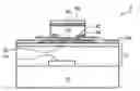
FIG. 8 illustrates an activation treatment process performed on a wafer.
DETAILED DESCRIPTION OF ILLUSTRATIVE EMBODIMENTS
The making and using of the embodiments of the disclosure are discussed in detail below. It should be appreciated, however, that the embodiments provide many applicable inventive concepts that can be embodied in a wide variety of specific contexts. The specific embodiments discussed are merely illustrative and do not limit the scope of the disclosure.
A novel integrated circuit formation process is provided in accordance with an embodiment. The intermediate stages of manufacturing an embodiment are illustrated. The variations of the embodiment are discussed. Throughout the various views and illustrative embodiments, like reference numbers are used to designate like elements.
Referring to FIG. 1, wafer 2, which includes substrate 10, is provided. Substrate 10 may be a semiconductor substrate, such as a bulk silicon substrate, although it may include other semiconductor materials, such as silicon germanium, silicon carbide, gallium arsenide, or the like. Semiconductor devices 14, such as transistors, may be formed at the surface of substrate 10. Interconnect structure 12, which includes metal lines and vias (not shown) formed therein and connected to semiconductor devices 14, is formed over substrate 10. The metal lines and vias may be formed of copper or copper alloys and may be formed using the well-known damascene processes. Interconnect structure 12 may include inter-layer dielectrics (ILDs) and inter-metal dielectrics (IMDs). In alternative embodiments, wafer 2 is an interposer wafer or a package substrate, and is substantially free from integrated circuit devices, including devices, such as transistors, resistors, capacitors, inductors, and/or the like formed therein. In these embodiments, substrate 10 may be formed of a semiconductor material or a dielectric material, such as silicon oxide.
Metal pad 28 is formed over interconnect structure 12. Metal pad 28 may comprise aluminum, copper (Cu), silver (Ag), gold (Au), nickel (Ni), tungsten (W), alloys thereof, and/or multi-layers thereof. Metal pad 28 may be electrically coupled to semiconductor devices 14, for example, through the underlying interconnection structure 12. Passivation layer 30 may be formed to cover edge portions of metal pad 28. In an exemplary embodiment, passivation layer 30 is formed of polyimide or other known dielectric materials, such as silicon oxide, silicon nitride, and multi-layers thereof.
Referring to FIG. 2, an under-bump metallurgy (UBM), which may include diffusion barrier layer 40 (which is optional) and seed layer 42, is blanket formed. Diffusion barrier layer 40 may be a titanium layer, a titanium nitride layer, a tantalum layer, or a tantalum nitride layer. The materials of seed layer 42 may include copper or copper alloys, and hence is alternatively referred to as copper seed layer 42 hereinafter. However, other metals, such as silver, gold, aluminum, and combinations thereof, may also be included. In an embodiment, diffusion barrier layer 40 and copper seed layer 42 are formed using physical vapor deposition or other applicable methods.
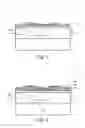
FIG. 3 illustrates the formation of mask 46, which may be formed of a photo resist, for example. Accordingly, copper seed layer 42 is exposed through opening 45 in mask 46. Next, wafer 2 is placed into a plating solution (not shown), and a plating is performed to form first metallic feature 50 on UBM 40/42 and opening 45, as shown in FIG. 4. The plating may be an electro-plating, an electroless-plating, an immersion plating, or the like. In an embodiment, first metallic layer 50 is a copper layer or a copper alloy layer.
Referring to FIG. 8, after the formation of first metallic layer 50, an activation treatment is performed. In an embodiment, activation treatment solution 52, as shown in FIG. 8, comprises de-ionized (DI) water and additional additives dissolved therein. The additives may include a treatment agent, such as an acid or other chemicals, that may activate and clean the surface of first metallic layer 50. In an exemplary embodiment, the treatment agent in activation treatment solution 52 comprises CX100, which may comprise about 30% citric acid (C6H8O7). The treatment agent may also comprise HF, oxalic acid, HNO3, HCl, NH4OH, H2SO4, and/or the like. The weight percentage of the treatment agent may range between about 1 percent to about 40 percent. In the activation treatment, a temperature of treatment solution 52 may be between about 25° C. and about 50° C. During the activation treatment, the surface of first metallic layer 50 is cleaned, and any oxide, such as copper oxide, at the surface of first metallic layer 50 is removed.
Next, as shown in FIG. 5, second metallic layer 54 is formed on the surface of first metallic layer 50, wherein the formation method may also be an electro-plating, an electroless-plating, an immersion plating, or the like. In an exemplary embodiment, second metallic layer 54 is a nickel layer. Next, a second activation treatment is performed on the surface of second metallic layer 54 in an activation treatment solution, which may be essentially the same as treatment solution 52 shown in FIG. 8. Similarly, the second activation treatment has the function of activating and cleaning the surface of second metallic layer 54 and removing oxide from the surface of second metallic layer 54.
FIG. 6 illustrates the formation of third metallic layer 60 on the surface of second metallic layer 54, with the formation method including one of the electro-plating, electroless-plating, and immersion plating. Third metallic layer 60 may be a solder layer, which may be an eutectic solder or a lead-free solder. In an exemplary embodiment, the solder of third metallic layer 60 comprises zinc, silver, and copper, although other elements may also be used. Next, a third activation treatment is performed on the surface of third metallic layer 60 in an activation treatment solution, which may be essentially the same as the treatment solution 52 shown in FIG. 8.
After the formation of third metallic layer 60, mask 46 is removed, and the portion of UBM 40/42 previously covered by mask 46 is also removed, for example, by an etch. The resulting structure is shown in FIG. 7.
It is realized that although the exemplary embodiments use the formation of metal bumps on the surface of a substrate as examples, the teaching is readily applicable to plating processes for forming other metallic features.
Experiments have shown that by using the embodiments, the interfaces between different layers are significantly improved, and a significant reduction in voids has been observed. Further, the interfaces become much smoother. As a result, the electro-migration (EM) performance, and hence the reliability, of the resulting metal bumps is also improved over conventional metal bumps that are formed with quick dump rinse (QDR) between plating processes.
Although the embodiments and their advantages have been described in detail, it should be understood that various changes, substitutions, and alterations can be made herein without departing from the spirit and scope of the embodiments as defined by the appended claims. Moreover, the scope of the present application is not intended to be limited to the particular embodiments of the process, machine, manufacture, and composition of matter, means, methods and steps described in the specification. As one of ordinary skill in the art will readily appreciate from the disclosure, processes, machines, manufacture, compositions of matter, means, methods, or steps, presently existing or later to be developed, that perform substantially the same function or achieve substantially the same result as the corresponding embodiments described herein may be utilized according to the disclosure. Accordingly, the appended claims are intended to include within their scope such processes, machines, manufacture, compositions of matter, means, methods, or steps. In addition, each claim constitutes a separate embodiment, and the combination of various claims and embodiments are within the scope of the disclosure.
Claims
What is claimed is:1. A method of forming a device comprising:
performing a first plating process to form a first metallic feature;
performing a first activation treatment to a surface of the first metallic feature in a first activation treatment solution comprising a first treatment agent in de-ionized (DI) water; and
after the step of performing the first activation treatment, performing a second plating process to form a second metallic feature and contacting the surface of the first metallic feature.
2. The method of claim 1, wherein the first treatment agent comprises an acid.
3. The method of claim 2, wherein the first treatment agent comprises CX100 comprising citric acid (C6H8O7).
4. The method of claim 1, wherein a weight percentage of the first treatment agent in the first activation treatment solution is between about 1 percent and about 40 percent.
5. The method of claim 1, wherein the first metallic feature is a copper layer, and the second metallic feature is a nickel layer.
6. The method of claim 1 further comprising:
after the step of performing the second plating process, performing a second activation treatment to a surface of the second metallic feature in a second activation treatment solution comprising a second treatment agent in DI water; and
after the step of performing the second activation treatment, performing a third plating process to form a third metallic feature contacting the surface of the second metallic feature.
7. The method of claim 6, wherein the first metallic feature is a copper layer, the second metallic feature is a nickel layer, and the third metallic feature is a solder layer.
8. The method of claim 6, wherein the first, the second, and the third metallic features form a metal bump at a surface of a wafer comprising integrated circuits therein.
9. The method of claim 1, wherein the first and the second plating processes are selected from the group consisting essentially of electro-plating, electroless-plating, and immersion plating.
10. A method of forming a device comprising:
providing a substrate;
forming an under-bump metallurgy (UBM) over the substrate;
forming and patterning a mask over the UBM, with a portion of the UBM exposed through an opening in the mask;
performing a first plating process to form a copper layer over the portion of the UBM exposed through the opening;
performing a first activation treatment to a surface of the copper layer in a first activation treatment solution comprising a treatment agent in de-ionized (DI) water;
after the step of performing the first activation treatment, performing a second plating process to form a nickel layer on the surface of the copper layer;
after the step of performing the second plating process, performing a second activation treatment to a surface of the nickel layer in a second activation treatment solution comprising the treatment agent in DI water; and
after the step of performing the second activation treatment, performing a third plating process to form a solder layer on the surface of the nickel layer.
11. The method of claim 10, wherein the treatment agent comprises citric acid (C6H8O7).
12. The method of claim 10, wherein weight percentages of the treatment agent in the first and the second activation treatment solutions are between about 1 percent and about 40 percent.
13. The method of claim 10 further comprising:
after the step of performing the third plating process, performing a third activation treatment to a surface of the solder layer in a third activation treatment solution comprising the treatment agent in DI water; and
removing the mask and portions of the UBM directly under the mask.
14. The method of claim 10, wherein the first, the second, and the third plating processes are selected from the group consisting essentially of electro-plating, electroless-plating plating, and immersion plating.
15. A method of forming a device comprising:
providing a substrate;
forming an under-bump metallurgy (UBM) over the substrate;
forming and patterning a mask over the UBM, with a portion of the UBM exposed through an opening in the mask;
performing a first plating process to form a copper layer over the portion of the UBM exposed through the opening; and
performing a first activation treatment to a surface of the copper layer in a first activation treatment solution comprising a treatment agent in de-ionized (DI) water, wherein the treatment agent comprises CX100 comprising citric acid (C6H8O7).
16. The method of claim 15 further comprising:
after the step of performing the first activation treatment, performing a second plating process to form a nickel layer on the surface of the copper layer; and
after the step of performing the second plating process, performing a second activation treatment to a surface of the nickel layer in a second activation treatment solution comprising the treatment agent in DI water.
17. The method of claim 16 further comprising, after the step of performing the second activation treatment, performing a third plating process to form a solder layer on the surface of the nickel layer.
18. The method of claim 15, wherein a weight percentage of the treatment agent in the first activation treatment solution is between about 1 percent and about 40 percent.
19. The method of claim 15, wherein during the first activation treatment, a temperature of the first activation treatment solution is between about 25° C. and about 50° C.
Images & Drawings included:


Sources:
- United States Patent and Trademark Office - verify current appl. status at the USPTO↗
Recent applications in this class:
- » 20250201565 2025-06-19
Electroless Deposition Process for Semiconductor Devices - » 20250038004 2025-01-30
CONDUCTIVE MATERIAL DEPOSITION ON SEMICONDUCTOR WITH PHASE TRANSITION AND OHMIC CONTACT IN SITU - » 20240222129 2024-07-04
METHOD AND DEVICE FOR FILLING A REAR-SIDE CAVITY OF A SEMICONDUCTOR ASSEMBLY - » 20230326758 2023-10-12
SEMICONDUCTOR DEVICE AND METHOD FOR MANUFACTURING THE SAME - » 20220406605 2022-12-22
SUBSTRATE LIQUID PROCESSING METHOD AND SUBSTRATE LIQUID PROCESSING APPARATUS - » 20220319854 2022-10-06
SELECTIVE DEPOSITION USING HYDROLYSIS - » 20220310397 2022-09-29
Method of forming an electrically conductive feature traversing a microscopic step and related apparatus - » 20210175083 2021-06-10
METHOD OF MANUFACTURING METAL ELECTRODE - » 20210005460 2021-01-07
Selective deposition using hydrolysis - » 20200357644 2020-11-12
Semiconductor device manufacturing method
Recent applications for this Assignee:
- » 20240266341 2024-08-08
HYBRID BONDING WITH UNIFORM PATTERN DENSITY - » 20240224489 2024-07-04
SEMICONDUCTOR DEVICE - » 20240170063 2024-05-23
CONTENT ADDRESSABLE MEMORY ARRAY DEVICE STRUCTURE - » 20240161819 2024-05-16
MEMORY DEVICE AND MANUFACTURING THEREOF - » 20240153896 2024-05-09
SEMICONDUCTOR PACKAGE SYSTEM AND METHOD - » 20240120409 2024-04-11
Method for non-resist nanolithography - » 20240113080 2024-04-04
Semiconductor Device with Discrete Blocks - » 20240105632 2024-03-28
Method for forming a semiconductor device including forming a first interconnect structure on one side of a substrate having first metal feature closer the substrate than second metal feature and forming first and second tsv on other side of substrate connecting to the metal features - » 20240096816 2024-03-21
Method of manufacture overlay mark using laser marking process for semiconductor device - » 20240096383 2024-03-21
MEMORY DEVICE