Encapsulating method for sealed and water-proof LED and luminescent holder
US20120106172A1
2012-05-03
12/915,058
2010-10-29
Abstract:
This invention relates to an encapsulating method for sealed and water-proof LED, comprising the following steps: separately weld two leads or three leads onto the two pins of the LED; molding by mould and used for installing the holder of LED; put the LED with lead or various types of ornaments into the holder; buckle the holder; weld the periphery of the buckled holder by ultrasonic machine to form a sealed luminescent light. By means of welding the lead of the luminotron first, putting it into the holder later, and finally sealing it by ultrasonic machine, it can increase the up-to-standard rate and reduce the rejections on the premise of ensuring the sealing effect.
Interested in similar patents?
Get notified when new applications in this technology area are published.
Classification:
H01L33/52 » CPC main
Semiconductor devices with at least one potential-jump barrier or surface barrier specially adapted for light emission; Processes or apparatus specially adapted for the manufacture or treatment thereof or of parts thereof; Details thereof characterised by the semiconductor body packages Encapsulations
B29C39/10 » CPC further
Shaping by casting, i.e. introducing the moulding material into a mould or between confining surfaces without significant moulding pressure; Apparatus therefor for making articles of definite length, i.e. discrete articles incorporating preformed parts or layers, e.g. casting around inserts or for coating articles
H01L2933/005 » CPC further
Details relating to devices covered by the group but not provided for in its subgroups; Processes relating to semiconductor body packages relating to encapsulations
H01L2224/13099 » CPC further
Indexing scheme for arrangements for connecting or disconnecting semiconductor or solid-state bodies and methods related thereto as covered by; Means for bonding being attached to, or being formed on, the surface to be connected, e.g. chip-to-package, die-attach, "first-level" interconnects; Manufacturing methods related thereto; Bump connectors; Manufacturing methods related thereto; Structure, shape, material or disposition of the bump connectors prior to the connecting process of an individual bump connector; Core members of the bump connector Material
H01L2224/13599 » CPC further
Indexing scheme for arrangements for connecting or disconnecting semiconductor or solid-state bodies and methods related thereto as covered by; Means for bonding being attached to, or being formed on, the surface to be connected, e.g. chip-to-package, die-attach, "first-level" interconnects; Manufacturing methods related thereto; Bump connectors; Manufacturing methods related thereto; Structure, shape, material or disposition of the bump connectors prior to the connecting process of an individual bump connector; Coating Material
H01L2224/05599 » CPC further
Indexing scheme for arrangements for connecting or disconnecting semiconductor or solid-state bodies and methods related thereto as covered by; Means for bonding being attached to, or being formed on, the surface to be connected, e.g. chip-to-package, die-attach, "first-level" interconnects; Manufacturing methods related thereto; Bonding areas; Manufacturing methods related thereto; Structure, shape, material or disposition of the bonding areas prior to the connecting process of an individual bonding area; External layer Material
H01L2224/05099 » CPC further
Indexing scheme for arrangements for connecting or disconnecting semiconductor or solid-state bodies and methods related thereto as covered by; Means for bonding being attached to, or being formed on, the surface to be connected, e.g. chip-to-package, die-attach, "first-level" interconnects; Manufacturing methods related thereto; Bonding areas; Manufacturing methods related thereto; Structure, shape, material or disposition of the bonding areas prior to the connecting process of an individual bonding area; Internal layers Material
H01L2224/29099 » CPC further
Indexing scheme for arrangements for connecting or disconnecting semiconductor or solid-state bodies and methods related thereto as covered by; Means for bonding being attached to, or being formed on, the surface to be connected, e.g. chip-to-package, die-attach, "first-level" interconnects; Manufacturing methods related thereto; Layer connectors, e.g. plate connectors, solder or adhesive layers; Manufacturing methods related thereto; Structure, shape, material or disposition of the layer connectors prior to the connecting process of an individual layer connector; Core members of the layer connector Material
H01L2924/00013 » CPC further
Indexing scheme for arrangements or methods for connecting or disconnecting semiconductor or solid-state bodies as covered by; Technical content checked by a classifier Fully indexed content
H01L2224/29599 » CPC further
Indexing scheme for arrangements for connecting or disconnecting semiconductor or solid-state bodies and methods related thereto as covered by; Means for bonding being attached to, or being formed on, the surface to be connected, e.g. chip-to-package, die-attach, "first-level" interconnects; Manufacturing methods related thereto; Layer connectors, e.g. plate connectors, solder or adhesive layers; Manufacturing methods related thereto; Structure, shape, material or disposition of the layer connectors prior to the connecting process of an individual layer connector; Coating Material
H01L33/48 IPC
Semiconductor devices with at least one potential-jump barrier or surface barrier specially adapted for light emission; Processes or apparatus specially adapted for the manufacture or treatment thereof or of parts thereof; Details thereof characterised by the semiconductor body packages
H01L21/50 IPC
Processes or apparatus adapted for the manufacture or treatment of semiconductor or solid state devices or of parts thereof; Manufacture or treatment of semiconductor devices or of parts thereof the devices having at least one potential-jump barrier or surface barrier, e.g. PN junction, depletion layer or carrier concentration layer Assembly of semiconductor devices using processes or apparatus not provided for in a single one of the subgroups - , e.g. sealing of a cap to a base of a container
Description
BACKGROUND OF THE INVENTION
This invention relates to the method of making string lights by LED, specifically relates to an encapsulating method for sealed and water-proof LED and luminescent light made by this method.
In prior art, there is a luminescent string lights. Each luminescent light is composed of LED and holder. Generally, it is switched into conduction after connecting the pin of the luminotron and the shrapnel in the holder. The shrapnel is connected to the power through lead. Since the string lights are normally used outside, the holder is not water-proof and the pin and the shrapnel are not fixed together, the LED may be poor in conductance or damaged if water enters the holder.
There is another method that is to directly encapsulate the LED and the holder together by means of one-off injection moulding. Although this method is water-proof, the rate of finished products is low and the amount of rejections increases.
BRIEF SUMMARY OF THE INVENTION
The objective of the present invention is to overcome the shortcomings in existing technology and to provide an encapsulating method for sealed and water-proof LED and luminescent light. The luminescent light made by this method is low in cost and rejections. Moreover, it is superior in water-proof performance and will not be damaged even though it is used outside for a long time.
Provide an encapsulating method for sealed and water-proof LED, including the following steps:
Separately weld two leads or three leads onto the two pins of the LED;
Molding by mould and used for installing the holder of LED;
Put the LED with lead or various types of ornaments into the holder;
Buckle the holder;
Weld the periphery of the buckled holder by ultrasonic machine to form a sealed luminescent light.
This invention enjoys such advantages as the followings: By means of welding the lead of the luminotron first, putting it into the holder later, and finally sealing it by ultrasonic machine, it can increase the up-to-standard rate and reduce the rejections on the premise of ensuring the sealing effect.
The holder can adopt folding structure which is to set a folding structure on one side only. It can also use two same hemi-structures which have buckle structure. The pin of the LED can be directly welded on the holder. Its luminescent end comes out from one end of the holder after installing the LED. The other two or three leads separately come out from the two holes of the other end, and then the periphery of the two hemi-components is welded together by the ultrasonic plastic soldering technique, so as to form a complete sealed holder. In this way, the rain could not immerge into it. As the LED and the lead are directly welded, damage by immerged water and poor conductance are avoided.
BRIEF DESCRIPTION OF THE DRAWINGS
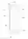
FIG. 1 is the structure profile of one hemi-structure in Implementation Example One of holder of sealed and water-proof luminescent light made by this method.
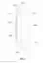
FIG. 2 is lateral view of FIG. 1.
FIG. 3 is structure chart of sealed and water-proof luminescent holder.
DETAILED DESCRIPTION OF THE INVENTION
Provide an encapsulating method for sealed and water-proof LED, including the following steps: separately weld two leads or three leads onto the two pins of the LED; molding by mould and used for installing the holder of LED; put the LED with lead or various types of ornaments into the holder; buckle the holder; weld the periphery of the buckled holder by ultrasonic machine to form a sealed luminescent light.
As shown in FIGS. 1, 2 and 3, it provides a sealed and water-proof luminescent holder which is composed of two hemi-components 1 buckled together. After the two hemi-components buckled together, there forms a chamber inside. One end forms a hole for inserting the LED and the other end forms two separate holes for the two or three leads of the LED to get through.
As shown in FIG. 1, the two hemi-components 1 are structured in semi-column whose inside is a cavity 101. One end is a semicircular orifice 102 and the other end is two small separate semicircular orifices 103. One lateral surface of the semi-column is equipped with a strip 104 which is set with one bayoner lock 105 separately on its two ends. The other lateral surface is installed with slot 106 and hole 107 for said strip 104 and bayoner lock 105. The two hemi-components form a column holder after connected by the strip 104 and slot 106 and bayoner lock 105 and hole 107.
The periphery of the two hemi-components is welded together by the ultrasonic plastic soldering technique, so as to form a complete sealed holder. In this way, the rain could not immerge into it. As the LED and the lead are directly welded, damage by immerged water and poor conductance are avoided.
Claims
What is claimed is:1. An encapsulating method for sealed and water-proof LED, comprising the following steps:
1) separately weld two leads or three leads onto the two pins of the LED;
2) molding by mould and used for installing the holder of LED;
3) put the LED with lead or various types of ornaments into the holder;
4) buckle the holder;
5) Weld the periphery of the buckled holder by ultrasonic machine to form a sealed luminescent light.
2. A sealed and water-proof luminescent holder adopting the method as set forth in claim 1, characterized in that it is composed by two hemi-components buckled together; after the two hemi-components buckled together, there forms a chamber inside; one end forms a hole for inserting the LED and the other end forms two separate holes for the two or three leads of the LED to get through.
3. The sealed and water-proof luminescent holder as set forth in claim 2, characterized in that the said hemi-component is structured in semi-column whose inside is a cavity; on one end is a semicircular orifice and on the other end are two small separate semicircular orifices; one lateral surface of the semi-column is equipped with a strip which is set with one bayoner lock separately on its two ends; the other lateral surface is installed with slot and hole for said strip and bayoner lock; the two hemi-components form a column holder after connected by the strip and bayoner lock.
Images & Drawings included:


Sources:
- United States Patent and Trademark Office - verify current appl. status at the USPTO↗
Recent applications in this class:
- » 20250056937 2025-02-13
ETCHED TRENCHES IN BOND MATERIALS FOR DIE SINGULATION, AND ASSOCIATED SYSTEMS AND METHODS - » 20250022991 2025-01-16
SEMICONDUCTOR PACKAGE - » 20240421269 2024-12-19
HIDDEN DISPLAY DEVICE AND METHOD OF MANUFACTURING THE SAME - » 20240266480 2024-08-08
METHOD OF MANUFACTURING LIGHT-EMITTING DEVICE INCLUDING STEP OF CURING SEALING MEMBER WHILE APPLYING CENTRIFUGAL FORCE - » 20240258472 2024-08-01
DISPLAY DEVICE AND MANUFACTURING METHOD THEREOF - » 20240250221 2024-07-25
Semiconductor package and manufacturing method of semiconductor package - » 20240234649 2024-07-11
LIGHT EMITTING DEVICE - » 20240170621 2024-05-23
DISPLAY DEVICE - » 20240136479 2024-04-25
LIGHT EMITTING DEVICE - » 20240097083 2024-03-21
Light emitting device having a dam surrounding a light emitting region and a barrier surrounding the dam