Up-conversion device with broad band absorber
US20120217477A1
2012-08-30
13/272,928
2011-10-13
✅ Patent granted
US 8,592,801 B2
2013-11-26
-
-
Ha Tran T Nguyen | Dzung Tran
Wolf, Greenfield & Sacks, P.C.
2032-01-05
Abstract:
Embodiments of the invention are directed to an IR photodetector that broadly absorbs electromagnetic radiation including at least a portion of the near infrared (NIR) spectrum. The IR photodetector comprises polydispersed QDs of PbS and/or PbSe. The IR photodetector can be included as a layer in an up-conversion device when coupled to a light emitting diode (LED) according to an embodiment of the invention.
Inventors:
- FRANKY SO 39 🇺🇸 Gainesville, FL, United States
- Do Young Kim 16 🇺🇸 Gainesville, FL, United States
- Bhabendra Pradhan 6 🇺🇸 Marietta, GA, United States
- Jae Woong Lee 4 🇺🇸 Gainesville, FL, United States
Assignee:
- UNIVERSITY OF FLORIDA RESEARCH FOUNDATION, INC. 1,575 🇺🇸 Gainesville, FL, United States
- NanoHoldings LLC 20 🇺🇸 Rowayton, CT, United States
Applicant:
Interested in similar patents?
Get notified when new applications in this technology area are published.
Classification:
H01L51/426 » CPC main
Solid state devices using organic materials as the active part, or using a combination of organic materials with other materials as the active part; Processes or apparatus specially adapted for the manufacture or treatment of such devices, or of parts thereof specially adapted for sensing infra-red radiation, light, electro-magnetic radiation of shorter wavelength or corpuscular radiation and adapted for the conversion of the energy of such radiation into electrical energy or for the control of electrical energy by such radiation using organic materials as the active part, or using a combination of organic materials with other material as the active part; Multistep processes for their manufacture comprising bulk hetero-junctions, e.g. interpenetrating networks comprising inorganic nanostructures, e.g. CdSe nanoparticles
B82Y30/00 » CPC further
Nanotechnology for materials or surface science, e.g. nanocomposites
H01L51/50 » CPC further
Solid state devices using organic materials as the active part, or using a combination of organic materials with other materials as the active part; Processes or apparatus specially adapted for the manufacture or treatment of such devices, or of parts thereof specially adapted for light emission, e.g. organic light emitting diodes [OLED] or polymer light emitting devices [PLED]
H01L2251/5369 » CPC further
Indexing scheme relating to organic semiconductor devices covered by group; Organic light emitting devices; Structure Nanoparticles used in whatever layer except emissive layer, e.g. in packaging
Y02E10/549 » CPC further
Energy generation through renewable energy sources; Photovoltaic [PV] energy Organic PV cells
Y02E10/549 » CPC further
Energy generation through renewable energy sources; Photovoltaic [PV] energy Organic PV cells
H01L51/44 IPC
Solid state devices using organic materials as the active part, or using a combination of organic materials with other materials as the active part; Processes or apparatus specially adapted for the manufacture or treatment of such devices, or of parts thereof specially adapted for sensing infra-red radiation, light, electro-magnetic radiation of shorter wavelength or corpuscular radiation and adapted for the conversion of the energy of such radiation into electrical energy or for the control of electrical energy by such radiation using organic materials as the active part, or using a combination of organic materials with other material as the active part; Multistep processes for their manufacture Details of devices
B82Y15/00 IPC
Nanotechnology for interacting, sensing or actuating, e.g. quantum dots as markers in protein assays or molecular motors
H01L31/00 IPC
Semiconductor devices sensitive to infra-red radiation, light, electromagnetic radiation of shorter wavelength or corpuscular radiation and specially adapted either for the conversion of the energy of such radiation into electrical energy or for the control of electrical energy by such radiation; Processes or apparatus specially adapted for the manufacture or treatment thereof or of parts thereof; Details thereof
H01L29/08 IPC
Semiconductor devices adapted for rectifying, amplifying, oscillating or switching, or capacitors or resistors with at least one potential-jump barrier or surface barrier, e.g. PN junction depletion layer or carrier concentration layer; Details of semiconductor bodies or of electrodes thereof; Multistep manufacturing processes therefor; Semiconductor bodies ; Multistep manufacturing processes therefor characterised by their shape; characterised by the shapes, relative sizes, or dispositions of the semiconductor regions ; characterised by the concentration or distribution of impurities within semiconductor regions with semiconductor regions connected to an electrode carrying current to be rectified, amplified or switched and such electrode being part of a semiconductor device which comprises three or more electrodes
H01L33/00 IPC
Semiconductor devices with at least one potential-jump barrier or surface barrier specially adapted for light emission; Processes or apparatus specially adapted for the manufacture or treatment thereof or of parts thereof; Details thereof
Description
CROSS-REFERENCE TO RELATED APPLICATION
The present application claims the benefit of U.S. Provisional Application Ser. No. 61/447,427, filed Feb. 28, 2011, which is hereby incorporated by reference herein in its entirety, including any figures, tables, or drawings.
BACKGROUND OF INVENTION
Recently, light up-conversion devices have attracted a great deal of research interest because of their potential applications in night vision, range finding, and security, as well as semiconductor wafer inspections. Early near infrared (NIR) up-conversion devices were mostly based on the heterojunction structure of inorganic semiconductors where a photodetecting and a luminescent section are in series. The up-conversion devices are mainly distinguished by the method of photodetection. Up-conversion efficiencies of devices are typically very low. For example, one NIR-to-visible light up-conversion device that integrates a light-emitting diode (LED) with a semiconductor based photodetector exhibits a maximum external conversion efficiency of only 0.048 (4.8%) W/W. A hybrid organic/inorganic up-conversion device, where an InGaAs/InP photodetector is coupled to an organic light-emitting diode (OLED), exhibits an external conversion efficiency of 0.7% W/W. Currently inorganic and hybrid up-conversion devices are expensive to fabricate and the processes used for fabricating these devices are not compatible with large area applications. Efforts are being made to achieve low cost up-conversion devices that have higher conversion efficiencies, although no device has been identified that allows sufficient efficiency to be considered a practical up-conversion device. For some applications, such as night vision devices, up-conversion devices having an IR sensitizing layer with a broad absorption spectrum is very desirable.
BRIEF SUMMARY
Embodiments of the invention are directed to an IR photodetector comprising a cathode, an anode, and an IR sensitizing layer, comprising polydispersed quantum dots (QDs), that absorbs over a broad range, including at least a portion of the near infrared (NIR). The QD layer comprises polydispersed PbS QDs and/or polydispersed PbSe QDs that comprise either a polymodal mixture of different sized monodispersed QDs, a monomodal polydispersed QD mixture, or a polymodal polydispersed QD mixture. The polydispersed quantum dots (QDs) can be synthesized directly or prepared by mixing a plurality of different sized QDs. The IR photodetector can include a hole blocking layer (HBL) and/or an electron blocking layer (EBL).
In other embodiments of the invention, an up-conversion device is formed by the combination of the IR photodetector and a light emitting diode (LED). The LED comprises a light emitting layer and optionally an electron transport layer (ETL) and/or a hole transport layer (HTL).
BRIEF DESCRIPTION OF DRAWINGS
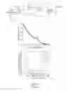
FIG. 1 shows a) a schematic energy band diagram of a prior art infrared-to-visible light up-conversion device with single absorption peak spectrum, b) an absorbance spectrum of an IR absorbing PbSe quantum dot (QD) film with monodispersed QDs, and c) a plot of the photon-to-photon conversion efficiency of the up-conversion device.
FIG. 2 shows composite of absorbance spectra for a PbSe quantum dot film having different sized monodispersed QDs.
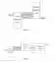
FIG. 3 shows a) an up-conversion device with an IR sensitizing layer of mixed QDs and b) the absorbance spectra of a polydispersed PbSe QD film that would result from the combination of the three monodispersed QDs of the films of FIG. 2.
FIG. 4 shows absorption spectra for polydispersed PbS QDs prepared with different metal to calcogenide ratios at a) 160° C. and b) 140° C. and c) an up-conversion device with an IR sensitizing layer of polydispersed QDs according to an embodiment of the invention.
FIG. 5 shows a schematic energy band diagram of a photodetector comprising a broad absorption IR sensitizing layer comprising polydispersed QDs according to an embodiment of the invention.
FIG. 6 shows a schematic energy band diagram of an up-conversion device with an IR sensitizing layer of polydispersed quantum dots according to an embodiment of the invention
DETAILED DISCLOSURE
Embodiments of the invention are directed to devices having an infrared (IR) sensitizing layer having a broad absorption spectrum comprising polydispersed quantum dots (QDs). The IR sensitizing layer can be used in an IR photodetector that can be used in an IR up-conversion device, according to embodiments of the invention. FIG. 1a is a schematic diagram of a prior art up-conversion device having an IR sensitizing layer. The device uses a film of monodispersed PbSe quantum dots as the IR sensitizing layer with an absorption maximum of about 1300 nm, as can be seen in the spectrum shown in FIG. 1b, to provide the energy input for the photodetector. FIG. 1c shows the photon-to-photon conversion efficiency of the IR up-conversion device. The conversion efficiency spectrum of the up-conversion device reflects the absorbance spectrum of the PbSe quantum dot film.
The absorption spectra of PbSe quantum dots depend on the size of PbSe quantum dots, as shown in FIG. 2, where the spectra of three different sized PbSe QDs are superimposed with their longest wavelength maximum normalized to one absorbance unit. According to an embodiment of the invention, an up-conversion device includes an IR photodetector that comprises a sensitizing layer of polydispersed PbSe QDs of different sizes and a light emitting diode (LED). As illustrated, for either up-conversion device in FIG. 3a, by having a polymodal combination of three monodispersed QDs of the different sizes, which individually display the absorbance spectra of FIG. 2, a combined absorbance spectrum results, as indicated in FIG. 3b. Rather than combining different available monodispersed QDs, a monomodal polydispersed QDs mixture can be synthesized. In this manner, many different sized QDs are present as a continuum of sizes rather than as a mixture of discrete sizes. FIGS. 4a and 4b show broad absorption spectra for films of polydispersed PbS QDs that could be included in an IR photosensitizing layer in an up-conversion device, for example, as illustrated in FIG. 4c. By controlling the molar proportions of the metal and calcogenide reagents and the reaction temperature, QDs with broad absorptions are possible. As shown in FIGS. 4a and 4b, PbS QDs with absorption maxima at 1320 nm and 1150 nm are formed at a Pb:S ratio of 1:1.5 at 160° C. and 140° C., respectively, while increasing the S ratio results in the formation of PbS QD with broader absorption spectra at 160° C. and 140° C., with the broadest spectrum observed for the QDs prepared at a Pb:S ratio of 1:4 at 160° C. These QDs absorb in a portion of the near IR (NIR) with absorbance extending into the visual. As can be appreciated by those skilled in the art, any monomodal mixture of polydispersed QDs, any mixture of polydispersed QDs with monodispersed QDs, any mixture of a plurality of different monodispersed QDs, or any polymodal mixture of polydispersed QDs can be prepared to provide a broad absorbing IR sensitizing layer according to embodiments of the invention.
FIG. 5 is the schematic energy band diagram of a photodetector comprising a broad absorption IR sensitizing layer, according to an embodiment of the invention. In FIG. 5, an optional electron blocking layer (EBL) and an optional hole blocking layer (HBL) are included in the photodetector. The broad absorption IR sensitizing layer can comprise mixed PbSe QDs or mixed PbS QDs. The optional HBL can be an organic HBL comprising, for example, 2,9-Dimethyl-4,7-diphenyl-1,10-phenanthroline (BCP), p-bis(triphenylsilyl)benzene (UGH2), 4,7-diphenyl-1,10-phenanthroline (BPhen), tris-(8-hydroxy quinoline) aluminum (Alq3), 3,5′-N,N′-dicarbazole-benzene (mCP), C60, or tris[3-(3-pyridyl)-mesityl]borane (3TPYMB). The optional HBL can be an inorganic HBL, for example a HBL comprising ZnO or TiO2. The optional EBL can be 1,1-bis[(di-4-tolylamino)phenyl]cyclohexane (TAPC), N,N′-diphenyl-N,N′(2-naphthyl)-(1,1′-phenyl)-4,4′-diamine (NPB), and N,N′-diphenyl-N,N′-di(m-tolyl) benzidine (TPD).
FIG. 6 is the schematic energy band diagram of an infrared-to-visible light up-conversion device having an IR photodetector that comprises a broad absorption IR sensitizing layer, according to an embodiment of the invention. As shown in FIG. 6, the anode can be, but is not limited to: Indium tin Oxide (ITO), Indium Zinc Oxide (IZO), Aluminum Tin Oxide (ATO), Aluminum Zinc Oxide (AZO) or carbon nanotubes. Electroluminescent light emitting diode (LED) materials that can be employed include, but are not limited to, tris-(2-phenylpyidine) iridium (Ir(ppy)3), poly-[2-methoxy, 5-(2′-ethyl-hexyloxy) phenylene vinylene] (MEH-PPV), tris-(8-hydroxy quinoline) aluminum (Alq3), and iridium (III) bis-[(4,6-di-fluorophenyl)-pyridinate-N,C2′]picolinate (FIrpic). The cathode can be LiF/Al or can be any conductor with the appropriate work function including, but not limited to, Ag, Ca, Mg, LiF/Al/ITO, Ag/ITO, CsCO3/ITO and Ba/Al. The device can include a hole transport layer (HTL). Materials that can be employed as a HTL include, but are not limited to, 1,1-bis[(di-4-tolylamino)phenyl]cyclohexane (TAPC), N,N′-diphenyl-N,N′(2-naphthyl)-(1,1′-phenyl)-4,4′-diamine (NPB), and N,N′-diphenyl-N,N′-di(m-tolyl) benzidine (TPD). The device can include an electron transport layer (ETL). Materials that can be employed as an ETL include, but are not limited to, tris[3-(3-pyridyl)-mesityl]borane (3TPYMB), 2,9-Dimethyl-4,7-diphenyl-1,10-phenanthroline (BCP), 4,7-diphenyl-1,10-phenanthroline (BPhen), and tris-(8-hydroxy quinoline) aluminum (Alq3). Those skilled in the art can readily identify appropriate combinations of anodes, cathodes, LED materials, optional HTLs, optional HBLs, optional EBLs and optional ETLs that can be employed with the IR sensitizing layer of by their relative work functions, HOMO and LUMO levels, layer compatibility, and the nature of any desired deposition methods used during their fabrication of devices according to embodiments of the invention.
Methods and Materials
Polydispersed PbSe nanocrystals were synthesized using diphenylphosphine (DPP) as a catalyst. In a typical reaction, lead oxide (2 mmol) was dissolved in a mixture of octadecene and oleic acid (6 mmol) with uniform heating and vigorous stirring under an argon atmosphere. When the temperature reached 140° C., 6 mmol of 1M selenium in trioctylphospine and 56 μl of DPP were rapidly injected into the lead comprising solution to initiate the nucleation of nanocrystals. The size of the nanocrystals depends on the reaction composition, reaction temperature, and reaction time. The reaction was terminated by injection of cold toluene to the reaction mixture. The resulting nanocrystals were subsequently isolated by: precipitating with acetone; redispersing the nanocrystals in toluene; and repeating the steps of precipitating and redispersing three times to remove excess unreacted precursors and reaction byproducts.
Subsequently, a ligand exchange reaction was carried out where the bulky oleate ligands were exchanged with shorter-chain octylamine or ethanethiol ligands in a nitrogen glove box over a period of 48 hours, where: after precipitating the nanocrystals in acetone, the nanocrystals were redispersed in 10 ml of octylamine; or, after redispersing the nanocrystals in toluene, an equal volume of ethanethiol was added to the suspension. Subsequently, the ligand exchanged particles were precipitated with acetone and finally redispersed in chloroform at a concentration of about 60 mg/ml. The exchange of oleate passivating groups with octylamine resulted in a clear dispersion with no agglomeration of particles.
All patents, patent applications, provisional applications, and publications referred to or cited herein are incorporated by reference in their entirety, including all figures and tables, to the extent they are not inconsistent with the explicit teachings of this specification.
It should be understood that the examples and embodiments described herein are for illustrative purposes only and that various modifications or changes in light thereof will be suggested to persons skilled in the art and are to be included within the spirit and purview of this application.
Claims
We claim:1. An IR photodetector, comprising: a cathode; an anode; and an IR sensitizing layer comprising polydispersed quantum dots (QDs), wherein the IR sensitizing layer absorbs over a broad range including at least a portion of the near infrared (NIR).
2. The photodetector of claim 1, wherein the IR sensitizing layer comprises polydispersed PbS QDs and/or polydispersed PbSe QDs.
3. The photodetector of claim 1, wherein the polydispersed QDs comprise a polymodal mixture of monodispersed QDs, a monomodal polydispersed QD mixture, or a polymodal polydispersed QD mixture.
4. The IR photodetector of claim 1, wherein the cathode comprises Ag, Ca, Mg, Indium tin Oxide (ITO), Indium Zinc Oxide (IZO), Aluminum Tin Oxide (ATO), Aluminum Zinc Oxide (AZO), carbon nanotube, silver nanowire, LiF/Al/ITO, Ag/ITO, or CsCO3/ITO.
5. The IR photodetector of claim 1, wherein the anode comprises Ag, Ca, Mg, Indium tin Oxide (ITO), Indium Zinc Oxide (IZO), Aluminum Tin Oxide (ATO), Aluminum Zinc Oxide (AZO), carbon nanotube, silver nanowire, LiF/Al/ITO, Ag/ITO, and CsCO3/ITO.
6. The IR photodetector of claim 1, further comprising a hole blocking layer (HBL) and/or an electron blocking layer (EBL).
7. The IR photodetector of claim 6, wherein the HBL comprises 2,9-Dimethyl-4,7-diphenyl-1,10-phenanthroline (BCP), p-bis(triphenylsilyl)benzene (UGH2), 4,7-diphenyl-1,10-phenanthroline (BPhen), tris-(8-hydroxy quinoline) aluminum (Alq3), 3,5′-N,N′-dicarbazole-benzene (mCP), C60, tris[3-(3-pyridyl)-mesityl]borane (3TPYMB), ZnO, or TiO2.
8. The IR photodetector of claim 6, wherein the EBL of claim 6 comprises 1,1-bis[(di-4-tolylamino)phenyl]cyclohexane (TAPC), N,N′-diphenyl-N,N′(2-naphthyl)-(1,1′-phenyl)-4,4′-diamine (NPB), and N,N′-diphenyl-N,N′-di(m-tolyl) benzidine (TPD).
9. An up-conversion device, comprising the IR photodetector of claim 1 and a light emitting diode (LED).
10. The up-conversion device of claim 9, wherein the LED comprises a light emitting layer.
11. The up-conversion device of claim 10, wherein the light emitting layer comprises tris-(2-phenylpyidine) iridium (Ir(ppy)3), poly-[2-methoxy, 5-(2′-ethyl-hexyloxy) phenylene vinylene] (MEH-PPV), tris-(8-hydroxy quinoline) aluminum (Alq3), or iridium (III) bis-[(4,6-di-fluorophenyl)-pyridinate-N,C2′]picolinate (FIrpic).
12. The up-conversion device of claim 9, wherein the LED further comprises an electron transport layer (ETL) and/or a hole transport layer (HTL)
13. The up-conversion device of claim 12, wherein the ETL comprises tris[3-(3-pyridyl)-mesityl]borane (3TPYMB), 2,9-Dimethyl-4,7-diphenyl-1,10-phenanthroline (BCP), 4,7-diphenyl-1,10-phenanthroline (BPhen), or tris-(8-hydroxy quinoline) aluminum (Alq3).
14. The up-conversion device of claim 12, wherein the HTL comprises 1,1-bis[(di-4-tolylamino)phenyl]cyclohexane (TAPC), N,N′-diphenyl-N,N′(2-naphthyl)-(1,1′-phenyl)-4,4′-diamine (NPB), or N,N′-diphenyl-N,N′-di(m-tolyl) benzidine (TPD).
Images & Drawings included:


Sources:
- United States Patent and Trademark Office - verify current appl. status at the USPTO↗
Recent applications in this class:
- » 20220255026 2022-08-11
LIGHT ABSORPTION LAYER AND MANUFACTURING METHOD THEREFOR, PHOTOELECTRIC CONVERSION ELEMENT, AND INTERMEDIATE-BAND SOLAR CELL - » 20220231242 2022-07-21
Composite interface transport material-based perovskite photovoltaic, light emission and light detection multi-functional device and preparation method therefor - » 20220216438 2022-07-07
Photodetectors based on two-dimensional quantum dots - » 20220115610 2022-04-14
PHOTODETECTOR ELEMENT, MANUFACTURING METHOD FOR PHOTODETECTOR ELEMENT, IMAGE SENSOR, DISPERSION LIQUID, AND SEMICONDUCTOR FILM - » 20210313531 2021-10-07
Photoelectric conversion element that reduces a residual image while enhancing heat resistance - » 20210296602 2021-09-23
Donor-acceptor interfaces for excitonic semiconductors - » 20200328365 2020-10-15
VEHICLE LAMPS - » 20200144524 2020-05-07
Photovoltaic cells based on donor and acceptor nano-particulate conjugates in conductive polymer blends - » 20200091450 2020-03-19
Organic electronic device and manufacturing method thereof - » 20200083469 2020-03-12
Mid and far-infrared nanocrystals based photodetectors with enhanced performances
Recent applications for this Assignee:
- » 20250050487 2025-02-13
COMPACT MECHANICAL WAVEGUIDES FOR IMPACT DEVICES - » 20250002542 2025-01-02
Insect Toxin Delivery Mediated by a Begomovirus Coat Protein - » 20240287652 2024-08-29
HIGH TEMPERATURE LIGHTWEIGHT AL-FE-SI BASED ALLOYS - » 20240237951 2024-07-18
HEART RATE MEASUREMENT USING ADAPTIVE HARMONICS FILTERING - » 20240187735 2024-06-06
Acoustic Eavesdropping Using A Smartphone Camera - » 20240184001 2024-06-06
Systems and methods for detecting sources of particle emissions - » 20240162859 2024-05-16
SELF-AMPLIFIED RESONATORS WITH EMBEDDED PIEZORESISTIVE ELEMENTS FOR HIGH PERFORMANCE, ULTRA-LOW SW AP MICROWAVE AND MILLIMETER-WAVE APPLICATIONS - » 20240104364 2024-03-28
MEMRISTIVE NANOFIBER NEURAL NETWORKS - » 20240092738 2024-03-21
N,N diethyl-N'phenylpiperazine alpha 7 and alpha 9 nicotinic acetylcholine receptor agonists and antagonists - » 20240084521 2024-03-14
Waste to energy ash and engineered aggregate in road construction