Multilevel resistive memory having large storage capacity
US20130069031A1
2013-03-21
13/513,155
2012-02-08
✅ Patent granted
US 8,633,465 B2
2014-01-21
WO; PCT/CN2012/070952; 20120208
WO; WO2013/037195; 20130321
Mark A Laurenzi
DLA Piper LLP US
2032-02-08
Abstract:
The present invention discloses a multilevel resistive memory having large storage capacity, which belongs to a field of a fabrication technology of a resistive memory. The resistive memory includes an top electrode and a bottom electrode, and a combination of a plurality of switching layers and defective layers interposed between the top electrode and the bottom electrode, wherein, the top electrode and the bottom electrode are respectively contacted with a switching layer (a film such as Ta2O5, TiO2, HfO2), and the defective layers (metal film such as Ti, Au, Ag) are interposed between the switching layers. By using the present invention, a storage capacity of a resistive memory can be increased.
Inventors:
- Ru Huang 95 🇨🇳 Beijing, China
- Gengyu Yang 6 🇨🇳 Beijing, China
- Yimao Cai 30 🇨🇳 Beijing, China
- Yu Tang 16 🇨🇳 Beijing, China
- Lijie Zhang 92 🇨🇳 Beijing, China
- Yue Pan 40 🇨🇳 Beijing, China
- Shenghu Tan 6 🇨🇳 Beijing, China
- Yinglong Huang 33 🇨🇳 Beijing, China
Assignee:
- PEKING UNIVERSITY 458 🇨🇳 Beijing, China
- PEKING UNIVERSITY NO. 5 YIHEYUAN ROAD HAIDIAN DISTRICT 1 🇨🇳 Beijing, China
Applicant:
Interested in similar patents?
Get notified when new applications in this technology area are published.
Classification:
H01L45/08 » CPC main
Solid state devices adapted for rectifying, amplifying, oscillating or switching without a potential-jump barrier or surface barrier, e.g. dielectric triodes; Ovshinsky-effect devices; Processes or apparatus peculiar to the manufacture or treatment thereof or of parts thereof; Bistable or multistable switching devices, e.g. for resistance switching non-volatile memory based on migration or redistribution of ionic species, e.g. anions, vacancies
G11C11/5685 » CPC further
Digital stores characterised by the use of particular electric or magnetic storage elements; Storage elements therefor using storage elements with more than two stable states represented by steps, e.g. of voltage, current, phase, frequency using storage elements comprising metal oxide memory material, e.g. perovskites
H01L45/12 » CPC further
Solid state devices adapted for rectifying, amplifying, oscillating or switching without a potential-jump barrier or surface barrier, e.g. dielectric triodes; Ovshinsky-effect devices; Processes or apparatus peculiar to the manufacture or treatment thereof or of parts thereof; Bistable or multistable switching devices, e.g. for resistance switching non-volatile memory Details
H01L45/1233 » CPC further
Solid state devices adapted for rectifying, amplifying, oscillating or switching without a potential-jump barrier or surface barrier, e.g. dielectric triodes; Ovshinsky-effect devices; Processes or apparatus peculiar to the manufacture or treatment thereof or of parts thereof; Bistable or multistable switching devices, e.g. for resistance switching non-volatile memory; Details; Device geometry adapted for essentially vertical current flow, e.g. sandwich or pillar type devices
H01L45/146 » CPC further
Solid state devices adapted for rectifying, amplifying, oscillating or switching without a potential-jump barrier or surface barrier, e.g. dielectric triodes; Ovshinsky-effect devices; Processes or apparatus peculiar to the manufacture or treatment thereof or of parts thereof; Bistable or multistable switching devices, e.g. for resistance switching non-volatile memory; Selection of switching materials; Oxides or nitrides Binary metal oxides, e.g. TaOx
G11C13/0007 » CPC further
Digital stores characterised by the use of storage elements not covered by groups , , or using resistive RAM [RRAM] elements comprising metal oxide memory material, e.g. perovskites
H01L45/00 IPC
Solid state devices adapted for rectifying, amplifying, oscillating or switching without a potential-jump barrier or surface barrier, e.g. dielectric triodes; Ovshinsky-effect devices; Processes or apparatus peculiar to the manufacture or treatment thereof or of parts thereof
H01L47/00 IPC
Bulk negative resistance effect devices, e.g. Gunn-effect devices; Processes or apparatus peculiar to the manufacture or treatment thereof or of parts thereof
Description
CROSS-REFERENCES TO RELATED APPLICATION
The present application claims priority to Chinese application number NO. 201110274869.1, filed on Sep. 16, 2011, which is incorporated herein by reference.
FIELD OF THE INVENTION
Embodiments of the present invention relate to a method capable of increasing storage capacity of a resistive memory, and particularly relate to a resistive memory having large storage capacity.
BACKGROUND OF THE INVENTION
As an important achievement during development of semiconductor industry, memories play an irreplaceable role in our today's society which takes information technology as a foundation. In mobile phones, personal computers, music players, and various handheld devices and vehicle-mounted devices, memories are used in almost every aspect. With development of the semiconductor industry, there are more and more demands on capacity of the memories. From a conventional magnetic resistance hard disk driver to a flash memory, current products are difficult to satisfy the demands on the capacity of memories, thereby to promote an emerge of some new memories, in which a resistive memory (RRAM or ReRAM) is a typical representative.
The resistive memory has a typical structure of MIM (Metal-insulator-Metal), and can achieve a free transition between a high resistance and a low resistance under the control of an external voltage. Howerver, a typical single resistive memory can only perform a two-level storage, greatly limiting a further increased storage capacity of the resistive memory, and thus it becomes a nonnegligible demand that a storage capacity of a single resistive memory is required to be increased, that is, a multilevel storage is required.
SUMMARY OF THE INVENTION
An object of an embodiment of the present invention is to provide a structure capable of increasing a storage capacity of a resistive memory as follow.
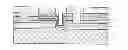
A multilevel resistive memory having a large storage capacity comprises a top electrode and a bottom electrode, and a combination of a plurality of defective layers and switching layers interposed therebetween. As shown in FIG. 1, the top electrode and the bottom electrode are metal films (for example, W, Al, Pt, TIN, etc.), the top electrode and the bottom electrode are respectively contacted with a switching material layer (a film such as Ta2O5, TiO2, HfO2, etc.), and the defective layers (metal film such as Ti, Au, Ag, etc.) are interposed between the switching material layers.
An embodiment of the present invention further provides a method for fabricating the above multilevel resistive memory. By taking a memory cell having two switching material layers and one defective layer between the top electrode and the bottom electrode as an example, the processing method comprises the following steps:
1) depositing a metal layer with a thickness between 150 nm and 500 nm over a substrate (generally may be a silicon substrate, and also may be a glass substrate, etc.), and performing a photolithographic process on the metal layer to form a bottom electrode pattern;
2) depositing a switching material film with a thickness between 10 nm and 80 nm;
3) depositing a defective layer with a thickness between 2 nm and 50 nm;
4) depositing a switching material film with a thickness between 10 nm and 80 nm again;
5) depositing a defective layer with a thickness between 2 nm and 50 nm again;
6) depositing a switching material film with a thickness between 10nm and 80nm; and
7) depositing a metal layer for the top electrode with a thickness between 150 nm and 500 nm, and performing a photolithography on the metal layer to form a top electrode pattern.
An operating principle of a memory according to an embodiment of the present invention is described as follow.
In initial state, the entire memory cell is not turned-on, that is, in the high resistance state, and the resistance is noted as R0. When a suitable bias voltage is applied to the top electrode, oxygen vacancies are generated in the switching material layer, and accumulate from the top electrode toward the bottom electrode, and thus to form an increasingly grown conductive filament. When the conductive filament contacts with the first layer of defective layers, the switching material layer between the top electrode and the first layer of defective layers becomes into the low resistance state, and the entire memory cell has a correspondingly decreased resistance which is noted as R1. When the bias voltage is continually applied, the conductive filament continues to grow, and as the conductive filament contacts with the second layer of defective layers, the switching material layer between the top electrode and the second layer of defective layers becomes into the low resistance state, and the entire memory cell has a further decreased resistance which is noted as R2. Similarly, when the bias voltage is continually applied, the conductive filament grows to the bottom electrode, and the switching material layers in the entire structure are all turned-on, having a minimum resistance noted as R3 at this time. As such, the memory cell may store four levels (R0, R1, R2, and R3).
If more defective layers are interposed between the intermediate switching layers, the operating principle of the memory is the same as above. As for a resistive memory cell with multilevel storage characteristic, if a structure of an embodiment of the present invention is used, the data which can be stored could be increased.
BRIEF DESCRIPTION OF THE DRAWINGS
FIG. 1 is a schematic structural diagram of a resistive memory according to an embodiment of the present invention; and
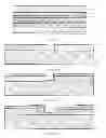
FIG. 2 are diagrams showing a process flow of an embodiment of the present invention.
In the drawings, 1—an top electrode, 2—a switching material layer, 3—a defective layer, 4—a bottom electrode, and 5—a substrate.
DETAILED DESCRIPTION OF THE EMBODIMENTS
The present invention will now be further described in detail by a specific embodiment in conjunction with drawings.
A method for fabricating a resistive memory according to an embodiment of the present invention is described as follow.
1) A silicon substrate is usually selected as a substrate. W is used as a bottom electrode, and the bottom electrode with a thickness of 200 nm is formed by using a physical vapor deposition (PVD) method or other film forming methods used in IC process. The bottom electrode is patterned by a photolithographic process , as shown in FIG. 2(a).
2) Ta2O5 with a thickness of 10 nm is sputtered, as shown in FIG. 2(b).
3) A photolithographic process is performed, and a Ti film with a thickness of 10 nm is formed by using a physical vapor deposition (PVD) method or other film forming methods used in the IC process. The Ti film is lifted off to remain a Ti defective layer in a memory cell region, as shown in FIG. 2(c).
4) Ta2O5 with a thickness of 10 nm is sputtered, as shown in FIG. 2(d).
5) A photolithographic process is performed, and a Ti film with a thickness of 10 nm is formed by using a physical vapor deposition (PVD) method or other film forming methods used in the IC process. The Ti film is lifted off to remain a Ti defective layer in a memory cell region, as shown in FIG. 2(e).
6) Ta2O5 with a thickness of 10 nm is sputtered, as shown in FIG. 2(f).
7) A via for the bottom electrode is defined by a photolithographic process and RIE (reactive ion etch) etching process, as shown in FIG. 2(g).
8) A photolithographic process is performed to fabricate an top electrode. A TiN film with a thickness between 150 nm and 500 nm is formed by using a physical vapor deposition (PVD) method or other film forming methods used in the IC process. The top electrode pattern is defined by a lift-off process and the bottom electrode contact is defined, as shown in FIG. 2(h).
Finally, it is to be noted that, the above embodiments are only used for illustrating technical solutions of the present invention, and do not limit the present invention. While the present invention has been described with respect to preferable embodiments, it will be understood by one skilled in the art that various modifications and substitutions can be made without departing from the spirit or scope of the technical solutions of the present invention.
Claims
What is claimed is:1. A multilevel resistive memory having large storage capacity comprising an top electrode and a bottom electrode, wherein a combination of a plurality of switching layers and defective layers is interposed between the top electrode and the bottom electrode, wherein, the top electrode and the bottom electrode are respectively contacted with a switching layer, and the defective layers are interposed between the switching layers.
2. The multilevel resistive memory having large storage capacity according to claim 1, wherein the top electrode and the bottom electrode are W, Al, Pt or TiN metal films with a thickness between 150 nm and 500 nm.
3. The multilevel resistive memory having large storage capacity according to claim 1, wherein the switching layers are Ta2O5, TiO2 or HfO2 films with a thickness between 10 nm and 80 nm.
4. The multilevel resistive memory having large storage capacity according to claim 1, wherein the defective layers are Ti, Au or Ag metal films with a thickness between 2 nm and 50 nm.
Images & Drawings included:

Sources:
- United States Patent and Trademark Office - verify current appl. status at the USPTO↗
Recent applications in this class:
- » 20130343115 2013-12-26
Resistance memory cell and operation method thereof - » 20130329483 2013-12-12
Filamentary memory devices and methods - » 20130299763 2013-11-14
Variable resistance memory device and method for fabricating the same - » 20130248806 2013-09-26
VARIABLE RESISTANCE MEMORY DEVICE AND METHOD FOR FABRICATING THE SAME - » 20130228735 2013-09-05
Interfacial oxide used as switching layer in a nonvolatile resistive memory element - » 20130214237 2013-08-22
Nonvolatile memory device using a tunnel oxide layer and oxygen blocking layer as a current limiter element - » 20130214236 2013-08-22
Using TiON as electrodes and switching layers in ReRAM devices - » 20130210193 2013-08-15
ReRAM stacks preparation by using single ALD or PVD chamber - » 20130200324 2013-08-08
Transition metal oxide bilayers - » 20130193394 2013-08-01
Incorporation of oxygen into memory cells
Recent applications for this Assignee:
- » 20250224316 2025-07-10
FROZEN SOLUTION SAMPLE PREPARATION DEVICE APPLICABLE TO ULTRA-HIGH VACUUM SYSTEM - » 20250195542 2025-06-19
METABOLIC DISEASE THERAPEUTIC AGENT OR PREVENTIVE AGENT - » 20250194970 2025-06-19
DIABETES BIOSENSOR - » 20250104769 2025-03-27
COMPLEMENTARY PHOTOTRANSISTOR PIXEL UNIT, SENSING AND COMPUTING ARRAY STRUCTURE AND OPERATION METHOD THEREOF - » 20250082746 2025-03-13
CIRCULAR RNA VACCINES AGAINST SARS-COV-2 VARIANTS AND METHODS OF USE THEREOF - » 20250081574 2025-03-06
METHOD FOR IMPROVING SHORT-CIRCUIT CAPABILITY OF ENHANCEMENT-MODE GaN HEMT AND ITS DEVICE STRUCTURE - » 20250060650 2025-02-20
NONLINEAR OPTICAL CRYSTAL STRUCTURE - » 20250057450 2025-02-20
Intelligent deformable microneedle and manufacturing method therefor - » 20250041624 2025-02-06
METHOD FOR ENHANCING ACTIVITY OF PHOTOSENSITIZER BY MAGNETIC FIELD - » 20250027936 2025-01-23
IMMUNOASSAY DEVICE, AND PREPARATION METHOD AND USE THEREOF