Methods and arrangements relating to semiconductor packages including multi-memory dies
US20140021598A1
2014-01-23
13/947,936
2013-07-22
✅ Patent granted
US 9,117,790 B2
2015-08-25
-
-
A. Sefer | Dilinh Nguyen
2033-07-22
Abstract:
In an embodiment, there is provided a packaging arrangement comprising a substrate; a multi-memory die coupled to the substrate, wherein the multi-memory die comprises multiple individual memory dies, and each of the multiple individual memory dies is defined as an individual memory die within a wafer of semiconductor material during production of memory dies, and the multi-memory die is created by singulating the wafer of semiconductor material into memory dies, where at least one of the memory dies is the multi-memory die that includes the multiple individual memory dies that are still physically connected together; and a semiconductor die coupled to the multi-memory die and the substrate, wherein the semiconductor die is configured as a system on a chip, wherein at least one of the multi-memory die and the semiconductor die is attached to the substrate.
Assignee:
- MARVELL WORLD TRADE LTD. 1,859 St. Michael, Barbados
Applicant:
Interested in similar patents?
Get notified when new applications in this technology area are published.
Classification:
H01L21/82 » CPC further
Processes or apparatus adapted for the manufacture or treatment of semiconductor or solid state devices or of parts thereof; Manufacture or treatment of devices consisting of a plurality of solid state components formed in or on a common substrate or of parts thereof; Manufacture of integrated circuit devices or of parts thereof; Manufacture or treatment of devices consisting of a plurality of solid state components or integrated circuits formed in, or on, a common substrate with subsequent division of the substrate into plural individual devices to produce devices, e.g. integrated circuits, each consisting of a plurality of components
H01L23/36 » CPC main
Details of semiconductor or other solid state devices; Arrangements for cooling, heating, ventilating or temperature compensation ; Temperature sensing arrangements Selection of materials, or shaping, to facilitate cooling or heating, e.g. heatsinks
H01L24/48 » CPC further
Arrangements for connecting or disconnecting semiconductor or solid-state bodies; Methods or apparatus related thereto; Means for bonding being attached to, or being formed on, the surface to be connected, e.g. chip-to-package, die-attach, "first-level" interconnects; Manufacturing methods related thereto; Wire connectors; Manufacturing methods related thereto; Structure, shape, material or disposition of the wire connectors after the connecting process of an individual wire connector
H01L2224/73207 » CPC further
Indexing scheme for arrangements for connecting or disconnecting semiconductor or solid-state bodies and methods related thereto as covered by; Means for bonding being of different types provided for in two or more of groups; Location after the connecting process on the same surface Bump and wire connectors
H01L25/065 IPC
Assemblies consisting of a plurality of individual semiconductor or other solid state devices ; Multistep manufacturing processes thereof all the devices being of a type provided for in the same subgroup of groups - , e.g. assemblies of rectifier diodes the devices not having separate containers the devices being of a type provided for in group
H01L24/73 » CPC further
Arrangements for connecting or disconnecting semiconductor or solid-state bodies; Methods or apparatus related thereto Means for bonding being of different types provided for in two or more of groups , , , , , , ,
H01L25/0652 » CPC further
Assemblies consisting of a plurality of individual semiconductor or other solid state devices ; Multistep manufacturing processes thereof all the devices being of a type provided for in the same subgroup of groups - , e.g. assemblies of rectifier diodes the devices not having separate containers the devices being of a type provided for in group the devices being arranged next and on each other, i.e. mixed assemblies
H01L25/105 » CPC further
Assemblies consisting of a plurality of individual semiconductor or other solid state devices ; Multistep manufacturing processes thereof all the devices being of a type provided for in the same subgroup of groups - , e.g. assemblies of rectifier diodes the devices having separate containers the devices being of a type provided for in group
H01L24/13 » CPC further
Arrangements for connecting or disconnecting semiconductor or solid-state bodies; Methods or apparatus related thereto; Means for bonding being attached to, or being formed on, the surface to be connected, e.g. chip-to-package, die-attach, "first-level" interconnects; Manufacturing methods related thereto; Bump connectors ; Manufacturing methods related thereto; Structure, shape, material or disposition of the bump connectors prior to the connecting process of an individual bump connector
H01L24/16 » CPC further
Arrangements for connecting or disconnecting semiconductor or solid-state bodies; Methods or apparatus related thereto; Means for bonding being attached to, or being formed on, the surface to be connected, e.g. chip-to-package, die-attach, "first-level" interconnects; Manufacturing methods related thereto; Bump connectors ; Manufacturing methods related thereto; Structure, shape, material or disposition of the bump connectors after the connecting process of an individual bump connector
H01L24/32 » CPC further
Arrangements for connecting or disconnecting semiconductor or solid-state bodies; Methods or apparatus related thereto; Means for bonding being attached to, or being formed on, the surface to be connected, e.g. chip-to-package, die-attach, "first-level" interconnects; Manufacturing methods related thereto; Layer connectors, e.g. plate connectors, solder or adhesive layers; Manufacturing methods related thereto; Structure, shape, material or disposition of the layer connectors after the connecting process of an individual layer connector
H01L2224/0401 » CPC further
Indexing scheme for arrangements for connecting or disconnecting semiconductor or solid-state bodies and methods related thereto as covered by; Means for bonding being attached to, or being formed on, the surface to be connected, e.g. chip-to-package, die-attach, "first-level" interconnects; Manufacturing methods related thereto; Bonding areas; Manufacturing methods related thereto; Structure, shape, material or disposition of the bonding areas prior to the connecting process Bonding areas specifically adapted for bump connectors, e.g. under bump metallisation [UBM]
H01L2224/04042 » CPC further
Indexing scheme for arrangements for connecting or disconnecting semiconductor or solid-state bodies and methods related thereto as covered by; Means for bonding being attached to, or being formed on, the surface to be connected, e.g. chip-to-package, die-attach, "first-level" interconnects; Manufacturing methods related thereto; Bonding areas; Manufacturing methods related thereto; Structure, shape, material or disposition of the bonding areas prior to the connecting process Bonding areas specifically adapted for wire connectors, e.g. wirebond pads
H01L2224/73215 » CPC further
Indexing scheme for arrangements for connecting or disconnecting semiconductor or solid-state bodies and methods related thereto as covered by; Means for bonding being of different types provided for in two or more of groups; Location after the connecting process on the same surface Layer and wire connectors
H01L2224/73253 » CPC further
Indexing scheme for arrangements for connecting or disconnecting semiconductor or solid-state bodies and methods related thereto as covered by; Means for bonding being of different types provided for in two or more of groups; Location after the connecting process on different surfaces Bump and layer connectors
H01L2224/73265 » CPC further
Indexing scheme for arrangements for connecting or disconnecting semiconductor or solid-state bodies and methods related thereto as covered by; Means for bonding being of different types provided for in two or more of groups; Location after the connecting process on different surfaces Layer and wire connectors
H01L2225/0651 » CPC further
Details relating to assemblies covered by the group but not provided for in its subgroups; All the devices being of a type provided for in the same subgroup of groups - the devices not having separate containers the devices being of a type provided for in group; Stacked arrangements of devices Wire or wire-like electrical connections from device to substrate
H01L2225/06506 » CPC further
Details relating to assemblies covered by the group but not provided for in its subgroups; All the devices being of a type provided for in the same subgroup of groups - the devices not having separate containers the devices being of a type provided for in group; Stacked arrangements of devices Wire or wire-like electrical connections between devices
H01L2225/06562 » CPC further
Details relating to assemblies covered by the group but not provided for in its subgroups; All the devices being of a type provided for in the same subgroup of groups - the devices not having separate containers the devices being of a type provided for in group; Stacked arrangements of devices; Geometry of the stack, e.g. form of the devices, geometry to facilitate stacking at least one device in the stack being rotated or offset
H01L2225/06589 » CPC further
Details relating to assemblies covered by the group but not provided for in its subgroups; All the devices being of a type provided for in the same subgroup of groups - the devices not having separate containers the devices being of a type provided for in group; Stacked arrangements of devices Thermal management, e.g. cooling
H01L2225/1023 » CPC further
Details relating to assemblies covered by the group but not provided for in its subgroups; All the devices being of a type provided for in the same subgroup of groups - the devices having separate containers the devices being of a type provided for in group the containers being in a stacked arrangement the lowermost container comprising a device support the support being an insulating substrate
H01L2225/1058 » CPC further
Details relating to assemblies covered by the group but not provided for in its subgroups; All the devices being of a type provided for in the same subgroup of groups - the devices having separate containers the devices being of a type provided for in group the containers being in a stacked arrangement; Details of electrical connections between containers Bump or bump-like electrical connections, e.g. balls, pillars, posts
H01L2924/1434 » CPC further
Indexing scheme for arrangements or methods for connecting or disconnecting semiconductor or solid-state bodies as covered by; Details of semiconductor or other solid state devices to be connected; Device type; Integrated circuits; Digital devices Memory
H01L2924/15311 » CPC further
Indexing scheme for arrangements or methods for connecting or disconnecting semiconductor or solid-state bodies as covered by; Details of package parts other than the semiconductor or other solid state devices to be connected; Die mounting substrate; Connection portion the connection portion being formed only on the surface of the substrate opposite to the die mounting surface being a ball array, e.g. BGA
H01L2924/15331 » CPC further
Indexing scheme for arrangements or methods for connecting or disconnecting semiconductor or solid-state bodies as covered by; Details of package parts other than the semiconductor or other solid state devices to be connected; Die mounting substrate; Connection portion the connection portion being formed on the die mounting surface of the substrate the connection portion being formed both on the die mounting surface of the substrate and outside the die mounting surface of the substrate being a ball array, e.g. BGA
H01L2924/19107 » CPC further
Indexing scheme for arrangements or methods for connecting or disconnecting semiconductor or solid-state bodies as covered by; Details of hybrid assemblies other than the semiconductor or other solid state devices to be connected; Disposition of discrete passive components off-chip wires
H01L23/48 IPC
Details of semiconductor or other solid state devices Arrangements for conducting electric current to or from the solid state body in operation, e.g. leads, terminal arrangements ; Selection of materials therefor
H01L23/52 IPC
Details of semiconductor or other solid state devices Arrangements for conducting electric current within the device in operation from one component to another, i.e. interconnections, e.g. wires, lead frames
H01L29/40 IPC
Semiconductor devices adapted for rectifying, amplifying, oscillating or switching, or capacitors or resistors with at least one potential-jump barrier or surface barrier, e.g. PN junction depletion layer or carrier concentration layer; Details of semiconductor bodies or of electrodes thereof; Multistep manufacturing processes therefor Electrodes ; Multistep manufacturing processes therefor
H01L23/02 IPC
Details of semiconductor or other solid state devices Containers; Seals
H01L23/00 IPC
Details of semiconductor or other solid state devices
H01L24/29 » CPC further
Arrangements for connecting or disconnecting semiconductor or solid-state bodies; Methods or apparatus related thereto; Means for bonding being attached to, or being formed on, the surface to be connected, e.g. chip-to-package, die-attach, "first-level" interconnects; Manufacturing methods related thereto; Layer connectors, e.g. plate connectors, solder or adhesive layers; Manufacturing methods related thereto; Structure, shape, material or disposition of the layer connectors prior to the connecting process of an individual layer connector
H01L25/10 IPC
Assemblies consisting of a plurality of individual semiconductor or other solid state devices ; Multistep manufacturing processes thereof all the devices being of a type provided for in the same subgroup of groups - , e.g. assemblies of rectifier diodes the devices having separate containers
Description
CROSS-REFERENCES TO RELATED APPLICATIONS
The present disclosure claims priority to U.S. Provisional Patent Application No. 61/674,703, filed Jul. 23, 2012, and U.S. Provisional Patent Application No. 61/675,626, filed Jul. 25, 2012, the disclosures of which are hereby incorporated by reference. The present disclosure is related to U.S. patent application Ser. No. 13/532,444, filed Jun. 25, 2012, and U.S. patent application Ser. No. 13/590,949, filed Aug. 21, 2012, the disclosures of which are hereby incorporated by reference.
TECHNICAL FIELD
Embodiments of the present disclosure relate to the field of integrated circuits, and more particularly, to techniques, structures, and configurations for semiconductor chip packaging.
BACKGROUND
The background description provided herein is for the purpose of generally presenting the context of the disclosure. Work of the presently named inventor(s), to the extent the work is described in this background section, as well as aspects of the description that may not otherwise qualify as prior art at the time of filing, are neither expressly nor impliedly admitted as prior art against the present disclosure.
Electronic devices utilize packages made up of semiconductor dies where the semiconductor dies are arranged and configured to perform various functions. For example, in a package, one semiconductor die may be configured as a system on a chip (SOC) while another semiconductor die may be configured as a memory die. The SOC die and the memory die are then interconnected to perform various functions for an electronic device that houses the package. The semiconductor dies in these packages often generate large amounts of heat. Additionally, the semiconductor dies need access to power (VDD) and ground. Thus, in creating and designing such packages, there are many trade-offs including, cost, heat dissipation and access to VDD and ground, as well as interconnectivity among the semiconductor dies within the package.
SUMMARY
In an embodiment, there is provided a packaging arrangement comprising a substrate; a multi-memory die coupled to the substrate, wherein the multi-memory die comprises multiple individual memory dies, and each of the multiple individual memory dies is defined as an individual memory die within a wafer of semiconductor material during production of memory dies, and the multi-memory die is created by singulating the wafer of semiconductor material into memory dies, where at least one of the memory dies is the multi-memory die that includes the multiple individual memory dies that are still physically connected together; and a semiconductor die coupled to the multi-memory die and the substrate, wherein the semiconductor die is configured as a system on a chip, wherein at least one of the multi-memory die and the semiconductor die is attached to the substrate.
In an embodiment, there is also provided a method comprising providing a substrate; coupling a multi-memory die to the substrate, wherein the multi-memory die comprises multiple individual memory dies, each of the multiple individual memory dies is defined as an individual memory die within a wafer of semiconductor material during production of memory dies, and the multi-memory die is created by singulating the wafer of semiconductor material into memory dies, where at least one of the memory dies is the multi-memory die that includes the multiple individual memory dies that are still physically connected together; coupling a semiconductor die to the multi-memory die and the substrate, wherein the semiconductor die is configured as a system on a chip; and attaching at least one of the multi-memory die and the semiconductor die to the substrate.
BRIEF DESCRIPTION OF THE DRAWINGS
Embodiments will be readily understood by the following detailed description in conjunction with the accompanying drawings. Embodiments are illustrated by way of example and not by way of limitation in the figures of the accompanying drawings.
FIG. 1A schematically illustrates a top view of an example of a packaging arrangement including a multi-memory die that comprises two individual memory dies.
FIG. 1B schematically illustrates a cross-sectional view of the packaging arrangement illustrated in FIG. 1A.
FIGS. 1C and 1D schematically illustrate a top view and a cross-sectional view, respectively, of an example of a packaging arrangement including a multi-memory die that comprises two individual memory dies.
FIGS. 2-8 schematically illustrate cross-sectional views of various packaging arrangements including a multi-memory die that comprises two individual memory dies.
FIG. 9 illustrates an example of a method for creating a packaging arrangement that comprises a semiconductor die coupled to a multi-memory die comprising multiple individual memory dies.
DETAILED DESCRIPTION
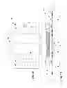
FIG. 1A illustrates a top view of a semiconductor die 102 configured as a system on a chip (SOC) die stacked on a semiconductor die 104 configured as a memory die. The memory die 104 comprises two separate dies 104a, 104b that were not physically separated from each other when the memory die 104 was manufactured. During manufacturing, a wafer (not illustrated) of semiconductor material that has been configured into a plurality of semiconductor dies for production of semiconductor dies is generally singulated or divided, for example, by cutting with a laser, into individual semiconductor dies in order to provide a plurality of individual semiconductor dies that have been physically separated from each other. Thus, a wafer (not illustrated) that was configured with a plurality of memory dies was cut such that the memory die 104 includes the two memory dies 104a, 104b that are still attached to each other. The memory dies 104a, 104b are generally configured as dynamic random access memory (DRAM), although they can be configured as other types of memory if desired.
FIG. 1B schematically illustrates a cross-sectional view of the packaging arrangement illustrated in FIG. 1A. FIG. 1B illustrates the SOC die 102 and the memory die 104 stacked on a substrate 106. The SOC die 102 is attached to the memory die 104 via an appropriate epoxy or glue. Likewise, the memory die 104 is attached to the substrate 106 via an appropriate epoxy or glue. The substrate 106 includes solder balls 108 for attaching the resulting packaging arrangement 100 to another substrate such as, for example, a printed circuit board (PCB), another substrate, etc. (not illustrated). Various bonding pads 110 on the SOC die 102, the memory die 104 and the substrate 106 can be coupled to one another with wire bonds 112 via a wire bonding process. The bonding pads 110 can be configured to be utilized for, for example, signals relating to data, commands and/or addresses, input/output, and access to VDD/ground. Furthermore, wire bonds 112 can be utilized between the SOC die 102 and the substrate 106, and between the memory die 104 and the substrate 106. For example, wire bonds 112 can be utilized to provide access to VDD/ground for the SOC die 102. The packaging arrangement 100 illustrated in FIG. 1B generally provides a reasonable cost but generally does not provide better than average heat dissipation for the SOC die 102 and the memory die 104. Additionally, the packaging arrangement 100 illustrated in FIG. 1A generally provides only minimal VDD/ground access.
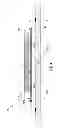
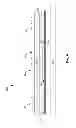
In FIGS. 1A and 1B, the bonding pads 110 of the memory die 104a are disposed on or near to a center section of the memory die 104a, and the bonding pads 110 of the memory die 104b are disposed on or near to a center section of the memory die 104b. However, in an embodiment, the bonding pads 110 of each of the memory dies 104a and 104b can be disposed, for example, near an edge of the corresponding memory die. For example, FIGS. 1C and 1D schematically illustrate a top view and a cross-sectional view, respectively, of an example of a packaging arrangement including a multi-memory die that comprises two individual memory dies. FIGS. 1C and 1D are to an extent similar to FIGS. 1A and 1B, respectively. However, unlike FIGS. 1A and 1B, in FIGS. 1C and 1D, the bonding pads 110 of the memory die 104a are disposed near an edge of the memory die 104a, and the bonding pads 110 of the memory die 104b are disposed near an edge of the memory die 104b. Having the bonding pads 110 disposed near the edges of the memory dies, for example, allows a relatively larger space for the SOC die 102 and consequently, a larger sized SOC die 102 can be used.
In an embodiment, the memory die 104a is a mirror image of the memory die 104b (e.g., the memory die 104a has components and bonding pad connections that are a mirror image those of the memory die 104b). In another embodiment, the memory die 104a is similar or identical to the memory die 104b (e.g., the memory die 104a has components and bonding pad connections that are similar or identical to those of the memory die 104b, and the memory die 104a is a rotation image of the memory die 104b in the figures). In yet another embodiment, the memory die 104a is different from the memory die 104b (e.g., the memory die 104a has components and bonding pad connections that are different from those of the memory die 104b). In an embodiment, the memory dies 104a and 104b form a dual channel memory. In an example, the memory dies 104a and 104b form a dual channel DRAM.
FIG. 2A illustrates a packaging arrangement 200a where a hole 214 is defined within a substrate 106. The packaging arrangement 200 includes an SOC die 102 and a memory die 104 that includes two attached memory dies 104a, 104b, as previously described. As can be seen, wire bonds 112 are utilized to provide various connections between the SOC die 102, the memory die 104 and/or the substrate 106. A heat sink 216 is provided and attached to the memory die 104. The heat sink 216 is attached to the memory die 104 via an appropriate epoxy or glue. Solder balls 108 are provided on the substrate 106 so that the packaging arrangement 200 can be attached to another substrate such as, for example, a PCB, another substrate, etc. (not illustrated). The SOC die 102 is attached to the memory die 104 via an appropriate epoxy or glue. As can be seen, when the memory die 104 is attached to the substrate 106 (via an appropriate epoxy or glue), the SOC die 102 extends into the hole 214. The packaging arrangement 200a illustrated in FIG. 2A generally provides good cost benefits, good heat dissipation for the SOC die 102 and very good heat dissipation for the memory die 104 due to the location of the heat sink 216 adjacent to the memory die 104. Additionally, the packaging arrangement 200a provides for improved VDD/ground access.
FIG. 2B illustrates a packaging arrangement 200b that is similar to the packaging arrangement 200a illustrated in FIG. 2A. In the packaging arrangement 200b, solder balls 218 are provided on the SOC die 102 to provide access to VDD and ground. The packaging arrangement 200b also provides good benefits with respect to cost and heat dissipation for the SOC die 102 and the memory die 104. Additionally, connectivity to VDD and ground is improved by the presence of the solder balls 218 on the SOC die 102 to thereby provide access to VDD and ground when the packaging arrangement 200b is flip chipped onto a substrate such as, for example, a PCB, another substrate, etc. (not illustrated)
FIG. 3 illustrates a packaging arrangement 300 that is similar to the packaging arrangement 100 illustrated in FIG. 1B. In the packaging arrangement 300, a redistribution layer (RDL) 320 is disposed on the memory die 104. An SOC die 102 is placed on the RDL 320 and is attached to the RDL 320 via an appropriate epoxy or glue. Wire bonds 112 between the SOC die 102 and the RDL 320, as well as wire bonds 112 between the RDL 320 and the substrate 106, allow for routing of various signals such as, for example, data, commands/addresses, and access to VDD and ground. Solder balls 108 are included on the substrate 106 for attaching the packaging arrangement 300 to another substrate such as, for example, a PCB, another substrate, etc. (not illustrated). The packaging arrangement 300 of FIG. 3 has increased costs due to the inclusion of the RDL 320 and provides adequate heat dissipation for the SOC die 102 and the memory die 104, as well as adequate access to VDD and ground via the RDL 320.
FIG. 4 illustrates a packaging arrangement 400 similar to the packaging arrangement 300 illustrated in FIG. 3. The SOC die 102 however is attached to the RDL 320 via solder balls 418, which thereby provide direct signal access between the SOC die 102 and the RDL 320. As can be seen, the SOC die 102 in the embodiments of both FIGS. 3 and 4 can be larger and can be almost square in comparison to the SOC die 102 that is illustrated in FIG. 1. This is allowable due to the presence of the RDL 320 as opposed to utilizing the bond pads on the memory die 104. A heat sink 416 is also provided in the packaging arrangement 400 and is attached to the SOC die 102 via an appropriate epoxy or glue. Solder balls 108 are provided on the substrate 106 for attaching the packaging arrangement 400 to another substrate such as, for example, a PCB, another substrate, etc. (not illustrated). The packaging arrangement 400 has increased costs and provides improved heat dissipation for the SOC die 102 as well as for the memory die 104 due to the presence of the heat sink 416. Improved access to VDD and ground is provided via the RDL 320.
FIG. 5 illustrates a packaging arrangement 500 that is configured as a package on package (POP) arrangement. A memory die 104 that includes two attached memory dies 104a, 104b as previously described is attached to a first substrate 106a. The memory die 104 is attached to the substrate 106a via an appropriate epoxy or glue. Holes 514a, 514b are defined within the substrate 106a to allow for wire bonds 112 from the memory die 104 to the substrate 106a. A second substrate 106b is provided that includes the SOC die 102 disposed on the substrate 106b. The SOC die 102 is flip chip attached to the second substrate 106b and thus, the SOC die 102 is attached to the second substrate 106b via solder balls 518 to thereby provide direct signal connectivity between the SOC die 102 and the substrate 106b. The first substrate 106a with the memory die 104 attached thereto is attached to the second substrate 106b via solder balls 108a. Solder balls 108b are provided on the second substrate 106b to attach the POP packaging arrangement 500 to another substrate such as, for example, a PCB, another substrate, etc. (not illustrated). The packaging arrangement 500 generally has average costs associated therewith and provides a fair amount of heat dissipation for the SOC die 102 and the memory die 104. The access to VDD and ground for the SOC die 102 is very good due to the solder ball connection between the SOC die 102 and the second substrate 106b.
FIG. 6 illustrates a packaging arrangement 600 wherein a memory die 104 is attached to a heat sink 616. The memory die 104 is attached to the heat sink 616 via an appropriate epoxy or glue. The memory die 104 includes an RDL 320 disposed thereon. An SOC die 102 is flip chip attached via solder balls 618 to the RDL 320 on the memory die 104. Thus, the SOC die 102 has direct signal access to the RDL 320 via the solder balls 618 attaching the SOC die 102 to the RDL 320. The SOC die 102 is also attached to a substrate 106 via an appropriate epoxy or glue. Solder balls 622 are provided between the substrate 106 and the RDL 320 such that when the substrate 106 and SOC die 102 are flip chip attached to the RDL 320 on the memory die 104, direct signal access can be provided between the substrate 106 and the RDL 320. Solder balls 108 are provided on the substrate 106 to attach the packaging arrangement 600 to another substrate such as, for example, a PCB, another substrate, etc. (not illustrated). The packaging arrangement 600 provides improved cost and very good heat dissipation, due to the heat sink 616, for the SOC die 102 and the memory die 104. Additionally, access to the VDD and ground is also very good due to the RDL 320.
FIG. 7 illustrates a packaging arrangement 700 in which an SOC die 102 is attached to a heat sink 716. The SOC die 102 can be attached to the heat sink 716 via an appropriate epoxy or glue. A memory die 104 is attached to a substrate 106. The memory die 104 can be attached to the substrate 106 via an appropriate epoxy or glue. Holes 714a, 714b are defined within the substrate 106 so that wire bonds 112 can be utilized to couple the memory die 104 to the substrate 106 by routing the wire bonds 112 through the holes 714a, 714b within the substrate 106. The SOC die 102 can be flip chip attached to the substrate 106 and thus, solder balls 718 provide direct signal access between the substrate 106 and the SOC die 102. Solder balls 108 are provided on the substrate 106 so that the packaging arrangement 700 can be attached to another substrate such as, for example, a PCB, another substrate, etc. (not illustrated). The packaging arrangement 700 provides adequate cost and very good heat dissipation for the SOC die 102 as well as the memory die 104 due to the heat sink 716. Access to VDD and ground is generally adequate.
FIG. 8 illustrates a packaging arrangement 800 that is similar to the packaging arrangement 700 of FIG. 7. In the packaging arrangement 800 of FIG. 8, the SOC die 102 is wider than the SOC die 102 in the packaging arrangement 700 of FIG. 7. Thus, when the SOC die 102 with the heat sink 716 attached thereto is flip chip attached to the substrate 106, the SOC die 102 can be attached to the substrate 106 beyond the holes 714a, 714b defined within the substrate 106. The packaging arrangement 800 provides adequate cost for the packaging arrangement 800 and very good heat dissipation for the SOC die 102 as well as the memory die 104 due to the heat sink 716. Access to VDD and ground is generally adequate.
While the various packaging arrangements have been described and illustrated utilizing a memory die 104 that includes two memory dies 104a, 104b that are still attached to each other, it is to be noted that memory dies can be utilized that include only a single memory die. In such embodiments, the memory die will generally be narrower than the memory die 104 described and illustrated in FIGS. 1-8. Also, memory dies can be used that include more than two memory dies 104a, 104b that are still attached to each other. In such embodiments, the memory die will generally be wider and/or longer than the memory die 104 described and illustrated in FIGS. 1-8. The multi-memory dies 104 can include arrangements of individual memory dies 104a, 104b of one by two, two by two, two by three, etc. These examples are not meant to be limiting.
FIG. 9 illustrates an example of a method 900 for creating a packaging arrangement, such as, for example, the packaging arrangements of FIGS. 1-8. At 902, a substrate is provided. At 904, a multi-memory die is coupled to the substrate. Each of the multiple individual memory dies is defined as an individual memory die within a wafer of semiconductor material during production of memory dies. The multi-memory die is created by singulating the wafer of semiconductor material into memory dies, where at least one of the memory dies is the multi-memory die that includes the multiple individual memory dies that are still physically connected together. At 906, a semiconductor die is coupled to the multi-memory die and the substrate. The semiconductor die is configured as a system on a chip. At 908, at least one of the multi-memory die and the semiconductor die is attached to the substrate.
Various operations may have been described as multiple discrete actions or operations in turn, in a manner that is most helpful in understanding the claimed subject matter. However, the order of description should not be construed as to imply that these operations are necessarily order dependent. In particular, these operations may not be performed in the order of presentation. Operations described may be performed in a different order than the described embodiment. Various additional operations may be performed and/or described operations may be omitted in additional embodiments.
The description may use the terms “embodiment” or “embodiments,” which may each refer to one or more of the same or different embodiments. Furthermore, the terms “comprising,” “including,” “having,” and the like, as used with respect to embodiments, are synonymous.
Although certain embodiments have been illustrated and described herein, it will be appreciated by those of ordinary skill in the art that a wide variety of alternate and/or equivalent embodiments or implementations calculated to achieve the same purposes may be substituted for the embodiments illustrated and described without departing from the scope. Those with skill in the art will readily appreciate that embodiments may be implemented in a very wide variety of ways. This application is intended to cover any adaptations or variations of the embodiments discussed herein. Therefore, it is manifestly intended that embodiments be limited only by the claims and the equivalents thereof.
Claims
What is claimed is:1. A packaging arrangement comprising:
a substrate;
a multi-memory die coupled to the substrate, wherein the multi-memory die comprises multiple individual memory dies and
each of the multiple individual memory dies is defined as an individual memory die within a wafer of semiconductor material during production of memory dies, and
the multi-memory die is created by singulating the wafer of semiconductor material into memory dies, where at least one of the memory dies is the multi-memory die that includes the multiple individual memory dies that are still physically connected together; and
a semiconductor die coupled to the multi-memory die and the substrate, wherein the semiconductor die is configured as a system on a chip,
wherein at least one of the multi-memory die and the semiconductor die is attached to the substrate.
2. The packaging arrangement of claim 1, wherein both the multi-memory die and the semiconductor die are attached to the substrate.
3. The packaging arrangement of claim 2, wherein the semiconductor die is attached to the substrate via a flip chip process.
4. The packaging arrangement of claim 1, wherein the semiconductor die is coupled to the substrate via a wire bonding process.
5. The packaging arrangement of claim 1, further comprising a redistribution layer attached to the multi-memory die.
6. The packaging arrangement of claim 5, wherein the semiconductor die is coupled to the redistribution layer, and thereby the multi-memory die, via a flip chip process.
7. The packaging arrangement of claim 5, wherein the semiconductor die is coupled to the redistribution layer, and thereby the multi-memory die, via a wire bonding process.
8. The packaging arrangement of claim 1, further comprising a heat sink attached to one of the semiconductor die or the multi-memory die.
9. The packaging arrangement of claim 1, wherein the multi-memory die is attached to the substrate via an epoxy or glue.
10. The packaging arrangement of claim 1, wherein the semiconductor die is attached to the substrate via an epoxy or glue.
11. The packaging arrangement of claim 1, wherein the semiconductor die is attached to the multi-memory die via an epoxy or glue.
12. The packaging arrangement of claim 1, wherein the substrate has a hole defined therein and the multi-memory die is coupled to the substrate via a wire bonding process through the hole.
13. The packaging arrangement of claim 12, wherein the multi-memory die is coupled to the semiconductor die via a wire bonding process through the hole.
14. The packaging arrangement of claim 12, wherein:
the substrate is a first substrate;
the packaging arrangement further comprises a second substrate;
the second substrate is coupled to the first substrate via solder balls; and
the semiconductor die is coupled to the second substrate, and thereby the first substrate and the multi-memory die, via a flip-chip process.
15. A method comprising:
providing a substrate;
coupling a multi-memory die to the substrate, wherein
the multi-memory die comprises multiple individual memory dies,
each of the multiple individual memory dies is defined as an individual memory die within a wafer of semiconductor material during production of memory dies, and
the multi-memory die is created by singulating the wafer of semiconductor material into memory dies, where at least one of the memory dies is the multi-memory die that includes the multiple individual memory dies that are still physically connected together;
coupling a semiconductor die to the multi-memory die and the substrate, wherein the semiconductor die is configured as a system on a chip; and
attaching at least one of the multi-memory die and the semiconductor die to the substrate.
16. The method of claim 15, wherein the multi-memory die is coupled to the substrate via one of a flip chip process or a wire bonding process.
17. The method of claim 15, wherein the semiconductor die is coupled to the multi-memory die via one of a flip chip process or a wire bonding process.
18. The method of claim 15, wherein the multi-memory die is coupled to the substrate via one of a flip chip process or a wire bonding process.
19. The method of claim 15, wherein the multi-memory die is attached to the substrate via an epoxy or glue.
20. The method of claim 15, wherein the semiconductor die is attached to the substrate via an epoxy or glue.
Images & Drawings included:


Sources:
- United States Patent and Trademark Office - verify current appl. status at the USPTO↗
Similar patent applications:
Recent applications in this class:
- » 20250293110 2025-09-18
SEMICONDUCTOR MODULE AND POWER CONVERSION UNIT - » 20250259906 2025-08-14
THERMAL PERFORMANCE IN HYBRID BONDED 3D DIE STACKS - » 20250226278 2025-07-10
SEMICONDUCTOR STRUCTURE AND MANUFACTURING METHOD THEREOF - » 20250226277 2025-07-10
SEMICONDUCTOR DEVICE AND MANUFACTURING METHOD THEREOF - » 20250210440 2025-06-26
SEMICONDUCTOR PACKAGE AND MANUFACTURING METHOD FOR THE SAME - » 20250201648 2025-06-19
INTEGRATED CIRCUIT PACKAGES - » 20250201647 2025-06-19
PACKAGE STRUCTURE - » 20250118615 2025-04-10
PACKAGE STRUCTURE INCLUDING A HEAT DISSIPATION STRUCTURE AND METHODS OF FORMING THE SAME - » 20250112105 2025-04-03
SEMICONDUCTOR ASSEMBLIES INCLUDING VERTICALLY INTEGRATED CIRCUITS AND METHODS OF MANUFACTURING THE SAME - » 20250105082 2025-03-27
PACKAGING STRUCTURE AND METHOD FOR FORMING THE SAME
Recent applications for this Assignee:
- » 20200382996 2020-12-03
Methods and apparatus for distributing baseband signal processing of fifth (5G) new radio uplink signals - » 20200202894 2020-06-25
Differential interface transmission of fly-height control data - » 20200202893 2020-06-25
Zone self servo writing with synchronized parallel clocks - » 20200186342 2020-06-11
Self-encryption drive (SED) - » 20200186340 2020-06-11
Self-encryption drive (SED) - » 20200184998 2020-06-11
Reducing offset of a differential signal output by a capacitive coupling stage of a hard disk drive preamplifier - » 20200135233 2020-04-30
Thermal compensation for laser in heat assisted magnetic recording - » 20200133898 2020-04-30
Artificial intelligence-enabled management of storage media access - » 20200066706 2020-02-27
Sub-device field-effect transistor architecture for integrated circuits - » 20200066299 2020-02-27
Pulse-based writing for magnetic storage media