Bump structure and method of forming same
US20140077358A1
2014-03-20
13/712,722
2012-12-12
✅ Patent granted
US 9,111,817 B2
2015-08-18
-
-
Bilkis Jahan | Kevin Quinto
Slater & Matsil, L.L.P.
2033-02-06
Abstract:
An embodiment bump on trace (BOT) structure includes a contact element supported by an integrated circuit, an under bump metallurgy (UBM) feature electrically coupled to the contact element, a metal bump on the under bump metallurgy feature, and a substrate trace on a substrate, the substrate trace coupled to the metal bump through a solder joint and intermetallic compounds, a ratio of a first cross sectional area of the intermetallic compounds to a second cross sectional area of the solder joint greater than forty percent.
Inventors:
- Tin-Hao Kuo 59 🇹🇼 Hsin-Chu, Taiwan
- Chen-Shien Chen 319 🇹🇼 Zhubei City, Taiwan
- Yu-Wei Lin 36 🇹🇼 New Taipei City, Taiwan
- Taiwan Semiconductor Manufacturing Company, Ltd. 263 🇺🇸 , United States
- Yu-Jen Tseng 14 🇹🇼 Hsin-Chu, Taiwan
- Guan-Yu Chen 9 🇹🇼 Hsin-Chu, Taiwan
- Chen-Shien Chen 311 🇹🇼 Zhubei, Taiwan
- Yu-Wei Lin 29 🇹🇼 New Taipei, Taiwan
Assignee:
- TAIWAN SEMICONDUCTOR MANUFACTURING COMPANY, LTD. 8,890 🇹🇼 Hsin-Chu, Taiwan
Applicant:
Interested in similar patents?
Get notified when new applications in this technology area are published.
Classification:
H01L24/13 » CPC main
Arrangements for connecting or disconnecting semiconductor or solid-state bodies; Methods or apparatus related thereto; Means for bonding being attached to, or being formed on, the surface to be connected, e.g. chip-to-package, die-attach, "first-level" interconnects; Manufacturing methods related thereto; Bump connectors ; Manufacturing methods related thereto; Structure, shape, material or disposition of the bump connectors prior to the connecting process of an individual bump connector
H01L24/11 » CPC further
Arrangements for connecting or disconnecting semiconductor or solid-state bodies; Methods or apparatus related thereto; Means for bonding being attached to, or being formed on, the surface to be connected, e.g. chip-to-package, die-attach, "first-level" interconnects; Manufacturing methods related thereto; Bump connectors ; Manufacturing methods related thereto Manufacturing methods
H01L23/00 IPC
Details of semiconductor or other solid state devices
H01L21/76885 » CPC further
Processes or apparatus adapted for the manufacture or treatment of semiconductor or solid state devices or of parts thereof; Manufacture or treatment of devices consisting of a plurality of solid state components formed in or on a common substrate or of parts thereof; Manufacture of integrated circuit devices or of parts thereof; Manufacture of specific parts of devices defined in group; Applying interconnections to be used for carrying current between separate components within a device comprising conductors and dielectrics characterised by the formation and the after-treatment of the conductors By forming conductive members before deposition of protective insulating material, e.g. pillars, studs
H01L24/16 » CPC further
Arrangements for connecting or disconnecting semiconductor or solid-state bodies; Methods or apparatus related thereto; Means for bonding being attached to, or being formed on, the surface to be connected, e.g. chip-to-package, die-attach, "first-level" interconnects; Manufacturing methods related thereto; Bump connectors ; Manufacturing methods related thereto; Structure, shape, material or disposition of the bump connectors after the connecting process of an individual bump connector
H01L21/4853 » CPC further
Processes or apparatus adapted for the manufacture or treatment of semiconductor or solid state devices or of parts thereof; Manufacture or treatment of semiconductor devices or of parts thereof the devices having at least one potential-jump barrier or surface barrier, e.g. PN junction, depletion layer or carrier concentration layer; Manufacture or treatment of parts, e.g. containers, prior to assembly of the devices, using processes not provided for in a single one of the subgroups -; Conductive parts; Leads on or in insulating or insulated substrates, e.g. metallisation Connection or disconnection of other leads to or from a metallisation, e.g. pins, wires, bumps
H01L23/49811 » CPC further
Details of semiconductor or other solid state devices; Arrangements for conducting electric current to or from the solid state body in operation, e.g. leads, terminal arrangements ; Selection of materials therefor consisting of soldered constructions; Leads, on insulating substrates, Additional leads joined to the metallisation on the insulating substrate, e.g. pins, bumps, wires, flat leads
H01L24/14 » CPC further
Arrangements for connecting or disconnecting semiconductor or solid-state bodies; Methods or apparatus related thereto; Means for bonding being attached to, or being formed on, the surface to be connected, e.g. chip-to-package, die-attach, "first-level" interconnects; Manufacturing methods related thereto; Bump connectors ; Manufacturing methods related thereto; Structure, shape, material or disposition of the bump connectors prior to the connecting process of a plurality of bump connectors
H01L24/81 » CPC further
Arrangements for connecting or disconnecting semiconductor or solid-state bodies; Methods or apparatus related thereto; Methods for connecting semiconductor or other solid state bodies using means for bonding being attached to, or being formed on, the surface to be connected using a bump connector
H01L2224/11472 » CPC further
Indexing scheme for arrangements for connecting or disconnecting semiconductor or solid-state bodies and methods related thereto as covered by; Means for bonding being attached to, or being formed on, the surface to be connected, e.g. chip-to-package, die-attach, "first-level" interconnects; Manufacturing methods related thereto; Bump connectors; Manufacturing methods related thereto; Manufacturing methods using a lift-off mask Profile of the lift-off mask
H01L2224/1357 » CPC further
Indexing scheme for arrangements for connecting or disconnecting semiconductor or solid-state bodies and methods related thereto as covered by; Means for bonding being attached to, or being formed on, the surface to be connected, e.g. chip-to-package, die-attach, "first-level" interconnects; Manufacturing methods related thereto; Bump connectors; Manufacturing methods related thereto; Structure, shape, material or disposition of the bump connectors prior to the connecting process of an individual bump connector; Coating Single coating layer
H01L2224/14051 » CPC further
Indexing scheme for arrangements for connecting or disconnecting semiconductor or solid-state bodies and methods related thereto as covered by; Means for bonding being attached to, or being formed on, the surface to be connected, e.g. chip-to-package, die-attach, "first-level" interconnects; Manufacturing methods related thereto; Bump connectors; Manufacturing methods related thereto; Structure, shape, material or disposition of the bump connectors prior to the connecting process of a plurality of bump connectors; Shape Bump connectors having different shapes
H01L2224/8181 » CPC further
Indexing scheme for arrangements for connecting or disconnecting semiconductor or solid-state bodies and methods related thereto as covered by; Methods for connecting semiconductor or other solid state bodies using means for bonding being attached to, or being formed on, the surface to be connected using a bump connector; Bonding techniques; Soldering or alloying involving forming an intermetallic compound at the bonding interface
H01L2224/81191 » CPC further
Indexing scheme for arrangements for connecting or disconnecting semiconductor or solid-state bodies and methods related thereto as covered by; Methods for connecting semiconductor or other solid state bodies using means for bonding being attached to, or being formed on, the surface to be connected using a bump connector; Arrangement of the bump connectors prior to mounting wherein the bump connectors are disposed only on the semiconductor or solid-state body
Y10T29/49144 » CPC further
Metal working; Method of mechanical manufacture; Electrical device making; Conductor or circuit manufacturing; On flat or curved insulated base, e.g., printed circuit, etc.; Assembling to base an electrical component, e.g., capacitor, etc. by metal fusion
H01L23/48 IPC
Details of semiconductor or other solid state devices Arrangements for conducting electric current to or from the solid state body in operation, e.g. leads, terminal arrangements ; Selection of materials therefor
H01L21/768 IPC
Processes or apparatus adapted for the manufacture or treatment of semiconductor or solid state devices or of parts thereof; Manufacture or treatment of devices consisting of a plurality of solid state components formed in or on a common substrate or of parts thereof; Manufacture of integrated circuit devices or of parts thereof; Manufacture of specific parts of devices defined in group Applying interconnections to be used for carrying current between separate components within a device comprising conductors and dielectrics
H01L21/48 IPC
Processes or apparatus adapted for the manufacture or treatment of semiconductor or solid state devices or of parts thereof; Manufacture or treatment of semiconductor devices or of parts thereof the devices having at least one potential-jump barrier or surface barrier, e.g. PN junction, depletion layer or carrier concentration layer Manufacture or treatment of parts, e.g. containers, prior to assembly of the devices, using processes not provided for in a single one of the subgroups -
H01L23/498 IPC
Details of semiconductor or other solid state devices; Arrangements for conducting electric current to or from the solid state body in operation, e.g. leads, terminal arrangements ; Selection of materials therefor consisting of soldered constructions Leads, on insulating substrates,
H01L2224/11462 » CPC further
Indexing scheme for arrangements for connecting or disconnecting semiconductor or solid-state bodies and methods related thereto as covered by; Means for bonding being attached to, or being formed on, the surface to be connected, e.g. chip-to-package, die-attach, "first-level" interconnects; Manufacturing methods related thereto; Bump connectors; Manufacturing methods related thereto; Manufacturing methods by blanket deposition of the material of the bump connector; Plating Electroplating
Description
CROSS-REFERENCE TO RELATED APPLICATIONS
This application claims the benefit of U.S. Provisional Application No. 61/707,442, filed on Sep. 28, 2012, entitled “Bump Structure and Method of Forming Same,” of U.S. Provisional Application No. 61/707,609, filed on Sep. 28, 2012, entitled “Interconnection Structure Method of Forming Same,” of U.S. Provisional Application No. 61/707,644, filed on Sep. 28, 2012, entitled “Metal Bump and Method of Manufacturing Same,” and of U.S. Provisional Application No. 61/702,624, filed on Sep. 18, 2012, entitled “Ladd Bump Structures and Methods of Making the Same,” which applications are hereby incorporated herein by reference.
BACKGROUND
In the trend of smaller package and higher input/output (I/O) counts, a finer pitch is needed for a flip-chip bump on trace (BOT) package. The finer pitch requirement causes bump dimensions to shrink. As such, the area of metal/solder interface (metal bump) and solder/trace joint interface also decreases. So, electromigration (EM) resistance at both “bump-to-trace” and “trace-to-bump” sites get worse due to higher current density.
BRIEF DESCRIPTION OF THE DRAWINGS
For a more complete understanding of the present disclosure, and the advantages thereof, reference is now made to the following descriptions taken in conjunction with the accompanying drawings, in which:
FIG. 1 is a cross sectional view of an embodiment bump on trace (BOT) structure;
FIG. 2 is a cross sectional view of a metal bump suitable for use with the BOT structure of FIG. 1;
FIG. 3 is a cross sectional view of a metal bump suitable for use with the BOT structure of FIG. 1;
FIG. 4 is a plan view of the metal bump from the BOT structure of FIG. 1 illustrating various periphery shapes; and
FIG. 5 is a method of forming the BOT structure of FIG. 1.
Corresponding numerals and symbols in the different figures generally refer to corresponding parts unless otherwise indicated. The figures are drawn to clearly illustrate the relevant aspects of the embodiments and are not necessarily drawn to scale.
DETAILED DESCRIPTION OF ILLUSTRATIVE EMBODIMENTS
The making and using of the presently preferred embodiments are discussed in detail below. It should be appreciated, however, that the present disclosure provides many applicable inventive concepts that can be embodied in a wide variety of specific contexts. The specific embodiments discussed are merely illustrative and do not limit the scope of the disclosure.
The present disclosure will be described with respect to preferred embodiments in a specific context, namely a bump structure for a bump on trace (BOT) assembly. The concepts in the disclosure may also apply, however, to other semiconductor structures or circuits.
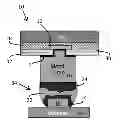
Referring now to FIG. 1, an embodiment bump on trace (BOT) structure 10 is illustrated. As shown, the BOT structure 10 includes a contact element 12, an under bump metallurgy (UBM) feature 14, a metal bump 16, a substrate trace 18, a substrate 20, a solder joint 22, and intermetallic compounds (IMCs) 24.
In an embodiment, the contact element 12 is an aluminum (Al) pad. As shown in FIG. 1, the contact element 12 is generally supported by an integrated circuit 26 (i.e., chip). Various layers and features of the integrated circuit 26, including transistors, interconnect layers, post passivation interconnects, redistribution layers, and the like are omitted from the figures for the sake of clarity, as they are not necessary to an understanding of the present disclosure.
In an embodiment, an insulating layer 28 is disposed between the contact element 12 and the integrated circuit 26. In an embodiment, the insulating layer 28 comprises an extremely low-k (ELK) dielectric. In an embodiment, a passivation layer 30 overlies the integrated circuit 26 (and/or the insulating layer 28). As shown in FIG. 1, the passivation layer 30 may have a passivation opening exposing the contact element 12. In an embodiment, a polyimide layer 32 overlies the passivation layer 30. The polyimide layer 32 may have a polyimide opening exposing the contact element 12.
Still referring to FIG. 1, the UBM feature 14 is electrically coupled to the contact element 12. In an embodiment, the UBM feature 14 is formed from titanium (Ti), titanium nitride (TiN) copper nickel (CuNi), aluminum (Al), and the like to a thickness of, perhaps, about 0.1 μm to about 5 μm, depending on the application. As shown, various layers including, for example, a passivation layer and a polyimide layer, may be disposed between portions of the UBM feature 14 and the contact element 12.
Still referring to FIG. 1, the metal bump 16 is mounted on the UBM feature 14. In an embodiment, the metal bump 16 is formed from a suitable material such as, for example, copper (Cu), nickel (Ni), gold (Au), palladium (Pd), titanium (Ti), and so on, or alloys thereof.
As shown in FIG. 1, the substrate trace 18 is generally mounted on the substrate 20. In an embodiment, the substrate trace 18 is formed from copper (Cu), nickel (Ni), gold (Au), aluminum (Al), silver (Ag), and so on, or alloys thereof. In an embodiment, the substrate trace 18 is coated with a surface treatment such as, for example, organic solderability preservatives (OSP), immersion tin (IT), and so on.
Still referring to FIG. 1, the substrate trace 18 is structurally and/or electrically coupled to the metal bump 16 through the solder joint 22 and the intermetallic compounds 24. In an embodiment, the solder joint 22 comprises tin (Sn), lead (Pb), or another suitable solder material.
In an embodiment, a ratio of a cross sectional area of the intermetallic compounds 24 to a cross sectional area of the solder joint 22 is greater than about forty percent (40%). In other words, the area occupied by the two spaced-apart portions of intermetallic compounds 24 in FIG. 1 account for greater than about 40% of the overall area of the conglomeration 34 coupling the metal bump 16 to the substrate trace 18. In addition, the area occupied by the solder joint 22 accounts for less than about 60% of the total area of the conglomeration 34.
The desired ratio of intermetallic compounds 24 to solder joint 22 may be obtained by, for example, decreasing a vertical height of the solder joint 22. The desired ratio may also be achieved by increasing the thermal budget during die attach to generate more of the intermetallic compounds 24 relative to the solder joint 22. Those skilled in the art will recognize that the ratio may be obtained by manipulating other process parameters or dimensions as well.
By maintaining the ratio of the intermetallic compounds 24 to the solder joint 22 in excess of forty percent, the electromigration (EM) resistance of the BOT device 10 is increased. This is due to the lower diffusivity of the combination of the intermetallic compounds 24 and the solder joint 22 relative to the diffusivity of the solder joint 22 alone in conventional BOT devices. Indeed, the lower diffusivity of the intermetallic compounds 24/solder joint 22 combination in FIG. 1 correlates to a lower atomic flux, which correlates to a slower electromigration failure time.
In an embodiment, an additional metal layer or material (not shown) is included in the conglomeration 34. For example, the additional metal layer or material may be disposed between the metal bump 16 and the solder joint 22 and/or the intermetallic compounds 24. In such cases, the substrate trace 18 is coupled to the metal bump 16 through the solder joint 22, intermetallic compounds 24, and the additional metal. In an embodiment, the additional metal may be nickel (Ni) or another conductive material.
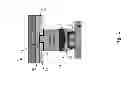
Referring now to FIG. 2, the metal bump 16 may be a vertical bump. As such, sidewalls 36 of the metal bump 16 may be vertical (as oriented in FIG. 2). In such an embodiment, a top width 40 of the metal bump 16 is the same as a bottom width 38. As shown in FIG. 2, in an embodiment a metal oxide 42 (e.g., cupric oxide, CuO, cuprous oxide, Cu2O, aluminum oxide, Al2O3, etc.) is formed on the sidewalls 36 of the metal bump 16.
As shown in FIG. 3, the metal bump 16 may also be a ladder bump. As such, the metal bump 16 has a sloped or tapering profile. Indeed, the metal bump 16 generally has the shape of a truncated cone. In an embodiment, the sidewalls 36 of the metal bump 16 are linear from a distal end (which is closest to the conglomeration 34) to a mounted end of the metal bump 16 along an entire height (i.e., or length) of the sidewalls 36. As shown in FIG. 3, in an embodiment the metal bump 16 also includes the metal oxide 42 on the sidewalls 36. The metal oxide 42 may provide better adhesion with molding or underfill material relative to uncoated sidewalls.
Still referring to FIG. 3, in an embodiment the bottom width 38 of the metal bump 16, which is closest to the integrated circuit 26 (FIG. 1), is larger than the top width 40 of the metal bump 16, which is furthest from the integrated circuit 26. In an embodiment, the top width 40 is between about 10 μm to about 80 μm. In an embodiment, the bottom width 38 is between about 20 μm to about 90 μm. In an embodiment, the ratio of the top width 40 to the bottom width 38 of the metal bump 16 in FIG. 3 is between about 0.5 and about 0.89.
One skilled in the art will recognize that the specific dimensions for the various widths and spacing discussed herein are matters of design choice and are dependent upon the particular technology node, and application employed.
In an embodiment, a photolithography process is used to shape the metal bump 16 as shown in FIG. 3. Indeed, in the photolithography process a photoresist may be shaped appropriately in order to produce the metal bump 16 in the form illustrated in FIG. 3. In an embodiment, the metal bump 16 may be formed using an electrolytic plating process.
Referring now to FIG. 4, a periphery of the metal bump 16 may take or resemble a variety of different shapes when viewed from above. In an embodiment, the metal bump 16 is in the form of a circle, a rectangle, an ellipse, an obround, a hexagon, an octagon, a trapezoid, a diamond, a capsule, and combinations thereof when viewed from the end mounted to the integrated circuit 26 in FIG. 1. In FIG. 4, the periphery of the metal bump 16 is shown relative to the underlying metal substrate trace 18 of FIG. 1.
Referring now to FIG. 5, an embodiment method 50 of forming the BOT structure 10 of FIG. 1 is provided. In block 52, the contact element 12 is formed over the integrated circuit 26. In block 54, the UBM feature 14 is electrically coupled to the contact element 12. In block 56, the metal bump 16 is mounted on the UBM feature 14. In block 58, the substrate trace 18 is mounted on the substrate 20. In block 60, the substrate trace 18 is mounted to the metal bump 16 using the solder joint 22 and the intermetallic compounds 24 such that the ratio of a cross sectional area of the intermetallic compounds 24 to a cross sectional area of the solder joint 22 is greater than forty percent.
From the foregoing it should be recognized that embodiment BOT structure 10 provides advantageous features. For example, the BOT assembly 10 permits fine pitch configurations while still providing an increased electromigration resistance due to the conglomeration 34 of the solder joint 22 and the IMCs 24, which has lower diffusivity compared to only solder. Therefore, the time to electromigration failure is slower.
The following references are related to subject matter of the present application. Each of these references is incorporated herein by reference in its entirety:
-
- U.S. Publication No. 2011/0285023 of Shen, et al. filed on Nov. 24, 2011, entitled “Substrate Interconnections Having Different Sizes.”
An embodiment bump on trace (BOT) structure includes a contact element supported by an integrated circuit, an under bump metallurgy (UBM) feature electrically coupled to the contact element, a metal bump on the under bump metallurgy feature, and a substrate trace on a substrate, the substrate trace coupled to the metal bump through a solder joint and intermetallic compounds, a ratio of a first cross sectional area of the intermetallic compounds to a second cross sectional area of the solder joint greater than forty percent.
An embodiment bump on trace (BOT) structure including a contact element supported by an integrated circuit, an under bump metallurgy (UBM) feature electrically coupled to the contact element, a metal bump on the under bump metallurgy feature, a substrate trace on a substrate, intermetallic compounds on the metal bump and on the substrate trace, and a solder joint formed between the intermetallic compounds disposed on the metal bump and on the substrate trace, a ratio of a first cross sectional area of the intermetallic compounds to a second cross sectional area of the solder joint greater than forty percent.
An embodiment method of forming a bump on trace (BOT) structure includes forming a contact element over an integrated circuit, electrically coupling an under bump metallurgy (UBM) feature to the contact element, forming a metal bump on the under bump metallurgy feature, forming a substrate trace on a substrate, and coupling the substrate trace to the metal bump using a solder joint, wherein intermetallic compounds are formed between the substrate trace and the metal bump, a ratio of a first cross sectional area of the intermetallic compounds to a second cross sectional area of the solder joint greater than forty percent.
While this invention has been described with reference to illustrative embodiments, this description is not intended to be construed in a limiting sense. Various modifications and combinations of the illustrative embodiments, as well as other embodiments of the invention, will be apparent to persons skilled in the art upon reference to the description. It is therefore intended that the appended claims encompass any such modifications or embodiments.
Claims
What is claimed is:1. A bump on trace (BOT) structure, comprising:
a contact element supported by an integrated circuit;
an under bump metallurgy (UBM) feature electrically coupled to the contact element;
a metal bump on the under bump metallurgy feature; and
a substrate trace on a substrate, the substrate trace coupled to the metal bump through a solder joint and intermetallic compounds, a ratio of a first cross sectional area of the intermetallic compounds to a second cross sectional area of the solder joint greater than forty percent.
2. The structure of claim 1, wherein the metal bump has a non-tapering profile.
3. The structure of claim 1, wherein a bottom width of the metal bump is equal to a top width of the metal bump.
4. The structure of claim 1, wherein the metal bump has a tapering profile.
5. The structure of claim 1, wherein a bottom width of the metal bump is greater than a top width of the metal bump.
6. The structure of claim 1, wherein a ratio of a top width of the metal bump to a bottom width of the metal bump is between about 0.5 to about 0.89.
7. The structure of claim 1, wherein the first tapering profile of the metal bump is linear.
8. The structure of claim 1, wherein sidewalls of the metal bump are coated with a metal oxide.
9. The structure of claim 1, wherein a periphery of the metal bump resembles one of a circle, a rectangle, an ellipse, an obround, a hexagon, an octagon, a trapezoid, a diamond, a capsule, and combinations thereof when viewed from a mounted end.
10. The structure of claim 1, wherein the substrate trace is provided with a surface treatment.
11. The structure of claim 1, wherein the substrate trace is coupled to the metal bump through the solder joint, intermetallic compounds, and an additional metal, the additional metal interposed between the metal bump and the solder joint.
12. A bump on trace (BOT) structure, comprising:
a contact element supported by an integrated circuit;
an under bump metallurgy (UBM) feature electrically coupled to the contact element;
a metal bump on the under bump metallurgy feature;
a substrate trace on a substrate;
intermetallic compounds disposed on the metal bump and on the substrate trace; and
a solder joint formed between the intermetallic compounds on the metal bump and on the substrate trace, a ratio of a first cross sectional area of the intermetallic compounds to a second cross sectional area of the solder joint greater than forty percent.
13. The structure of claim 12, wherein the metal bump has a tapering profile.
14. The structure of claim 12, wherein a ratio of a top width of the metal bump to a bottom width of the metal bump is between about 0.5 to about 0.89.
15. The structure of claim 12, wherein sidewalls of the metal bump are coated with a metal oxide.
16. The structure of claim 12, wherein the substrate trace is provided with a surface treatment, the surface treatment one of an organic solderability preservative (OSP) and an immersion tin (IT).
17. A method of forming a bump on trace (BOT) structure, comprising:
forming a contact element over an integrated circuit;
electrically coupling an under bump metallurgy (UBM) feature to the contact element;
forming a metal bump on the under bump metallurgy feature;
forming a substrate trace on a substrate; and
coupling the substrate trace to the metal bump using a solder joint, wherein intermetallic compounds are formed between the substrate trace and the metal bump, a ratio of a first cross sectional area of the intermetallic compounds to a second cross sectional area of the solder joint greater than forty percent.
18. The method of claim 17, further comprising inserting an additional metal between the metal bump and the solder joint.
19. The method of claim 18, wherein the additional metal is nickel.
20. The method of claim 17, wherein the metal bump has a tapering profile and metal oxide on sidewalls.
Images & Drawings included:


Sources:
- United States Patent and Trademark Office - verify current appl. status at the USPTO↗
Similar patent applications:
- » 20070252272
Bump structure, method of forming bump structure, and semiconductor apparatus using the same - » 20130292822
Bump structure, having concave lateral sides, semiconductor package having the bump structure, and method of forming the bump structure - » 20190096836
BUMP STRUCTURE, SEMICONDUCTOR PACKAGE INCLUDING THE BUMP STRUCTURE, AND METHOD OF FORMING THE BUMP STRUCTURE - » 20110006416
Structure and method for forming pillar bump structure having sidewall protection - » 20050208751
Solder bump structure and method for forming a solder bump - » 10339456
Solder bump structure and method for forming a solder bump - » 20070228559
Connecting structure, method for forming bump, and method for producing device-mounting substrate - » 10825199
Reinforced solder bump structure and method for forming a reinforced solder bump - » 20110127668
Semiconductor Device and Method of Forming Bump Structure with Multi-Layer UBM Around Bump Formation Area - » 20060113681
Reinforced solder bump structure and method for forming a reinforced solder bump
Recent applications in this class:
- » 20250273612 2025-08-28
PACKAGE COMPRISING A SUBSTRATE INCLUDING AN INTER SUBSTRATE INTERCONNECT STRUCTURE COMPRISING AN INNER INTERCONNECT - » 20250266383 2025-08-21
CONDUCTIVE BUMP STRUCTURE AND MANUFACTURING METHOD THEREOF - » 20250259954 2025-08-14
SOLDER BALL, SEMICONDUCTOR PACKAGE INCLUDING THE SAME, AND METHOD OF MANUFACTURING THE SAME - » 20250259953 2025-08-14
SEMICONDUCTOR PACKAGE - » 20250226344 2025-07-10
CORE BALL AND SEMICONDUCTOR PACKAGE INCLUDING THE SAME - » 20250226343 2025-07-10
ELECTRONIC DEVICE - » 20250218997 2025-07-03
COPPER PILLAR BUMP STRUCTURE AND METHOD OF MANUFACTURING THE SAME - » 20250218996 2025-07-03
COPPER PILLAR BUMP STRUCTURE AND METHOD OF MANUFACTURING THE SAME - » 20250218995 2025-07-03
COPPER PILLAR BUMP STRUCTURE AND METHOD OF MANUFACTURING THE SAME - » 20250218994 2025-07-03
COPPER PILLAR BUMP STRUCTURE AND METHOD OF MANUFACTURING THE SAME
Recent applications for this Assignee:
- » 20240266341 2024-08-08
HYBRID BONDING WITH UNIFORM PATTERN DENSITY - » 20240224489 2024-07-04
SEMICONDUCTOR DEVICE - » 20240170063 2024-05-23
CONTENT ADDRESSABLE MEMORY ARRAY DEVICE STRUCTURE - » 20240161819 2024-05-16
MEMORY DEVICE AND MANUFACTURING THEREOF - » 20240153896 2024-05-09
SEMICONDUCTOR PACKAGE SYSTEM AND METHOD - » 20240120409 2024-04-11
Method for non-resist nanolithography - » 20240113080 2024-04-04
Semiconductor Device with Discrete Blocks - » 20240105632 2024-03-28
Method for forming a semiconductor device including forming a first interconnect structure on one side of a substrate having first metal feature closer the substrate than second metal feature and forming first and second tsv on other side of substrate connecting to the metal features - » 20240096816 2024-03-21
Method of manufacture overlay mark using laser marking process for semiconductor device - » 20240096383 2024-03-21
MEMORY DEVICE