Package structure and method for manufacturing package structure
US20140097545A1
2014-04-10
14/044,819
2013-10-02
✅ Patent granted
US 9,466,553 B2
2016-10-11
-
-
Nicholas Tobergte
NSIP Law
2033-10-02
Abstract:
Disclosed herein is a method for manufacturing a package structure. According to an exemplary embodiment of the present invention, the method for manufacturing a package structure includes: preparing a die having a metal pillar disposed on one surface thereof; bonding the die on the metal plate to allow the metal pillar to face the outside; forming an insulating film covering the metal plate and the die; buffing the insulating film so as to expose the metal pillar; and manufacturing a first package structure by forming a circuit structure electrically connected to the metal pillar on the insulating film.
Inventors:
- Heung Ku Kim 1 🇰🇷 Chungcheongnam-do, South Korea
- Heung Ku Kim 1 🇰🇷 Yeongi-gun, South Korea
Assignee:
- SAMSUNG ELECTRO-MECHANICS CO., LTD. 5,757 🇰🇷 Suwon-si, South Korea
- SAMSUNG ELECTRO-MECHANICS CO., LTD. 293 🇰🇷 Gyeonggi-do, South Korea
Applicant:
Interested in similar patents?
Get notified when new applications in this technology area are published.
Classification:
H01L21/50 » CPC further
Processes or apparatus adapted for the manufacture or treatment of semiconductor or solid state devices or of parts thereof; Manufacture or treatment of semiconductor devices or of parts thereof the devices having at least one potential-jump barrier or surface barrier, e.g. PN junction, depletion layer or carrier concentration layer Assembly of semiconductor devices using processes or apparatus not provided for in a single one of the subgroups - , e.g. sealing of a cap to a base of a container
H01L23/481 » CPC main
Details of semiconductor or other solid state devices; Arrangements for conducting electric current to or from the solid state body in operation, e.g. leads, terminal arrangements ; Selection of materials therefor Internal lead connections, e.g. via connections, feedthrough structures
H01L23/48 IPC
Details of semiconductor or other solid state devices Arrangements for conducting electric current to or from the solid state body in operation, e.g. leads, terminal arrangements ; Selection of materials therefor
H01L25/50 » CPC further
Assemblies consisting of a plurality of individual semiconductor or other solid state devices ; Multistep manufacturing processes thereof Multistep manufacturing processes of assemblies consisting of devices, each device being of a type provided for in group or
H01L23/49822 » CPC further
Details of semiconductor or other solid state devices; Arrangements for conducting electric current to or from the solid state body in operation, e.g. leads, terminal arrangements ; Selection of materials therefor consisting of soldered constructions; Leads, on insulating substrates, Multilayer substrates
H01L23/5389 » CPC further
Details of semiconductor or other solid state devices; Arrangements for conducting electric current within the device in operation from one component to another, i.e. interconnections, e.g. wires, lead frames the interconnection structure between a plurality of semiconductor chips being formed on, or in, insulating substrates the chips being integrally enclosed by the interconnect and support structures
H01L24/19 » CPC further
Arrangements for connecting or disconnecting semiconductor or solid-state bodies; Methods or apparatus related thereto; Means for bonding being attached to, or being formed on, the surface to be connected, e.g. chip-to-package, die-attach, "first-level" interconnects; Manufacturing methods related thereto; High density interconnect [HDI] connectors; Manufacturing methods related thereto Manufacturing methods of high density interconnect preforms
H01L24/20 » CPC further
Arrangements for connecting or disconnecting semiconductor or solid-state bodies; Methods or apparatus related thereto; Means for bonding being attached to, or being formed on, the surface to be connected, e.g. chip-to-package, die-attach, "first-level" interconnects; Manufacturing methods related thereto; High density interconnect [HDI] connectors; Manufacturing methods related thereto Structure, shape, material or disposition of high density interconnect preforms
H01L25/00 IPC
Assemblies consisting of a plurality of individual semiconductor or other solid state devices ; Multistep manufacturing processes thereof
H01L23/3114 » CPC further
Details of semiconductor or other solid state devices; Encapsulations, e.g. encapsulating layers, coatings, e.g. for protection characterised by the arrangement or shape the device being completely enclosed the device being a chip scale package, e.g. CSP
H01L24/13 » CPC further
Arrangements for connecting or disconnecting semiconductor or solid-state bodies; Methods or apparatus related thereto; Means for bonding being attached to, or being formed on, the surface to be connected, e.g. chip-to-package, die-attach, "first-level" interconnects; Manufacturing methods related thereto; Bump connectors ; Manufacturing methods related thereto; Structure, shape, material or disposition of the bump connectors prior to the connecting process of an individual bump connector
H01L24/16 » CPC further
Arrangements for connecting or disconnecting semiconductor or solid-state bodies; Methods or apparatus related thereto; Means for bonding being attached to, or being formed on, the surface to be connected, e.g. chip-to-package, die-attach, "first-level" interconnects; Manufacturing methods related thereto; Bump connectors ; Manufacturing methods related thereto; Structure, shape, material or disposition of the bump connectors after the connecting process of an individual bump connector
H01L25/105 » CPC further
Assemblies consisting of a plurality of individual semiconductor or other solid state devices ; Multistep manufacturing processes thereof all the devices being of a type provided for in the same subgroup of groups - , e.g. assemblies of rectifier diodes the devices having separate containers the devices being of a type provided for in group
H01L2224/0401 » CPC further
Indexing scheme for arrangements for connecting or disconnecting semiconductor or solid-state bodies and methods related thereto as covered by; Means for bonding being attached to, or being formed on, the surface to be connected, e.g. chip-to-package, die-attach, "first-level" interconnects; Manufacturing methods related thereto; Bonding areas; Manufacturing methods related thereto; Structure, shape, material or disposition of the bonding areas prior to the connecting process Bonding areas specifically adapted for bump connectors, e.g. under bump metallisation [UBM]
H01L2224/04105 » CPC further
Indexing scheme for arrangements for connecting or disconnecting semiconductor or solid-state bodies and methods related thereto as covered by; Means for bonding being attached to, or being formed on, the surface to be connected, e.g. chip-to-package, die-attach, "first-level" interconnects; Manufacturing methods related thereto; Bonding areas; Manufacturing methods related thereto; Structure, shape, material or disposition of the bonding areas prior to the connecting process Bonding areas formed on an encapsulation of the semiconductor or solid-state body, e.g. bonding areas on chip-scale packages
H01L2224/12105 » CPC further
Indexing scheme for arrangements for connecting or disconnecting semiconductor or solid-state bodies and methods related thereto as covered by; Means for bonding being attached to, or being formed on, the surface to be connected, e.g. chip-to-package, die-attach, "first-level" interconnects; Manufacturing methods related thereto; Bump connectors; Manufacturing methods related thereto; Structure, shape, material or disposition of the bump connectors prior to the connecting process Bump connectors formed on an encapsulation of the semiconductor or solid-state body, e.g. bumps on chip-scale packages
H01L2224/73259 » CPC further
Indexing scheme for arrangements for connecting or disconnecting semiconductor or solid-state bodies and methods related thereto as covered by; Means for bonding being of different types provided for in two or more of groups; Location after the connecting process on different surfaces Bump and HDI connectors
H01L2225/1035 » CPC further
Details relating to assemblies covered by the group but not provided for in its subgroups; All the devices being of a type provided for in the same subgroup of groups - the devices having separate containers the devices being of a type provided for in group the containers being in a stacked arrangement the lowermost container comprising a device support the device being entirely enclosed by the support, e.g. high-density interconnect [HDI]
H01L2225/1058 » CPC further
Details relating to assemblies covered by the group but not provided for in its subgroups; All the devices being of a type provided for in the same subgroup of groups - the devices having separate containers the devices being of a type provided for in group the containers being in a stacked arrangement; Details of electrical connections between containers Bump or bump-like electrical connections, e.g. balls, pillars, posts
H01L2924/00014 » CPC further
Indexing scheme for arrangements or methods for connecting or disconnecting semiconductor or solid-state bodies as covered by; Technical content checked by a classifier the subject-matter covered by the group, the symbol of which is combined with the symbol of this group, being disclosed without further technical details
H01L2924/15331 » CPC further
Indexing scheme for arrangements or methods for connecting or disconnecting semiconductor or solid-state bodies as covered by; Details of package parts other than the semiconductor or other solid state devices to be connected; Die mounting substrate; Connection portion the connection portion being formed on the die mounting surface of the substrate the connection portion being formed both on the die mounting surface of the substrate and outside the die mounting surface of the substrate being a ball array, e.g. BGA
H01L2924/181 » CPC further
Indexing scheme for arrangements or methods for connecting or disconnecting semiconductor or solid-state bodies as covered by; Details of package parts other than the semiconductor or other solid state devices to be connected Encapsulation
H01L2924/18162 » CPC further
Indexing scheme for arrangements or methods for connecting or disconnecting semiconductor or solid-state bodies as covered by; Details of package parts other than the semiconductor or other solid state devices to be connected; Encapsulation; Shape; Exposing the passive side of the semiconductor or solid-state body of a chip with build-up interconnect
H01L23/00 IPC
Details of semiconductor or other solid state devices
H01L25/03 » CPC further
Assemblies consisting of a plurality of individual semiconductor or other solid state devices ; Multistep manufacturing processes thereof all the devices being of a type provided for in the same subgroup of groups - , e.g. assemblies of rectifier diodes
H01L23/498 IPC
Details of semiconductor or other solid state devices; Arrangements for conducting electric current to or from the solid state body in operation, e.g. leads, terminal arrangements ; Selection of materials therefor consisting of soldered constructions Leads, on insulating substrates,
H01L23/538 IPC
Details of semiconductor or other solid state devices; Arrangements for conducting electric current within the device in operation from one component to another, i.e. interconnections, e.g. wires, lead frames the interconnection structure between a plurality of semiconductor chips being formed on, or in, insulating substrates
H01L23/31 IPC
Details of semiconductor or other solid state devices; Encapsulations, e.g. encapsulating layers, coatings, e.g. for protection characterised by the arrangement or shape
H01L25/10 IPC
Assemblies consisting of a plurality of individual semiconductor or other solid state devices ; Multistep manufacturing processes thereof all the devices being of a type provided for in the same subgroup of groups - , e.g. assemblies of rectifier diodes the devices having separate containers
H01L24/81 » CPC further
Arrangements for connecting or disconnecting semiconductor or solid-state bodies; Methods or apparatus related thereto; Methods for connecting semiconductor or other solid state bodies using means for bonding being attached to, or being formed on, the surface to be connected using a bump connector
H01L23/49816 » CPC further
Details of semiconductor or other solid state devices; Arrangements for conducting electric current to or from the solid state body in operation, e.g. leads, terminal arrangements ; Selection of materials therefor consisting of soldered constructions; Leads, on insulating substrates,; Additional leads joined to the metallisation on the insulating substrate, e.g. pins, bumps, wires, flat leads Spherical bumps on the substrate for external connection, e.g. ball grid arrays [BGA]
H01L2924/15311 » CPC further
Indexing scheme for arrangements or methods for connecting or disconnecting semiconductor or solid-state bodies as covered by; Details of package parts other than the semiconductor or other solid state devices to be connected; Die mounting substrate; Connection portion the connection portion being formed only on the surface of the substrate opposite to the die mounting surface being a ball array, e.g. BGA
Description
This application claims the benefit under 35 U.S.C. Section 119 of Korean Patent Application Serial No. 10-2012-0111198 entitled “Package Structure And Method For Manufacturing Package Structure” filed on Oct. 8, 2012, which is hereby incorporated by reference in its entirety into this application.
BACKGROUND OF THE INVENTION
1. Technical Field
The present invention relates to a package structure and a method for manufacturing the same, and more particularly, to a package structure with improved manufacturing efficiency and a method for manufacturing the same.
2. Description of the Related Art
With the development of a high-density and high-performance semiconductor package, various package technologies have been developed. As the semiconductor package technologies, there is a package technology which bonds a die to a circuit board using a non-conductive paste (NCP). In more detail, the semiconductor package is manufactured by bonding a die to a circuit board while connecting a copper pillar and a metal bump to be aligned with each other, after the die having a copper (Cu) pillar disposed on one surface thereof and the circuit board having a metal bump disposed on one surface thereof are prepared and a non-conductive paste is interposed between the die and the circuit board.
However, in the case of the package technology using the non-conductive paste, a phenomenon that the non-conductive paste is not completely filled between the circuit board and the bump at the time of the packaging occurs. In this case, voids occur within the non-conductive paste, which is a cause of the occurrence of short between circuit patterns of the semiconductor package. Further, when a pitch between the metal pillars of the die is fine, it is difficult to match the metal pillars with the metal bumps, which causes the packaging defect.
RELATED ART DOCUMENT
Patent Document
- (Patent Document 1) Korean Patent Laid-Open Publication No. 10-2011-0070924
SUMMARY OF THE INVENTION
An object of the present invention is to provide a package structure with improved manufacturing efficiency and a method for manufacturing the same.
Another object of the present invention is to provide a package structure capable of solving problems occurring at the time of using a non-conductive paste and a method for manufacturing the same.
According to an exemplary embodiment of the present invention, there is provided a package structure, including: a metal plate; a die bonded to the metal plate to allow a metal pillar so as to face the outside; an insulating film covering the metal plate and the die so as to expose the metal pillar; and a metal pattern electrically connected to the metal pillar on the insulating film.
The circuit structure may be formed by performing a plating process on the insulating film.
The insulating film may be formed by directly laminating the insulating film on the metal plate and the die.
According to another exemplary embodiment of the present invention, there is provided a method for manufacturing a package structure, including: preparing a die having a metal pillar disposed on one surface thereof; bonding the die on the metal plate to allow the metal pillar to face the outside; forming an insulating film covering the metal plate and the die; buffing the insulating film so as to expose the metal pillar; and manufacturing a first package structure by forming a circuit structure electrically connected to the metal pillar on the insulating film.
The forming of the circuit structure includes: forming a metal seed layer covering the insulating film; forming an anti-plating pattern on the metal seed layer; forming a plating film on the metal seed layer by using the anti-plating pattern as an anti-plating film; and removing the anti-plating pattern.
The method for manufacturing a package structure may further include: forming a metal pattern by removing a part of the metal plate so as to expose the die; preparing a second package structure in which an external connection terminal is formed; and laminating the second package structure on the first package structure, while bonding the external connection terminal to the metal pattern.
The preparing of the die may include preparing a semiconductor integrated circuit chip having an inner via, and the method for manufacturing a package structure may further include: removing the metal plate so as to expose the die; and laminating an additional die on the exposed die.
The forming of the insulating film may include directly laminating the insulating film on the metal plate and the die.
BRIEF DESCRIPTION OF THE DRAWINGS
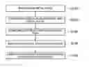
FIG. 1 is a flow chart showing a method for manufacturing a package structure according to an exemplary embodiment of the present invention.
FIGS. 2 to 5 are views describing a process of manufacturing a package structure according to the exemplary embodiment of the present invention.
FIG. 6 is a flow chart illustrating a package structure according to a modified example of the present invention.
FIGS. 7 and 8 are views describing a process of manufacturing a package structure according to a modified example of the present invention.
DESCRIPTION OF THE PREFERRED EMBODIMENTS
Various advantages and features of the present invention and methods accomplishing thereof will become apparent from the following description of embodiments with reference to the accompanying drawings. However, the present invention may be modified in many different forms and it should not be limited to exemplary embodiments set forth herein. Rather, these embodiments may be provided so that this disclosure will be thorough and complete, and will fully convey the scope of the invention to those skilled in the art. Like reference numerals throughout the specification denote like elements.
Terms used in the present specification are for explaining the embodiments rather than limiting the present invention. Unless explicitly described to the contrary, a singular form includes a plural form in the present specification. The word “comprise” and variations such as “comprises” or “comprising,” will be understood to imply the inclusion of stated constituents, steps, operations and/or elements but not the exclusion of any other constituents, steps, operations and/or elements.
Further, the exemplary embodiments described in the specification will be described with reference to cross-sectional views and/or plan views that are ideal exemplification figures. In drawings, the thickness of layers and regions is exaggerated for efficient description of technical contents. Therefore, exemplified forms may be changed by manufacturing technologies and/or tolerance. Therefore, the exemplary embodiments of the present invention are not limited to specific forms but may include the change in forms generated according to the manufacturing processes For example, an etching region vertically shown may be rounded or may have a predetermined curvature.
Hereinafter, a package structure and a method for manufacturing the same according to exemplary embodiments of the present invention will be described in detail with reference to the accompanying drawings.
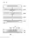
FIG. 1 is a flow chart showing a method for manufacturing a package structure according to an exemplary embodiment of the present invention and FIGS. 2 to 5 are views describing a process of manufacturing a package structure according to the exemplary embodiment of the present invention.
Referring to FIGS. 1 and 2, a die 110 may be bonded on a metal plate 120 (S110). In detail, the die 110 may be prepared. In the preparing of the die 110, a semiconductor integrated circuit chip 112 having one surface 112a on which a metal pillar 114 is formed and the other surface 112b which is an opposite surface to the one surface may be prepared. The metal pillar 114 may be made of a copper material. Meanwhile, the metal plate 120 may be prepared. As the metal plate 120, a thin plate made of the copper material having relatively high thermal conductivity may be used. Further, the other surface 112b of the die 110 may be bonded on the metal plate 120 to allow the metal pillar 114 to face the outside.
An insulating film 130 which covers the die 110 and the metal plate 120 may be formed (S120). The forming of the insulating film 130 may include laminating the insulating film covering the die 110 and the metal plate 120, along with the metal pillar 114 and polishing or buffing the insulating film 130 so as to expose the metal pillar 114 and a part of the metal plate 120. Herein, the directly laminating of the insulating film 130 may be defined as directly covering the insulating film 130 on the die 110 and the metal plate 120, without using intermediate materials, such as a non-conductive paste (NCP). Therefore, the die 110 and the metal plate 120 are covered on the metal plate 120, but the insulating film 130 having a via hole 132 through which the metal pillar 114 is exposed and at the same time, a part of the metal plate 120 is exposed may be formed.
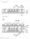
Referring to FIGS. 1 and 3, a circuit structure 140 may be formed on the insulating film 130 (S130). The forming of the circuit structure 140 may include forming a metal seed layer (not illustrated) on the insulating film 130, forming an anti-plating pattern (not illustrated) on the metal seed layer, forming a plating film by performing a plating process using the anti-plating pattern as an anti-plating film, and removing the anti-plating pattern. Therefore, a metal via 142 formed in the via hole 132 of the insulating film 130 may be formed on the insulating film 130 and a circuit pattern 144 electrically connected to the metal pillar 114 may be formed on the insulating film 130.
Referring to FIGS. 1 and 4, a first package structure 101 may be manufactured (S140). The manufacturing of the first package structure 101 may be performed by further forming a circuit substrate layer 150 on results previously illustrated in FIG. 3. The forming of the circuit substrate layer 150 may include forming an outside layer 152 made of an insulating material on the results described above with reference to FIG. 3, forming a wiring structure 154 configured of a conductive via, a circuit pattern, and the like, on the outside layer 152, forming a solder resist pattern 156 exposing the wiring structure 154 on the outside layer 152, and bonding an external connection terminal 158 to the wiring structure 154 exposed by the solder resist pattern 156. As the external connection terminal 158, a solder ball may be used. By the above described process, the first package structure 101 in which the die 110 having the metal pillar 114 is packaged may be manufactured, without using the non-conductive paste (NCP).
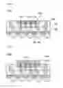
Referring to FIGS. 1 and 5, a second package structure 102 may be laminated on the first package structure 101 (S150). For example, the second package structure 102 may be prepared. The second package structure 102 may include a circuit board on which the connection terminal 102a is formed. A metal pattern 121 for electrical connection of the second package structure 102 may be formed by removing a part of the metal plate 120 of FIG. 4 so as to expose the other surface 112b of the die 110 of the first package structure 101. Further, the connection terminal 102a of the second package structure 102 may be bonded to the metal pattern 121 of the first package structure 101. Therefore, the package structure 100 in a package on package (POP) type may be manufactured.
As described above, a method for manufacturing a package structure according to the exemplary embodiment of the present invention may manufacture a package substrate by disposing the die 110 having the metal pillar 114 on the metal plate 120. In this case, compared to a technology of packaging the die having the metal pillar by using the non-conductive paste, the occurrence problem of voids occurring at the time of using the non-conductive paste may be solved and a heat radiating effect of the die 110 may be improved. Therefore, according to the package structure and the method for manufacturing the same according to the exemplary embodiments of the present invention, the packaging may be implemented by bonding the die having the metal pillar on the metal plate without using the non-conductive paste, thereby preventing the voids from occurring within the insulating film at the time of using the non-conductive paste and improving the heat radiating effect of the die.
The method for manufacturing a package structure according to the exemplary embodiment of the present invention may form the circuit structure 140 on the insulating layer 130 after the die 110 having the metal pillar 114 is disposed on the metal plate 120 and the insulating film 130 covering the metal pillar 114 and the die 110 is directly laminated. In this case, compared to the case of bonding the die to the substrate by interposing the non-conductive paste therebetween, the matching degree of the die 110 and the circuit structure 140 may increase, which may be very advantageous in the packaging of the die having the metal pillar of a pine pitch. Therefore, according to the package structure and the method for manufacturing the same according to the exemplary embodiments of the present invention, the matching degree of the metal pillar and the circuit structure may be improved by forming the circuit structure electrically connected to the metal pillar after directly laminating the insulating film on the die having the metal pillar without using the non-conductive paste.
According to the method for manufacturing a package structure according to the exemplary embodiment of the present invention, the second package structure 102 may be laminated on the first package structure 101 in the state in which the other surface of the die 110 is exposed to the outside, without using a separate protective film, such as an epoxy molding compound (EMC). In this case, the package structure 100 may be manufactured without using the separate protective film, in the state in which the die 110 disposed in the first package structure 101 is exposed to the outside. Further, according to the method for manufacturing a package structure according to the exemplary embodiments of the present invention, the package structure in the package on package (POP) type may be manufactured without covering the die with the separate protective film, such as the epoxy molding compound, thereby more reducing the overall thickness of the package structure and more improving the heat radiating effect of the die as compared with the case of using the protective film. Further, according to the package structure and the method for manufacturing a package structure according to the exemplary embodiments of the present invention, the metal pillar of the die may be partially etched, thereby implementing the thinner package on package.
Hereinafter, a method for manufacturing a package structure according to a modified example of the present invention will be described in detail. Herein, a description of overlapping portions with the method for manufacturing a package structure according to the exemplary embodiment of the present invention described above will be omitted or simplified.
FIG. 6 is a flow chart illustrating a package structure according to a modified example of the present invention and FIGS. 7 to 8 are views describing a process of manufacturing a package structure according to a modified example of the present invention.
Referring to FIGS. 6 and 7, a reserved package structure illustrated in FIG. 3 may be prepared (S210). The preparing of the reserved package structure may be similar to one described above with reference to FIGS. 2 and 3. However, the die 110a to be packaged may have an inner via 116 electrically connected to the metal pillar 114 on the one surface 112a thereof, while penetrating through the one surface 112a and the other surface 112b of the die 110a. The die 110a having the above-mentioned structure may be the semiconductor integrated circuit chip having a through silicon via (TSA) structure. The inner via 116 may be manufactured during the process of manufacturing the die 110a. As another example, the inner via 116 may be directly formed on the die 110a after the metal plate 120 is removed as described above.
Further, the package structure 101a may be manufactured by removing the metal plate of the reserved package structure (S220). The removing of the metal plate may be performed by performing a predetermined etching process on the metal plate 120 so as to expose the other surface 112b of the die 110a and the metal via 144 of the circuit structure 140. Therefore, the package structure 101a in which the inner via 116 of the die 110a is exposed to the outside may be manufactured.
Referring to FIGS. 6 and 8, the additional die 110b may be bonded to the package structure 101a (S230). The bonding of the additional die 110b may include performing an electrical inspection on the die 110a, preparing a semiconductor integrated circuit chip having a connection terminal 110b′ disposed on one surface thereof, and bonding the additional die 110b to the die 110a so that the connection terminal 110b′ is electrically connected to the inner via 116 of the die 110a. When the defect of the die 110a occurs during the performing of the electrical inspection on the die 110a, a new die may be replaced or a performance of a subsequent process may be retained. Therefore, the package structure 101a having a structure in which the two dies 110a and 110b are laminated may be manufactured.
By the above-mentioned process, the package structure 100a having a structure in which the plurality of dies 110a and 110b are laminated may be manufactured. The package structure 100a may solve a part of the known good die (KGD) which is a disadvantage of the through silicon via, by mounting the additional die after manufacturing the package using the through silicon via (STA) die and completing the electrical inspection thereon. Further, according to the method for manufacturing a package structure according to the exemplary embodiments of the present invention, the semiconductor package using the die having the through silicon via (TSV) structure can be implemented without using the non-conductive paste to solve the problem of the known good die (KGD) which is a disadvantage of the through silicon via package, thereby improving the manufacturing yield and the reducing the manufacturing costs.
According to the package structure and the method for manufacturing the same according to the exemplary embodiments of the present invention, the packaging can be implemented by bonding the die having the metal pillar on the metal plate without using the non-conductive paste, thereby preventing the voids from occurring within the insulating film at the time of using the non-conductive paste and improving the heat radiating effect of the die.
Further, according to the package structure and the method for manufacturing the same according to the exemplary embodiments of the present invention, the matching degree of the metal pillar and the circuit structure can be improved by forming the circuit structure electrically connected to the metal pillar after directly laminating the insulating film on the die having the metal pillar without using the non-conductive paste.
Further, according to the package structure and the method for manufacturing the same according to the exemplary embodiments of the present invention, the package structure in the package on package (POP) type can be manufactured without covering the die with the separate protective film, such as the epoxy molding compound, thereby more reducing the overall thickness of the package structure and more improving the heat radiating effect of the die as compared to the case of using the protective film. Further, according to the method for manufacturing a package structure according to the exemplary embodiments of the present invention, the metal pillar of the die can be partially etched, thereby implementing the thinner package on package.
Further, according to the package structure and the method for manufacturing the same according to the exemplary embodiments of the present invention, the semiconductor package using the die having the through silicon via (TSV) structure can be implemented without using the non-conductive paste to solve the problem of the known good die (KGD) which is a disadvantage of the through silicon via package, thereby improving the manufacturing yield and the reducing the manufacturing costs.
The present invention has been described in connection with what is presently considered to be practical exemplary embodiments. In addition, the above-mentioned description discloses only the exemplary embodiments of the present invention. Therefore, it is to be appreciated that modifications and alterations may be made by those skilled in the art without departing from the scope of the present invention disclosed in the present specification and an equivalent thereof. The exemplary embodiments described above have been provided to explain the best state in carrying out the present invention. Therefore, they may be carried out in other states known to the field to which the present invention pertains in using other inventions such as the present invention and also be modified in various forms required in specific application fields and usages of the invention. Therefore, it is to be understood that the invention is not limited to the disclosed embodiments. It is to be understood that other embodiments are also included within the spirit and scope of the appended claims.
Claims
What is claimed is:1. A package structure, comprising:
a metal plate;
a die bonded on the metal plate to allow a metal pillar so as to face the outside;
an insulating film covering the metal plate and the die so as to expose the metal pillar; and
a metal pattern electrically connected to the metal pillar on the insulating film.
2. The package structure according to claim 1, wherein the circuit structure is formed by performing a plating process on the insulating film.
3. The package structure according to claim 1, wherein the insulating film is formed by directly laminating the insulating film on the metal plate and the die.
4. A method for manufacturing a package structure, comprising:
preparing a die having a metal pillar disposed on one surface thereof;
bonding the die on the metal plate to allow the metal pillar to face the outside;
forming an insulating film covering the metal plate and the die;
buffing the insulating film so as to expose the metal pillar; and
manufacturing a first package structure by forming a circuit structure electrically connected to the metal pillar on the insulating film.
5. The method according to claim 4, wherein the forming of the circuit structure includes:
forming a metal seed layer covering the insulating film;
forming an anti-plating pattern on the metal seed layer;
forming a plating film on the metal seed layer by using the anti-plating pattern as an anti-plating film; and
removing the anti-plating pattern.
6. The method according to claim 4, further comprising:
forming a metal pattern by removing a part of the metal plate so as to expose the die;
preparing a second package structure in which an external connection terminal is formed; and
laminating the second package structure on the first package structure, while bonding the external connection terminal to the metal pattern.
7. The method according to claim 4, wherein the preparing of the die includes;
preparing a semiconductor integrated circuit chip having an inner via.
8. The method according to claim 4, wherein the method for manufacturing a package structure further includes:
removing the metal plate so as to expose the die; and
laminating an additional die on the exposed die.
9. The method according to any one of claims 4, wherein the forming of the insulating film includes directly laminating the insulating film on the metal plate and the die.
Images & Drawings included:

Sources:
- United States Patent and Trademark Office - verify current appl. status at the USPTO↗
Similar patent applications:
- » 20230064560
LIGHT EMITTING DIODE PACKAGE STRUCTURE, MANUFACTURING METHOD OF LIGHT EMITTING DIODE PACKAGE STRUCTURE AND LIGHT EMITTING PANEL - » 20130113099
Package carrier, package carrier manufacturing method, package structure for semiconductor device and manufacturing method thereof - » 20230048907
Integrated circuit, package structure, and manufacturing method of package structure - » 20220262758
Package structure and manufacturing method of package structure thereof - » 20210242159
Package structure and manufacturing method of package structure thereof - » 20170194241
Package structure and manufacturing method of package structure - » 20240071936
INTERPOSER SUBSTRATE, PACKAGE STRUCTURE AND MANUFACTURING METHOD OF PACKAGE STRUCTURE - » 20220068864
Integrated circuit, package structure, and manufacturing method of package structure - » 20200152847
LED package structure, heat-dissipating substrate, method for manufacturing LED package structure, and method for manufacturing heat-dissipating substrate - » 20090206472
COF packaging structure, method of manufacturing the COF packaging structure, and method for assembling a driver IC and the COF packaging structure thereof
Recent applications in this class:
- » 20250293121 2025-09-18
LOW COST EMBEDDED INTEGRATED CIRCUIT DIES - » 20250285942 2025-09-11
THROUGH SUBSTRATE VIA (TSV) VALIDATION STRUCTURE FOR AN INTEGRATED CIRCUIT AND METHOD TO FORM THE TSV VALIDATION STRUCTURE - » 20250285941 2025-09-11
LAYOUT METHOD AND MEMORY MACRO INCLUDING THROUGH-SILICON VIA - » 20250285940 2025-09-11
PRINTED CIRCUIT BOARD - » 20250266325 2025-08-21
Semiconductor Device Having Backside Interconnect Structure on Through Substrate Via - » 20250266324 2025-08-21
MANUFACTURING METHOD OF SEMICONDUCTOR PACKAGE - » 20250266323 2025-08-21
SEMICONDUCTOR DEVICE AND METHOD - » 20250266322 2025-08-21
SUBSTRATE COMPRISING VIAS AND ASSOCIATED MANUFACTURING METHODS - » 20250266321 2025-08-21
SEMICONDUCTOR DEVICE AND METHOD FOR MANUFACTURING THE SAME - » 20250259914 2025-08-14
SEMICONDUCTOR PACKAGE AND METHOD OF MANUFACTURING THE SAME
Recent applications for this Assignee:
- » 20250291200 2025-09-18
CAMERA MODULE - » 20250291156 2025-09-18
OPTICAL IMAGING SYSTEM - » 20250291155 2025-09-18
OPTICAL IMAGING SYSTEM - » 20250287502 2025-09-11
CIRCUIT BOARD AND MANUFACTURING METHOD THEREOF - » 20250287498 2025-09-11
PRINTED CIRCUIT BOARD - » 20250285957 2025-09-11
INTERPOSER SUBSTRATE AND SEMICONDUCTOR PACKAGE INCLUDING THE SAME - » 20250285940 2025-09-11
PRINTED CIRCUIT BOARD - » 20250284099 2025-09-11
OPTICAL IMAGING SYSTEM - » 20250284098 2025-09-11
LENS MODULE - » 20250284094 2025-09-11
OPTICAL IMAGING SYSTEM