Low profile electrical connector
US20150037985A1
2015-02-05
14/446,348
2014-07-30
✅ Patent granted
US 9,356,368 B2
2016-05-31
-
-
Abdullah Riyami | Vladimir Imas
Wei Te Chung | Ming Chieh Chang
2034-07-30
Abstract:
An electrical connector for electrically connecting a package with a printed circuit board (PCB) with a plurality of pads and an alignment feature includes an insulating housing, a plurality of contacts received in the insulating housing and a stiffener insert molding with the insulating housing. When the stiffener is assembled upon the alignment feature correspondingly, the contacts align with the pads of the PCB correspondingly.
Assignee:
- HON HAI PRECISION INDUSTRY CO., LTD. 10,014 🇹🇼 New Taipei, Taiwan
Applicant:
Interested in similar patents?
Get notified when new applications in this technology area are published.
Classification:
H01R12/7005 » CPC main
Structural associations of a plurality of mutually-insulated electrical connecting elements, specially adapted for printed circuits, e.g. printed circuit boards [PCBs], flat or ribbon cables, or like generally planar structures, e.g. terminal strips, terminal blocks; Coupling devices specially adapted for printed circuits, flat or ribbon cables, or like generally planar structures; Terminals specially adapted for contact with, or insertion into, printed circuits, flat or ribbon cables, or like generally planar structures; Coupling devices Guiding, mounting, polarizing or locking means; Extractors
H01R13/629 » CPC further
Details of coupling devices of the kinds covered by groups or -; Means for facilitating engagement or disengagement of coupling parts or for holding them in engagement Additional means for facilitating engagement or disengagement of coupling parts, e.g. aligning or guiding means, levers, gas pressure electrical locking indicators, manufacturing tolerances
H01R12/70 IPC
Structural associations of a plurality of mutually-insulated electrical connecting elements, specially adapted for printed circuits, e.g. printed circuit boards [PCBs], flat or ribbon cables, or like generally planar structures, e.g. terminal strips, terminal blocks; Coupling devices specially adapted for printed circuits, flat or ribbon cables, or like generally planar structures; Terminals specially adapted for contact with, or insertion into, printed circuits, flat or ribbon cables, or like generally planar structures Coupling devices
H01R12/707 » CPC main
Structural associations of a plurality of mutually-insulated electrical connecting elements, specially adapted for printed circuits, e.g. printed circuit boards [PCBs], flat or ribbon cables, or like generally planar structures, e.g. terminal strips, terminal blocks; Coupling devices specially adapted for printed circuits, flat or ribbon cables, or like generally planar structures; Terminals specially adapted for contact with, or insertion into, printed circuits, flat or ribbon cables, or like generally planar structures; Coupling devices; Guiding, mounting, polarizing or locking means; Extractors; Locking or fixing a connector to a PCB Soldering or welding
H01R12/7052 » CPC further
Structural associations of a plurality of mutually-insulated electrical connecting elements, specially adapted for printed circuits, e.g. printed circuit boards [PCBs], flat or ribbon cables, or like generally planar structures, e.g. terminal strips, terminal blocks; Coupling devices specially adapted for printed circuits, flat or ribbon cables, or like generally planar structures; Terminals specially adapted for contact with, or insertion into, printed circuits, flat or ribbon cables, or like generally planar structures; Coupling devices; Guiding, mounting, polarizing or locking means; Extractors; Locking or fixing a connector to a PCB characterised by the locating members
H01R4/04 » CPC further
Electrically-conductive connections between two or more conductive members in direct contact, i.e. touching one another; Means for effecting or maintaining such contact; Electrically-conductive connections having two or more spaced connecting locations for conductors and using contact members penetrating insulation using electrically conductive adhesives
H01R13/035 » CPC further
Details of coupling devices of the kinds covered by groups or -; Contact members characterised by the material, e.g. plating, or coating materials Plated dielectric material
H01R12/00 IPC
Structural associations of a plurality of mutually-insulated electrical connecting elements, specially adapted for printed circuits, e.g. printed circuit boards [PCBs], flat or ribbon cables, or like generally planar structures, e.g. terminal strips, terminal blocks; Coupling devices specially adapted for printed circuits, flat or ribbon cables, or like generally planar structures; Terminals specially adapted for contact with, or insertion into, printed circuits, flat or ribbon cables, or like generally planar structures
H01R13/03 IPC
Details of coupling devices of the kinds covered by groups or -; Contact members characterised by the material, e.g. plating, or coating materials
Description
BACKGROUND OF THE INVENTION
1. Field of the Invention
The present disclosure relates to an electrical connector, and more particularly to a low profile, fine pitch electrical connector.
2. Description of Related Art
Land grid array (LGA) electrical connectors are widely used in personal computer (PC) systems to electrically connect LGA chips with printed circuit boards (PCBs). U.S. Pat. No. 6,905,357 issued to Ma on Jun. 14, 2005 discloses a typical LGA electrical connector. The electrical connector comprises an insulating housing, a plurality of contacts received in the housing with contacting portions for contacting the LGA chip and soldering portions for soldering on the PCB, a metallic frame surrounding the insulating housing, a load plate and a load lever attached to the metallic frame. When using, the electrical connector is assembled on a PCB with soldering portion of the contacts corresponding soldering on a plurality of pads of the PCB. The LGA chip is assembled into the insulating housing and contacts the contacting portions of the contacts so as to establish an electrical connection therebetween.
However, with miniaturization of the electrical connector, the size of the insulating housing becomes smaller and smaller and the arrangement density of the contacts becomes higher and higher. So, it is difficult to align the contacts with corresponding pads of the PCB correctly. Another aspect, as the insulating housing become smaller, the strength of the insulating housing may be not good enough to meet the requirement.
In view of the above, an improved electrical connector is desired to overcome the problems mentioned above.
SUMMARY OF THE INVENTION
Accordingly, an object of the present disclosure is to provide a low profile, fine pitch electrical connector.
According to one aspect of the present disclosure, an electrical connector for assembling on a printed circuit board (PCB) having an alignment feature is provided. The electrical connector comprises an insulating housing, a plurality of contacts received in the insulating housing and a stiffener insert molding with the insulating housing, the stiffener align with the alignment feature and assembled on the PCB.
Other objects, advantages and novel features of the disclosure will become more apparent from the following detailed description when taken in conjunction with the accompanying drawings, in which:
BRIEF DESCRIPTION OF THE DRAWINGS
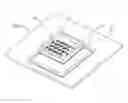
FIG. 1 is an assembled, perspective view of an electrical connector assembly in accordance with a preferred embodiment of the present disclosure;
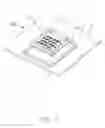
FIG. 2 is an exploded, perspective view of the electrical connector assembly as shown in FIG. 1;
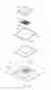
FIG. 3 is an exploded, schematic view of the electrical connector assembly as shown in FIG. 1;
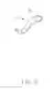
FIG. 4 is a perspective view of a contact as shown in FIG. 1;
FIG. 5 is another view of the contact as shown in FIG. 4.
DETAILED DESCRIPTION OF THE INVENTION
Reference will now be made to the drawings to describe a preferred embodiment of the present disclosure in detail.
Referring to FIGS. 1 and 2, an electrical connector assembly 100 for contacting a package (not show) comprises a printed circuit board (PCB) 6 and an electrical connector assembled on the PCB. The electrical connector comprises an insulating housing 1, a plurality of contacts 2 received in the insulating housing 1 and a metallic stiffener 3 insert molded with the insulating housing 1.
Referring to FIG. 3, the metallic stiffener 3 is rectangular configuration, comprising four side portions 31 successively connecting one and another. The four side portions 31 define a cavity 30 for receiving the insulating housing 1. The stiffener 3 further comprises an outer protrusion 310 extending from the side portion 31 and far away from the cavity 30 and an inner protrusion 311 extending from the side portion 31 and into the cavity 30. In this embodiment, the outer protrusion 310 and the inner protrusion 311 are extending from corner of the metallic stiffener 3. The outer protrusion 310 and the inner protrusion 311 can enlarge the assembling surface and prevent the electrical connector from misassembling when assembling the electrical connector onto the PCB 6.
The insulating housing 1 is insert molding with the stiffener 3 for increasing the strength of the insulating housing 1. The insulating housing 1 locates into the cavity 30. From a top view, the area of the insulating housing is smaller than that of the cavity 30, i.e. the insulating housing 1 locates on partial of the cavity 30. In this embodiment, the insulating housing 1 locates on a corner of the stiffener 3.
Referring to FIGS. 4 and 5, the contact 2 comprises a soldering portion 21 for soldering on the PCB 6 and an elastic arm 22 extending obliquely from the soldering portion 21. The elastic arm 22 comprises a contacting portion 221 for contacting the package. The contact 2 is coated with insulating layer except the contacting portion 221 and a bottom surface of the soldering portion 21. The insulating layer can prevent adjacent contact 2 from electrically connecting with each other and shortened so as to meet fine pitch arrangement requirement.
Referring to FIGS. 2 and 3, the PCB 6 comprises a plurality of pads 60 for contacting the contacts correspondingly. The PCB 6 comprises an alignment feature 61 surrounding the pads 60. The alignment feature 61 comprises a large frame having the same configuration with the frame 3 of the electrical connector. When assembling, just by aligning the stiffener 3 with the alignment feature 61 of the PCB 6 can align the contacts 2 in the insulating housing 1 with the corresponding pads 60 correctly. The alignment feature 61 further comprises a small frame corresponding to the configuration of the insulating housing 1, the insulating housing 1 covers on the small frame. The electrical connector is pasted on the PCB 6. Glue 4 is defined on a bottom surface of the stiffener 3 and periphery of the insulating housing 1. The glue 4 has the same configuration with the alignment feature 61. The stiffener 3 and the insulating housing 1 is pasted upon the alignment feature 61 correspondingly and the contacts 2 connect the pads 60 correspondingly by soldering materials or conducting glue.
While preferred embodiment in accordance with the present disclosure has been shown and described, equivalent modifications and changes known to persons skilled in the art according to the spirit of the present disclosure are considered within the scope of the present disclosure as defined in the appended claims.
Claims
What is claimed is:1. An electrical connector for assembling on a printed circuit board (PCB) having an alignment feature, comprising:
an insulating housing;
a plurality of contacts received in the insulating housing; and
a stiffener insert molding with the insulating housing, the stiffener corresponding to the alignment feature and assembled on the PCB.
2. The electrical connector as claimed in claim 1, wherein the stiffener is a metallic frame while the alignment feature has the same configuration with the metallic frame.
3. The electrical connector as claimed in claim 2, wherein the stiffener defines a cavity, the insulating housing extends into the cavity, and wherein the area of the insulating housing is less than the area of the cavity from a top view.
4. The electrical connector as claimed in claim 3, wherein the stiffener comprises an outer protrusion extending far away from the cavity and an inner protrusion extending into the cavity.
5. The electrical connector as claimed in claim 1, wherein the contact comprises a soldering portion for assembling on the PCB and an elastic arm extending obliquely from the soldering portion, the elastic arm comprises a contacting portion for contacting a package, and wherein the contact is coated with insulating layer except the contacting portion and the soldering portion.
6. The electrical connector as claimed in claim 1, wherein the stiffener is pasted on the PCB.
7. The electrical connector as claimed in claim 1, wherein the contact is soldered on the PCB through soldering materials.
8. The electrical connector as claimed in claim 1, wherein the contact is pasted on the PCB through conducting glue.
9. An electrical connector assembly for contacting a package, comprising:
a printed circuit board (PCB), comprising a plurality of pads and an alignment feature around said a plurality of pads;
an insulating housing having a plurality of contacts retained therein corresponding to said a plurality of pads; and
a stiffener having a plurality of side portions corresponding to the alignment feature of the PCB; wherein
the stiffener and the insulating housing are fixed together, when the side portions of the stiffener is assembled upon the alignment feature correspondingly, the contacts align with the pads of the PCB correspondingly.
10. The electrical connector assembly as claimed in claim 9, wherein the stiffener is a metallic frame formed by four side portions connecting one with another and defining a cavity, the insulating housing extends into the cavity, and wherein the area of the insulating housing is less than the area of the cavity from a top view.
11. The electrical connector assembly as claimed in claim 10, wherein the alignment feature comprises a large frame having the same configuration with the stiffener and a small frame having the same configuration with the insulating housing.
12. The electrical connector assembly as claimed in claim 11, wherein the stiffener and the insulating housing are pasted upon the alignment feature correspondingly.
13. The electrical connector assembly as claimed in claim 9, wherein the stiffener and the insulating housing are insert-molded with each other.
14. The electrical connector assembly as claimed in claim 9, wherein the contact is coated with insulating layer except the portion for contacting the pad of the PCB and the portion for contacting the package.
15. An electrical connector assembly comprising:
a printed circuit board defining on a top surface a first frame structure enclosing a plurality of pads in a top view;
an electrical connector including a second frame structure insert-molded with an insulative housing and attached to the first frame structure in a vertical direction;
a plurality of contacts disposed in the housing and attached, in the vertical direction, to the corresponding pads, respectively.
16. The electrical connector assembly as claimed in claim 15, wherein both said first frame structure and said second frame structure are metallic.
17. The electrical connector assembly as claimed in claim 15, wherein each of the contacts is coated with an insulative layer except around an upper contact section for mating an electronic package upon the housing, and a lower contact section for contacting the corresponding pad.
18. The electrical connector assembly as claimed in claim 15, wherein the first frame structure is dimensioned similar to the second frame structure in the top view.
19. The electrical connector assembly as claimed in claim 15, wherein both said first frame structure and said second frame structure are formed continuously with interruptions thereof.
20. The electrical connector assembly as claimed in claim 15, wherein a glue is applied to an underside of the housing and an underside of the second frame structure to fasten the housing and the second frame structure to the first frame structure.
Images & Drawings included:


Sources:
- United States Patent and Trademark Office - verify current appl. status at the USPTO↗
Similar patent applications:
- » 20080153360
Low profile electrical connector - » 20080261417
Low profile electrical connector - » 20050130494
Low profile electrical connector - » 20070243770
Low profile electrical connector assembly and terminal therefor - » 12080293
Low profile electrical connector - » 20080057795
Low profile electrical connector - » 14994532
Low profile electrical connector - » 12219560
Low-profile electrical connector and device thereof - » 20070117459
Low profile electrical connector - » 20090029567
Low profile electrical connector
Recent applications in this class:
- » 20250219308 2025-07-03
ELECTRICAL CONNECTOR STRUCTURE - » 20250079733 2025-03-06
CABLE CARRIER ADAPTER FOR CONNECTIVITY TO CIRCUIT BOARD AND CONNECTOR - » 20240283175 2024-08-22
CONNECTOR - » 20230318209 2023-10-05
CABLE CONNECTOR AND CONNECTOR ASSEMBLY - » 20230307855 2023-09-28
Connector Device - » 20230187857 2023-06-15
CONNECTOR ASSEMBLY - » 20230126150 2023-04-27
ELECTRICAL CONNECTOR - » 20230106932 2023-04-06
Guide module with integrated connector protection - » 20230040942 2023-02-09
Wire-to-circuit board connection structure and a circuit board-attached cable - » 20220336976 2022-10-20
RECEPTACLE COUPLER FOR COMMUNICATION SYSTEM
Recent applications for this Assignee:
- » 20250218287 2025-07-03
METHOD OF GENERATING AND PROMPTING TRAFFIC INFORMATION, AND ROADSIDE DEVICE THEREOF - » 20250178535 2025-06-05
METHOD FOR CONSTRUCTING 3D PANORAMIC VIEW MODEL, VEHICLE-MOUNTED DEVICE, AND STORAGE MEDIUM - » 20250074444 2025-03-06
METHOD FOR EARLY WARNING A BLIND AREA, ELECTRONIC DEVICE AND STORAGE MEDIUM - » 20240416754 2024-12-19
DISPLAY CONTROL DEVICE, DISPLAY EQUIPMENT, AND VEHICLE EMPLOYING DEVICE - » 20240411051 2024-12-12
Light-emitting device array and optical transceiver system having the same - » 20240324114 2024-09-26
DISPLAY CONTROL DEVICE AND VEHICLE EMPLOYING DEVICE - » 20240295957 2024-09-05
METHOD FOR CONTROLLING ELECTRONIC DEVICE, ELECTRONIC DEVICE AND COMPUTER STROAGE MEDIUM EMPLOYING METHOD - » 20240257357 2024-08-01
METHOD FOR DETECTING OBSTACLES, ELECTRONIC DEVICE, AND STORAGE MEDIUM - » 20240203133 2024-06-20
LANE LINE RECOGNITION METHOD, ELECTRONIC DEVICE AND STORAGE MEDIUM - » 20240194999 2024-06-13
Robot using limiting device for locking battery