Device with a single crystal diamond substrate with a buried electrically conducting layer
US20150223331A1
2015-08-06
14/686,548
2015-04-14
✅ Patent granted
US 9,295,152 B2
2016-03-22
-
-
Thinh T Nguyen
US Naval Research Laboratory | Stephen T. Hunnius
2035-04-14
Abstract:
A device comprising a single crystal diamond substrate with a buried electrically conducting layer with μm square openings spaced apart milled into the diamond by ablating the carbon above wherein the step of ablating uses a diode pumped tripled Nd:YAG laser at 355 nm and wherein the square openings have electrical contacts and wherein the resistance measured between the square openings is dominated by the buried electrically conducting layer and on the order of about 1 kΩ.
Inventors:
- Bradford B. Pate 11 🇺🇸 Arlington, VA, United States
- Jeffrey W. Baldwin 8 🇺🇸 Fairfax, VA, United States
- Matthew P. Ray 2 🇺🇸 Rock Hill, SC, United States
- Matthew P. Ray 1 🇺🇸 Bridal Trail, SC, United States
Assignee:
- The Government of the United States of America, as represented by the Secretary of the Navy 704 🇺🇸 Washington, DC, United States
- The United States of America, as represented by the Secretary of the Navy 4,501 🇺🇸 Washington, DC, United States
Applicant:
Interested in similar patents?
Get notified when new applications in this technology area are published.
Classification:
H05K1/09 » CPC main
Printed circuits; Details Use of materials for the conductive, e.g. metallic pattern
H05K1/09 » CPC main
Printed circuits; Details Use of materials for the conductive, e.g. metallic pattern
B23K26/0622 » CPC further
Working by laser beam, e.g. welding, cutting or boring; Positioning or observing the workpiece, e.g. with respect to the point of impact; Aligning, aiming or focusing the laser beam; Shaping the laser beam, e.g. by masks or multi-focusing by direct control of the laser beam by shaping pulses
B23K26/362 » CPC further
Working by laser beam, e.g. welding, cutting or boring; Removing material Laser etching
B23K26/40 » CPC further
Working by laser beam, e.g. welding, cutting or boring; Removing material taking account of the properties of the material involved
C30B29/04 » CPC further
Single crystals or homogeneous polycrystalline material with defined structure characterised by the material or by their shape; Elements Diamond
C30B33/02 » CPC further
After-treatment of single crystals or homogeneous polycrystalline material with defined structure Heat treatment
H01L29/1608 » CPC further
Semiconductor devices adapted for rectifying, amplifying, oscillating or switching, or capacitors or resistors with at least one potential-jump barrier or surface barrier, e.g. PN junction depletion layer or carrier concentration layer; Details of semiconductor bodies or of electrodes thereof; Multistep manufacturing processes therefor; Semiconductor bodies ; Multistep manufacturing processes therefor characterised by the materials of which they are formed including, apart from doping materials or other impurities, only elements of Group IV of the Periodic System Silicon carbide
H05K3/4602 » CPC further
Apparatus or processes for manufacturing printed circuits; Manufacturing multilayer circuits characterized by a special circuit board as base or central core whereon additional circuit layers are built or additional circuit boards are laminated
H05K3/4602 » CPC further
Apparatus or processes for manufacturing printed circuits; Manufacturing multilayer circuits characterized by a special circuit board as base or central core whereon additional circuit layers are built or additional circuit boards are laminated
H01L23/3732 » CPC further
Details of semiconductor or other solid state devices; Arrangements for cooling, heating, ventilating or temperature compensation ; Temperature sensing arrangements; Selection of materials, or shaping, to facilitate cooling or heating, e.g. heatsinks; Cooling facilitated by selection of materials for the device or materials for thermal expansion adaptation, e.g. carbon Diamonds
H01L29/1602 » CPC further
Semiconductor devices adapted for rectifying, amplifying, oscillating or switching, or capacitors or resistors with at least one potential-jump barrier or surface barrier, e.g. PN junction depletion layer or carrier concentration layer; Details of semiconductor bodies or of electrodes thereof; Multistep manufacturing processes therefor; Semiconductor bodies ; Multistep manufacturing processes therefor characterised by the materials of which they are formed including, apart from doping materials or other impurities, only elements of Group IV of the Periodic System Diamond
H01L2924/00 » CPC further
Indexing scheme for arrangements or methods for connecting or disconnecting semiconductor or solid-state bodies as covered by
H01L2924/0002 » CPC further
Indexing scheme for arrangements or methods for connecting or disconnecting semiconductor or solid-state bodies as covered by; Technical content checked by a classifier Not covered by any one of groups , and
H05K3/0029 » CPC further
Apparatus or processes for manufacturing printed circuits; Working of insulating substrates or insulating layers; Etching of the substrate by chemical or physical means by laser ablation of inorganic insulating material
H05K3/0029 » CPC further
Apparatus or processes for manufacturing printed circuits; Working of insulating substrates or insulating layers; Etching of the substrate by chemical or physical means by laser ablation of inorganic insulating material
H05K2201/0323 » CPC further
Indexing scheme relating to printed circuits covered by; Conductive materials; Materials Carbon
H05K2201/0323 » CPC further
Indexing scheme relating to printed circuits covered by; Conductive materials; Materials Carbon
Y10S438/931 » CPC further
Semiconductor device manufacturing: process Silicon carbide semiconductor
Y10T428/265 » CPC further
Stock material or miscellaneous articles; Web or sheet containing structurally defined element or component, the element or component having a specified physical dimension; Coating layer not in excess of 5 mils thick or equivalent; Up to 3 mils 1 mil or less
Y10T428/30 » CPC further
Stock material or miscellaneous articles Self-sustaining carbon mass or layer with impregnant or other layer
H01L29/15 IPC
Semiconductor devices adapted for rectifying, amplifying, oscillating or switching, or capacitors or resistors with at least one potential-jump barrier or surface barrier, e.g. PN junction depletion layer or carrier concentration layer; Details of semiconductor bodies or of electrodes thereof; Multistep manufacturing processes therefor; Semiconductor bodies ; Multistep manufacturing processes therefor characterised by the materials of which they are formed Structures with periodic or quasi periodic potential variation, e.g. multiple quantum wells, superlattices
H05K3/46 IPC
Apparatus or processes for manufacturing printed circuits Manufacturing multilayer circuits
H05K3/46 IPC
Apparatus or processes for manufacturing printed circuits Manufacturing multilayer circuits
H01L29/16 IPC
Semiconductor devices adapted for rectifying, amplifying, oscillating or switching, or capacitors or resistors with at least one potential-jump barrier or surface barrier, e.g. PN junction depletion layer or carrier concentration layer; Details of semiconductor bodies or of electrodes thereof; Multistep manufacturing processes therefor; Semiconductor bodies ; Multistep manufacturing processes therefor characterised by the materials of which they are formed including, apart from doping materials or other impurities, only elements of Group IV of the Periodic System
B23K26/00 IPC
Working by laser beam, e.g. welding, cutting or boring
B23K26/06 IPC
Working by laser beam, e.g. welding, cutting or boring; Positioning or observing the workpiece, e.g. with respect to the point of impact; Aligning, aiming or focusing the laser beam Shaping the laser beam, e.g. by masks or multi-focusing
B23K26/36 IPC
Working by laser beam, e.g. welding, cutting or boring Removing material
H01L23/373 IPC
Details of semiconductor or other solid state devices; Arrangements for cooling, heating, ventilating or temperature compensation ; Temperature sensing arrangements; Selection of materials, or shaping, to facilitate cooling or heating, e.g. heatsinks Cooling facilitated by selection of materials for the device or materials for thermal expansion adaptation, e.g. carbon
H05K3/00 IPC
Apparatus or processes for manufacturing printed circuits
H05K3/00 IPC
Apparatus or processes for manufacturing printed circuits
Description
REFERENCE TO RELATED APPLICATION
This application is a non-provisional of, and claims priority to and the benefits of, US Provisional Patent Application 61/613,049 filed on Mar. 20, 2012, and U.S. patent application Ser. No. 13/801,495 filed on Mar. 13, 2013, the entireties of each are hereby incorporated by reference.
BACKGROUND
This disclosure provides for a method for a laser ablation technique for electrical contact to a buried electrically conducting layer in diamond. Furthermore this disclosure provides for a device that has a single crystal diamond substrate with a buried electrically conducting layer between two openings formed by the laser ablation technique and having electrical contacts and wherein the resistance measured between the openings is dominated by the buried electrically conducting layer and on the order of about 1 kΩ.
This disclosure demonstrates a facile method to make low-resistance electrical contact to a buried conducting layer in diamond.
Previous methods for establishing contact to a buried, electrically conducting layer in an otherwise insulating diamond have not overcome the obstacles and have do not produced the superior results of the technique disclosed herein.
One example of a previous method is multiple ion implants into diamond (Prins, 1985). This method for establishing electrical contact to the buried implant layer involves performing a series of ion implants over a range of energies to create a damaged diamond region which extends from the surface to the implant layer. Depending on the depth of the buried layer, this method requires many ion implants. Performing many ion implants is a costly and time-consuming procedure requiring highly specialized equipment and skilled personnel to provide maintenance and operation. Furthermore, using the multiple implant method, the electrical contacts to the buried layer must be established before the buried layer is formed by ion implantation.
A second example of a previous method is a laser damage column (Prawer, 1992). This alternative method establishes electrical contact to the buried layer by creating a column of damaged, electrically conducting diamond which extends from the diamond surface to the buried layer using pulsed focused laser irradiation coupled to a conventional microscope with a 50× objective. If the buried layer is slightly opaque, the laser pulse is selectively absorbed in the buried layer. The laser melts the diamond and this melt front propagates to the surface. Upon cooling, highly conductive columns extend from the surface to the buried layer. A disadvantage of this method is that the columns of damaged, electrically conducting material create relatively large contact resistances to the buried layer.
A third example of a previous method is ion implant over gold beads (Olivero, 2009). This alternative is to scan an ion beam along a linear path which terminates at a semi-spherical mask characterized by a non-uniform thickness profile (Au bead made with ball bonder). As the beam scan progresses towards the center of the mask, incident ions cross an increasing thickness of masking material, thus progressively reducing their range in the diamond layer. After removing the mask, the heavily damaged, electrically conducting diamond can be connected with the surface and the implant layer establishing electrical contact. A disadvantage of this method is that irregularities in the semi-spherical mask create discontinuities in the electrically conducting column such that robust electrical contact between the diamond surface and the buried layer is not reliable.
SUMMARY OF DISCLOSURE
Description
This disclosure provides for a method for a laser ablation technique for electrical contact to a buried electrically conducting layer in diamond. Furthermore this disclosure provides for a device that has a single crystal diamond substrate with a buried electrically conducting layer between two openings formed by the laser ablation technique and having electrical contacts and wherein the resistance measured between the openings is dominated by the buried electrically conducting layer and on the order of about 1 kΩ.
Example
Single crystal diamond substrates were prepared by mechanical polishing. A series of treatments to remove contaminants was also performed. This procedure reduces surface roughness to a small fraction of a nanometer, ensuring that the buried layer has a uniform depth and thickness. At room temperature the diamond was implanted, at 7 degrees to the C(100) axis to avoid ion channeling, with a beam of 180 keV followed by 150 keV C+ ions at fluences of 4×10¹⁵ ions/cm2 and 5×10¹⁵ ions/cm2 respectively. During the implant process the near-surface region of the diamond remains relatively undamaged while a thin (˜200 nm), heavily damaged, electrically conducting carbon layer is formed beginning at about 50 nm beneath the diamond surface.
DESCRIPTION OF THE DRAWINGS
The following description and drawings set forth certain illustrative implementations of the disclosure in detail, which are indicative of several exemplary ways in which the various principles of the disclosure may be carried out. The illustrated examples, however, are not exhaustive of the many possible embodiments of the disclosure. Other objects, advantages and novel features of the disclosure will be set forth in the following detailed description when considered in conjunction with the drawings.
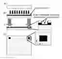
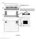
FIG. 1 is a process schematic for fabricating electrical contacts to a buried implant layer in diamond. Part (a) illustrates the polished diamond in cross section; Part (b) illustrates the implant process; Part (c) illustrates the fabrication of electrical contacts. Part (c) shows how the implant layer acts as an ablation stop providing access to the implant layer for electrical contact. Part (d) top view of the diamond showing the fabricated electrical contacts as black squares. The inset in part (d) shows the milled contact pad and the coordinate system used by the laser micro-machining system to raster the sample stage for milling the electrical contacts. Figure is not to scale.
FIG. 2 illustrates an optical micrograph of a milled opening in the diamond skin by laser micro-machining. The milled area provides electrical contact to the buried implant layer as shown in FIG. 2. Ablated material from laser micro-machining is also observed.
FIG. 3 illustrates: a) Surface profilometry of laser ablated electrical contact pad and b) Ion implant damage for (1.5 MeV, C+) as a function of depth using SRIM. The dashed line is a guide for the eye highlighting the agreement between surface profilometry taken over a electrical contact pad fabricated using the laser ablation technique and ion implantation damage as a function of depth simulated with SRIM. This demonstrates that with tuning of the laser parameters, only the diamond above the implant layer is removed.
FIG. 4 illustrates I-V measurements between two contacts composed of: damaged carbon produced by the laser machining process; Cr evaporated over the laser damaged carbon; Cr evaporated over focused ion beam fabricated contacts. The inset shows an I-V measurement taken between a laser machined contact pad capped with Cr and a tungsten point contact on the diamond surface.
DETAILED DESCRIPTION OF THE INVENTION
This disclosure provides for a method for a laser ablation technique for electrical contact to a buried electrically conducting layer in diamond. Furthermore this disclosure provides for a device that has a single crystal diamond substrate with a buried electrically conducting layer between two openings formed by the laser ablation technique and having electrical contacts and wherein the resistance measured between the openings is dominated by the buried electrically conducting layer and on the order of about 1 kΩ.
This disclosure demonstrates a facile method to make low-resistance electrical contact to a buried conducting layer in diamond.
The invention disclosed herein ablates the electrically insulating diamond skin which lies over the electrically conducting buried layer providing access for electrical contact. We use laser micro-machining to open an electrical contact through the diamond skin exposing the buried layer.
Optical transmission microscopy of heavily implanted diamond reveals that the buried layer is opaque so that the laser pulse is primarily absorbed in the implant layer. Machining (laser ablation) of the diamond is performed using a diode pumped, tripled Nd:YAG laser (355 nm) (E-Series Laser Micromachining System, Oxford Lasers Ltd., Didcot, UK.) focused 0.5 mm above the diamond surface. Laser output pulses of 17 μJ are defocused to an ˜9 μm diameter beam spot. The laser pulse duration is nominally 35 ns with a pulse frequency of 10 kHz. Two 300×300 μm square openings spaced 2.45 mm apart are milled into the diamond skin (see FIG. 1).
The milling routine translates the sample stage in a serpentine pattern at a linear speed of 5 mm/sec to mill out the opening (see the inset of FIG. 1 part (d)). Surface profile measurements find that the milled regions are at the same depth as predicted using a simulation after a single pass of the laser (see FIG. 3).
After laser milling, a layer of opaque, electrically conducting, carbon covers the surface of the milled region (FIG. 2) and makes a reliable electrical contact to the conducting buried layer. A robust and facile electrical contact is made by metal evaporation over an area covering, but slightly larger than, the carburized laser-milled regions.
Current-voltage (I-V) measurements (Keithley 2400 SMU) determined the resistance from one contact pad to the other (see FIG. 4), from one contact pad to the diamond surface, and from separated points on the diamond surface. These measurements find linear I-V characteristics between contacts.
In contrast, measurements carried out between similarly separated tungsten point probe contacts on the diamond surface, or between a contact pad and tungsten point probe contact on the diamond surface, show dramatically higher resistance (>2 GΩ) at small applied fields, and non-linear behavior for larger bias voltage (inset of FIG. 4).
The results from the I-V characterization find that the resistance measured between the contact pads is dominated by the electrically conducting buried layer (˜1 kΩ).
Several advantages of this invention are that the contact resistance to the buried layer is reduced. This laser ablation process is a facile, timesaving method to establish electrical contact to a buried, electrically conducting layer over a wide range of depths in an otherwise insulating diamond. For example, removal of 1 μm of diamond (see FIG. 3).
As discussed earlier, multiple ion implants into diamond, laser damage columns, and ion implant over gold beads are previously used methods. However, this invention described herein provides for superior results, for example, reduced contact resistance to the buried layer. Furthermore, this laser ablation process is a facile, timesaving method to establish electrical contact to a buried, electrically conducting layer in an otherwise insulating diamond.
The above examples are merely illustrative of several possible embodiments of various aspects of the present disclosure, wherein equivalent alterations and/or modifications will occur to others skilled in the art upon reading and understanding this specification and the annexed drawings. In addition, although a particular feature of the disclosure may have been illustrated and/or described with respect to only one of several implementations, such feature may be combined with one or more other features of the other implementations as may be desired and advantageous for any given or particular application. Also, to the extent that the terms “including”, “includes”, “having”, “has”, “with”, or variants thereof are used in the detailed description and/or in the claims, such terms are intended to be inclusive in a manner similar to the term “comprising”.
Claims
What we claim is:1. A device comprising:
a single crystal diamond substrate having a first carbon surface;
an electrically conducting carbon layer beneath the first carbon surface formed by implanting the diamond with a beam of 180 KeV followed by 150 KeV C+ ions at fluencies of 4×10¹⁵ ions/cm2 and 5×10¹⁵ ions/cm2 respectively; and
a layer of ablated single crystal diamond wherein the layer lies between the electrically conducting layer and the first carbon surface.
2. The device of claim 1 wherein the layer of ablated single crystal diamond is formed using a diode pumped tripled Nd:YAG laser at 355 nm and wherein the laser pulse duration is about 35 ns with a pulse frequency of 10 kHz.
3. The device of claim 2 wherein the Nd:YAG laser is focused at about 0.5 mm above the first carbon surface.
4. The device of claim 3 wherein the laser is defocused to an about 9 μm diameter beam spot laser output pulses of 17 μJ.
5. The device of claim 4 wherein the implanting occurs at 7 degrees to the C(100) axis;
wherein the electrically conducting carbon layer is about 50 nm beneath the first carbon surface; and
wherein the electrically conducting carbon layer is about 200 nm thick.
6. The device of claim 5 wherein there is no damage at the first carbon surface.
7. The device of claim 6 further including an electrical contact to the electrically conducting carbon layer.
8. A device comprising:
a single crystal diamond substrate with a buried electrically conducting layer with two 300×300 μm square openings spaced about 2.45 mm apart milled into the diamond by ablating the carbon above wherein the step of ablating uses a diode pumped tripled Nd:YAG laser at 355 nm wherein the Nd:YAG laser was focused about 0.5 mm above the first carbon surface the defocusing to an about 9 μm diameter beam spot laser output pulses of 17 μJ wherein the laser pulse duration is about 35 ns with a pulse frequency of 10 kHz and wherein the square openings have electrical contacts and wherein the resistance measured between the square openings is dominated by the buried electrically conducting layer and on the order of about 1 kΩ.
Images & Drawings included:


Sources:
- United States Patent and Trademark Office - verify current appl. status at the USPTO↗
Recent applications in this class:
- » 20250220812 2025-07-03
ANISOTROPIC CONDUCTIVE ELASTIC MATERIAL INCLUDING CONDUCTIVE BALLS AND ITS MANUFACTURING METHOD - » 20250212327 2025-06-26
PRINTED CIRCUIT BOARD - » 20250168977 2025-05-22
Scalable, Printable, Patterned Sheet Of High Mobility Graphene On Flexible Substrates - » 20250142722 2025-05-01
MEMBER FOR FORMING WIRING, METHOD FOR FORMING WIRING LAYER USING MEMBER FOR FORMING WIRING, AND FORMED WIRING MEMBER - » 20250081341 2025-03-06
Method and Apparatus of Conductive Hybrid Material Layer Stacks with Magnetic Material - » 20250056722 2025-02-13
HIGH-INTEGRATION-LEVEL CARRIER PLATE AND MANUFACTURING METHOD - » 20250048550 2025-02-06
TEXTILE CONDUCTIVE BUS AND METHOD OF MAKING THE SAME - » 20250024599 2025-01-16
CERAMIC WIRING MEMBER - » 20250024598 2025-01-16
SUBSTRATE FOR PRINTED WIRING BOARD AND PRINTED WIRING BOARD - » 20240414842 2024-12-12
FLEXIBLE CIRCUIT BOARD
Recent applications for this Assignee:
- » 20240409833 2024-12-12
Sustainable turbine and diesel fuels from isoprene and α olefins - » 20240322426 2024-09-26
Phased Array of Electrolytic Fluid Antennas and a Method for Dynamically Beam Steering the Same - » 20240237991 2024-07-18
Simplified field use junctional tourniquets - » 20240119734 2024-04-11
System and method for efficient filtering, clustering, tracking and persistent motion detection for event cameras - » 20240118137 2024-04-11
Gyro stabilized modular laser measurement device - » 20240069125 2024-02-29
Apparatus and methods for virtually linear and temperature-independent sensing of magnetic fields - » 20240044623 2024-02-08
Fragmentation pattern, optimized for drawn cup warheads with a dome and cylindrical wall - » 20240036295 2024-02-01
Digital Adaptive Optics Encoder Module - » 20230223514 2023-07-13
Fabrication and fusion of zinc particles in porous electrodes - » 20230190301 2023-06-22
Simplified field use junctional tourniquets