Printed wiring board
US20150245482A1
2015-08-27
14/630,048
2015-02-24
✅ Patent granted
US 9,872,388 B2
2018-01-16
-
-
Tuan T Dinh
Hauptman Ham, LLP
2035-04-05
Abstract:
In a printed wiring board on which an electronic component comprising electrode terminal rows on four peripheral sides or two opposite sides thereof is mounted, each of pads at the both ends of pad rows corresponding to the electrode terminal rows extend outwardly relative to the other pads in the direction of arrangement of the pads and has a shape obtained by diagonally cutting a corner located farthest from the center of the electronic component.
Assignee:
- FANUC CORPORATION 3,981 🇯🇵 Yamanashi, Japan
Applicant:
Interested in similar patents?
Get notified when new applications in this technology area are published.
Classification:
H05K1/111 » CPC main
Printed circuits; Details; Printed elements for providing electric connections to or between printed circuits Pads for surface mounting, e.g. lay-out
H05K1/111 » CPC main
Printed circuits; Details; Printed elements for providing electric connections to or between printed circuits Pads for surface mounting, e.g. lay-out
H05K1/181 » CPC further
Printed circuits; Printed circuits structurally associated with non-printed electric components associated with surface mounted components
H05K1/181 » CPC further
Printed circuits; Printed circuits structurally associated with non-printed electric components associated with surface mounted components
H05K1/11 IPC
Printed circuits; Details Printed elements for providing electric connections to or between printed circuits
H05K1/11 IPC
Printed circuits; Details Printed elements for providing electric connections to or between printed circuits
H05K1/18 IPC
Printed circuits Printed circuits structurally associated with non-printed electric components
H05K1/18 IPC
Printed circuits Printed circuits structurally associated with non-printed electric components
H05K3/3421 » CPC further
Apparatus or processes for manufacturing printed circuits; Assembling printed circuits with electric components, e.g. with resistor electrically connecting electric components or wires to printed circuits by soldering; Surface mounted components Leaded components
H05K3/3421 » CPC further
Apparatus or processes for manufacturing printed circuits; Assembling printed circuits with electric components, e.g. with resistor electrically connecting electric components or wires to printed circuits by soldering; Surface mounted components Leaded components
H05K3/3442 » CPC further
Apparatus or processes for manufacturing printed circuits; Assembling printed circuits with electric components, e.g. with resistor electrically connecting electric components or wires to printed circuits by soldering; Surface mounted components; Leadless components having edge contacts, e.g. leadless chip capacitors, chip carriers
H05K7/10 IPC
Constructional details common to different types of electric apparatus; Arrangements of circuit components or wiring on supporting structure Plug-in assemblages of components, e.g. IC sockets
H05K7/10 IPC
Constructional details common to different types of electric apparatus; Arrangements of circuit components or wiring on supporting structure Plug-in assemblages of components, e.g. IC sockets
H05K7/12 IPC
Constructional details common to different types of electric apparatus; Arrangements of circuit components or wiring on supporting structure Resilient or clamping means for holding component to structure
H05K7/12 IPC
Constructional details common to different types of electric apparatus; Arrangements of circuit components or wiring on supporting structure Resilient or clamping means for holding component to structure
H05K3/34 IPC
Apparatus or processes for manufacturing printed circuits; Assembling printed circuits with electric components, e.g. with resistor electrically connecting electric components or wires to printed circuits by soldering
H05K3/34 IPC
Apparatus or processes for manufacturing printed circuits; Assembling printed circuits with electric components, e.g. with resistor electrically connecting electric components or wires to printed circuits by soldering
H05K2201/09381 » CPC further
Indexing scheme relating to printed circuits covered by; Shape and layout; Shape and layout details of conductors; Pads and lands Shape of non-curved single flat metallic pad, land or exposed part thereof; Shape of electrode of leadless component
H05K2201/09381 » CPC further
Indexing scheme relating to printed circuits covered by; Shape and layout; Shape and layout details of conductors; Pads and lands Shape of non-curved single flat metallic pad, land or exposed part thereof; Shape of electrode of leadless component
Description
BACKGROUND OF THE INVENTION
1. Field of the Invention
The present invention relates to a printed wiring board on which electronic components are mounted.
2. Description of the Related Art
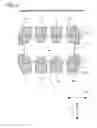
Conventionally, an electronic component 3 is mounted on pads 7 of a printed wiring board 1 in the following manner. As shown in FIG. 6, the rectangular pads 7 are arranged on the printed wiring board 1, depending on the shape, size, layout, etc., of electrode terminals 5 of the electronic component 3. A solder paste is applied to the pads 7 and the electronic component 3 is placed on the paste. The entire structure is heated by a reflow device. The electronic component 3 is mounted on the pads 7 as the solder paste is melted so that the electrode terminals 5 of the electronic component 3 are soldered to the pads 7 of the printed wiring board 1. In FIG. 6, numerals 2, 4 and 6 designate a mounting area, the body, and wiring, respectively. Japanese Patent Application Laid-Open No. 7-183650 relates to this technique.
The conventional technique shown in FIG. 6 has a problem that a large stress is applied to soldered portions of those pads 7 which are located at the both ends of pad rows during a temperature cycle so that surrounding elements are liable to fail due to rupture of the soldered portions.
SUMMARY OF THE INVENTION
Accordingly, the object of the present invention is to provide a printed wiring board configured so that the rupture life of soldered portions of pads thereon can be extended.
According to the present invention, each of pads at the both ends of pad rows that are most heavily stressed during a temperature cycle comprises an extension extending outwardly in the direction of arrangement of the pads from the center of an electronic component, the extension having a shape obtained by diagonally cutting a corner of the pad located farthest from the center of the electronic component.
A printed wiring board according to the present invention is mounted with an electronic component comprising electrode terminal rows on four peripheral sides or two opposite sides thereof. The printed wiring board comprises pad rows corresponding to the electrode terminal rows and each of pads at the both ends of the pad rows comprises an extension extending outwardly relative to the other pads in the direction of arrangement of the pads from the center of the electronic component, the extension having a shape obtained by diagonally cutting a corner located farthest from the center of the electronic component.
Each of the pads at the both ends may have a shape obtained by diagonally cutting the end pad by a segment which connects the points of intersection of two sides between which the corner farthest from the center of the electronic component is located and perpendicular lines extending from the corner to the two sides.
Each of the pads at the both ends may comprise an extension extending outwardly in a direction perpendicular to the direction of arrangement of the pads, as well as in the direction of arrangement of the pads, from the center of the electronic component.
According to the present invention configured as described above, there can be provided a printed wiring board configured so that the rupture life of soldered portions of pads thereon can be extended.
BRIEF DESCRIPTION OF THE DRAWINGS
The above and other objects and features of the present invention will be obvious from the ensuing description of embodiments with reference to the accompanying drawings, in which:
FIG. 1 is a view showing how an electronic component is placed on pads of a printed wiring board;
FIG. 2 is a view showing how outermost pads of FIG. 1 are extended;
FIG. 3 is a view showing how the outermost pads of FIG. 2 are extended and their corners are cut;
FIG. 4 is a view showing how an outermost pad and an electrode terminal of FIG. 2 are soldered to each other;
FIG. 5 is a view showing how an outermost pad and an electrode terminal of FIG. 3 are soldered to each other; and
FIG. 6 is a view showing a conventional technique.
DETAILED DESCRIPTION OF THE PREFERRED EMBODIMENTS
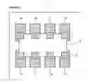
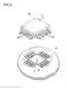
FIG. 1 is a view showing how an electronic component is placed on pads of a printed wiring board. In the present embodiment, each pad is rectangular. A printed wiring board 1 is provided with pads 7 on which an electronic component 3 is mounted. The electronic component 3 is, for example, an electronic component provided with a plurality of electrode terminals 5. Four electrode terminals 5 are arranged side by side on each of two opposite sides of the electronic component 3. In the present embodiment, the electrode terminals 5 are arrayed on four peripheral sides or two opposite sides of the electronic component 3. The electrode terminals 5 of the electronic component 3 and the pads 7 on the printed wiring board 1 are electrically connected and secured to one another by soldering.
FIG. 2 is a view showing how the outermost pads of FIG. 1 are extended. The four outermost ones of the pads (7a, 7b, 7c, 7d, 7e, 7f, 7g and 7h) are designated by 7a, 7d, 7e and 7h, individually. The outermost pads 7a, 7d, 7e and 7h are located individually at the both ends of pad rows corresponding to the rows of the electrode terminals 5 of the electronic component 3.
These pads 7a, 7d, 7e and 7h are extended outwardly relative to the other pads in the direction of their arrangement. Thus, each of the outermost pads has an extension (designated by numeral 8 in FIG. 2), which extends outwardly in the direction of arrangement of the pads from the center of the electronic component.
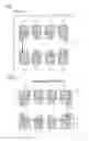
FIG. 3 is a view showing how the outermost pads of FIG. 2 are extended and their corners are cut. “Cutting” here denotes partially removing the pads. Each of the outermost pads 7a, 7d, 7e and 7h has a shape obtained by diagonally cutting a corner or apex portion (see FIG. 2) located farthest from a center 9 of the electronic component 3. Numeral 10 designates a cut portion. A cut line 11 of each of the pads 7a, 7d, 7e and 7h at the both ends is a segment that connects the points of intersection of two sides between which a corner of the electronic component is located and perpendicular lines extending from the corner to the two sides. Further, each of the outermost pads 7a, 7d, 7e and 7h may be extended outwardly in a direction 13 perpendicular to a direction 12 of arrangement of the pads, as well as in the direction 12.
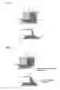
FIG. 4 is a view showing how an outermost pad and an electrode terminal of FIG. 2 are soldered to each other. In FIG. 4, numeral 14 designates a solder fillet. FIG. 5 is a view showing how an outermost pad and an electrode terminal of FIG. 3 are soldered to each other. A larger solder fillet can be formed to improve the resistance to temperature cycling by outwardly extending the pad 7 and increasing the solder supply. As shown in FIG. 5, moreover, the solder fillet can be increased in thickness to also improve the temperature cycling resistance by cutting a corner to prevent extra trailing of the solder fillet.
Claims
1. A printed wiring board on which an electronic component comprising electrode terminal rows on four peripheral sides or two opposite sides thereof is mounted, the printed wiring board comprising:
pad rows corresponding to the electrode terminal rows; and
each of pads at the both ends of the pad rows comprises an extension extending outwardly relative to the other pads in the direction of arrangement of the pads from the center of the electronic component, the extension having a shape obtained by diagonally cutting a corner located farthest from the center of the electronic component.
2. The printed wiring board according to claim 1, wherein each of the pads at the both ends has a shape obtained by diagonally cutting the end pad by a segment which connects the points of intersection of two sides between which the corner of the electronic component is located and perpendicular lines extending from the corner to the two sides.
3. The printed wiring board according to claim 1, wherein each of the pads at the both ends comprises an extension extending outwardly in a direction perpendicular to the direction of arrangement of the pads, as well as in the direction of arrangement of the pads, from the center of the electronic component.
Images & Drawings included:
Sources:
- United States Patent and Trademark Office - verify current appl. status at the USPTO↗
Similar patent applications:
- » 20050014035
Prepreg for printed wiring board, printed wiring board using the prepreg and method for manufacturing the printed wiring board, and multilayer printed wiring board and method for manufacturing the multilayer printed wiring board - » 20220304163
Method for making printed wiring board, printed wiring board, and adhesive film for making printed wiring board - » 20090114432
LAMINATE FOR PRINTED WIRING BOARD, PRINTED WIRING BOARD USING SAME, METHOD FOR MANUFACTURING PRINTED WIRING BOARD, ELECTRICAL COMPONENT, ELECTRONIC COMPONENT, AND ELECTRICAL DEVICE - » 20160007444
Reinforcing member for flexible printed wiring board, flexible printed wiring board, and shield printed wiring board - » 20120037413
Printed wiring board fabrication method, printed wiring board, multilayer printed wiring board, and semiconductor package - » 20160345428
Reinforcing member for flexible printed wiring board flexible printed wiring board, and shield printed wiring board - » 20170327630
RESIN FILM, COVERLAY FOR PRINTED WIRING BOARD, SUBSTRATE FOR PRINTED WIRING BOARD, AND PRINTED WIRING BOARD - » 20250071894
PRINTED WIRING BOARD SUBSTRATE, PRINTED WIRING BOARD, AND MULTILAYER PRINTED WIRING BOARD - » 20210014966
Printed wiring board, multilayer printed wiring board and method for manufacturing printed wiring board - » 20130220685
Copper foil for printed wiring board, method for producing said copper foil, resin substrate for printed wiring board and printed wiring board
Recent applications in this class:
- » 20250240886 2025-07-24
INTERPOSER FOR ACTIVE IMPLANTABLE MEDICAL DEVICE - » 20250227840 2025-07-10
FLEXIBLE PRINTED CIRCUIT BOARD, COF MODULE, AND ELECTRONIC DEVICE COMPRISING THE SAME - » 20250212329 2025-06-26
ELECTRONIC BOARD - » 20250203773 2025-06-19
SEMICONDUCTOR PACKAGE AND METHODS OF FORMATION - » 20250176105 2025-05-29
SELECTIVE TRANSFER OF MICRO DEVICES - » 20250176104 2025-05-29
PRINTED CIRCUIT BOARD AND SEMICONDUCTOR PACKAGE INCLUDING THE SAME - » 20250176103 2025-05-29
PRINTED CIRCUIT BOARD AND MANUFACTURING METHOD THEREOF - » 20250159805 2025-05-15
ELECTRONIC DEVICE - » 20250159804 2025-05-15
PRINTED CIRCUIT BOARD HAVING OPTIONAL CIRCUIT UNIT - » 20250159803 2025-05-15
CIRCUIT BOARD AND METHOD OF FABRICATING CIRCUIT BOARD
Recent applications for this Assignee:
- » 20250258475 2025-08-14
COMPUTATION DEVICE, MACHINE TOOL, MACHINE TOOL CONTROL DEVICE, AND STORAGE MEDIUM - » 20250256398 2025-08-14
ROBOT CONTROL DEVICE, NUMERICAL CONTROL SYSTEM, AND NUMERICAL CONTROL METHOD - » 20250251710 2025-08-07
MOTOR MONITORING DEVICE - » 20250250525 2025-08-07
CELL CULTURE VESSEL AND CELL CULTURE DEVICE - » 20250249608 2025-08-07
WIRE-BODY-MANAGING DEVICE, WIRE-BODY-MANAGING METHOD, AND ROBOT - » 20250229441 2025-07-17
COVERING MEMBER FIXING STRUCTURE, MACHINE, AND ROBOT - » 20250224272 2025-07-10
LASER PATH DISPLAY DEVICE AND STORAGE MEDIUM - » 20250214228 2025-07-03
COUPLING STRUCTURE AND PARALLEL LINK ROBOT - » 20250209646 2025-06-26
INDUSTRIAL SYSTEM CONTROL DEVICE, INDUSTRIAL SYSTEM, AND IMAGE ACQUISITION METHOD - » 20250208601 2025-06-26
INFORMATION PROCESSING DEVICE, MACHINE TOOL CONTROL DEVICE, AND NON-TRANSITORY COMPUTER-READABLE MEDIUM STORING A COMPUTER PROGRAM