Apparatus for supplying gate driving voltages, method therefor and display apparatus
US20150280700A1
2015-10-01
14/375,356
2013-07-19
✅ Patent granted
US 9,899,997 B2
2018-02-20
WO; PCT/CN2013/079714; 20130719
WO; WO2014/183336; 20141120
Kent Chang | Scott Au
Ladas & Parry LLP
2034-01-20
Abstract:
There are provided an apparatus for supplying gate driving voltages, a method for supplying gate driving voltages and a display apparatus to which the apparatus for supplying gate driving voltages is applied to. In the apparatus for supplying gate driving voltages, there is disposed a starting voltage boost module connected with a starting voltage output module. The starting voltage boost module is configured to boost a second preset voltage to a third preset voltage higher than a first preset voltage in advance within a predetermined period of time when the second preset voltage is restored to the first preset voltage. By means of the third preset voltage with a higher voltage, the time taken by a gate ON voltage to be restored to the first preset voltage from the second preset voltage is shortened, a response speed is quicken and a problem of too slow restoration due to a large load is settled, so that a charging time of a liquid crystal display panel is increased and the display quality of the picture is enhanced.
Assignee:
- BEIJING BOE DISPLAY TECHNOLOGY CO., LTD. 1,501 🇨🇳 Beijing, China
- BOE TECHNOLOGY GROUP CO., LTD. 20,350 🇨🇳 Beijing, China
Applicant:
Interested in similar patents?
Get notified when new applications in this technology area are published.
Classification:
G09G3/3648 » CPC further
Control arrangements or circuits, of interest only in connection with visual indicators other than cathode-ray tubes for presentation of an assembly of a number of characters, e.g. a page, by composing the assembly by combination of individual elements arranged in a matrix no fixed position being assigned to or needed to be assigned to the individual characters or partial characters by control of light from an independent source using liquid crystals; Control of matrices with row and column drivers using an active matrix
G09G2300/0871 » CPC further
Aspects of the constitution of display devices; Active matrix structure, i.e. with use of active elements, inclusive of non-linear two terminal elements, in the pixels together with light emitting or modulating elements; Several active elements per pixel in active matrix panels with level shifting
G09G3/36 IPC
Control arrangements or circuits, of interest only in connection with visual indicators other than cathode-ray tubes for presentation of an assembly of a number of characters, e.g. a page, by composing the assembly by combination of individual elements arranged in a matrix no fixed position being assigned to or needed to be assigned to the individual characters or partial characters by control of light from an independent source using liquid crystals
H03K17/0412 IPC
Electronic switching or gating, i.e. not by contact-making and –breaking; Modifications for accelerating switching without feedback from the output circuit to the control circuit by measures taken in the control circuit
H03K17/0812 IPC
Electronic switching or gating, i.e. not by contact-making and –breaking; Modifications for protecting switching circuit against overcurrent or overvoltage without feedback from the output circuit to the control circuit by measures taken in the control circuit
G09G3/3677 » CPC further
Control arrangements or circuits, of interest only in connection with visual indicators other than cathode-ray tubes for presentation of an assembly of a number of characters, e.g. a page, by composing the assembly by combination of individual elements arranged in a matrix no fixed position being assigned to or needed to be assigned to the individual characters or partial characters by control of light from an independent source using liquid crystals; Control of matrices with row and column drivers; Details of drivers for scan electrodes suitable for active matrices only
G09G3/3696 » CPC further
Control arrangements or circuits, of interest only in connection with visual indicators other than cathode-ray tubes for presentation of an assembly of a number of characters, e.g. a page, by composing the assembly by combination of individual elements arranged in a matrix no fixed position being assigned to or needed to be assigned to the individual characters or partial characters by control of light from an independent source using liquid crystals; Control of matrices with row and column drivers Generation of voltages supplied to electrode drivers
H03K17/08122 » CPC further
Electronic switching or gating, i.e. not by contact-making and –breaking; Modifications for protecting switching circuit against overcurrent or overvoltage without feedback from the output circuit to the control circuit by measures taken in the control circuit in field-effect transistor switches
G09G2330/023 » CPC further
Aspects of power supply; Aspects of display protection and defect management; Details of power systems and of start or stop of display operation; Power management, e.g. power saving using energy recovery or conservation
G09G2320/0223 » CPC further
Control of display operating conditions; Improving the quality of display appearance Compensation for problems related to R-C delay and attenuation in electrodes of matrix panels, e.g. in gate electrodes or on-substrate video signal electrodes
H03K17/04123 » CPC main
Electronic switching or gating, i.e. not by contact-making and –breaking; Modifications for accelerating switching without feedback from the output circuit to the control circuit by measures taken in the control circuit in field-effect transistor switches
Description
TECHNICAL FIELD
The present disclosure relates to a field of display technique, and more particularly to an apparatus for supplying gate driving voltages, a method therefor and a display apparatus.
BACKGROUND
A Thin Film Transistor-Liquid Crystal Display (TFT-LCD) has been widely applied to an electronic product such as a TV, a mobile phone, a display, etc, and occupied a dominant position in a tablet panel display field, since it is advantageous in that it can provide stable pictures and lively images, eliminate radicalizations, save space and power consumption, and the like.
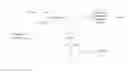
In order to control a switching of the thin film transistor, in general, an apparatus for supplying gate driving voltages supplies a gate ON voltage VON to a gate driving integrated circuit, the gate ON voltage VON is generally between 18 V-30 V and its exact voltage value depends on a specific design of the thin film transistor. A Multi Level Gate (MLG) driving technique is usually utilized to reduce a picture flicker, that is, the gate ON voltage VON is processed by a Multi Level Gate driving integrated circuit (MLG IC). In particular, as shown in FIG. 1: at a specific time, a first preset voltage VGH would drop to a second preset voltage VGH′, wherein the second preset voltage VGH′ is lower than first preset voltage VGH but would not cause the thin film transistor to be turned off yet, so that a chamfered angle might appear in an output waveform of the gate driving integrated circuit, as illustrated in FIG. 2. There is a certain restoration time when the second preset voltage VGH′ is to be restored to the first preset voltage VGH due to a load, e.g., as a restoration time t shown in FIG. 3. A length of the restoration time t would affect a charging time of a liquid crystal display panel, and especially in a product for displaying pictures with a high frame rate, the length of the restoration time t is extremely important since a charging time of a driving thin film transistor is significant insufficient per se.
In conclusion, there is greatly desired an apparatus for supplying gate driving voltages and a method for supplying the gate driving voltages capable of shortening a time taken by the gate ON voltage to be restored to the first preset voltage VGH from the second preset voltage VGB′.
SUMMARY
The present disclosure provides an apparatus for supplying gate driving voltages which is capable of shortening a time taken by the gate ON voltage to be restored to the first preset voltage VGH from the second preset voltage VGH′, so that the charging time of the liquid crystal display panel is prevented from being affected, a response speed is quicken and a display quality of the picture is enhanced. Furthermore, the present disclosure provides a method for supplying the gate driving voltages and a display apparatus to which the apparatus for supplying the gate driving voltages is applied.
Solutions utilized in embodiments of the present disclosure are as follows.
An apparatus for supplying gate driving voltages, comprising:
a starting voltage output module configured to output a gate ON voltage to a gate driving integrated circuit; the gate ON voltage comprises a first preset voltage and a second preset voltage being lower than the first preset voltage;
further comprising:
a starting voltage boost module, connected with the starting voltage output module, configured to boost the second preset voltage to a third preset voltage higher than the first preset voltage within a predetermined period of time when the second preset voltage is to be restored to the first preset voltage.
Optionally, the starting voltage boost module comprises a voltage regulating unit and a switch unit;
the voltage regulating unit is connected with the starting voltage output module and is configured to boost the second preset voltage to the third preset voltage; and
the switch unit is connected with the voltage regulating unit and is configured to turn on or turn off the voltage regulating unit at regular time.
Optionally, the starting voltage output module comprises a charge pump circuit; the charge pump circuit comprises a charge pump, a charge pump adjuster and a reference voltage terminal;
an output terminal of the charge pump is connected with the gate driving integrated circuit and is also connected with the reference voltage terminal via a voltage-dividing resistor;
the reference voltage terminal is further connected with the voltage regulating unit, and is configured to provide a reference voltage; and
the charge pump adjuster is connected with an input terminal of the charge pump, and is configured to control the charge pump to output the gate ON voltage according to the reference voltage and the voltage boosted by the voltage regulating unit.
Optionally, the voltage regulating unit comprises a protective resister and a boost resister connected at the reference voltage terminal in parallel, and the switch unit is disposed on a path between the boost resister and the reference voltage terminal.
Optionally, the voltage regulating unit comprises a protective resister and a boost resister connected at the reference voltage terminal in series, and the switch unit is connected with the boost resister in parallel.
Optionally, the switch unit comprises a switch element and a timing controller connected with the switch element.
Optionally, the switch element is a thin film transistor.
Optionally, the gate driving integrated circuit is a Multi-Level Gate driving integrated circuit.
The embodiments of the present disclosure further provide a method for supplying gate driving voltages, comprising steps of:
outputting a gate ON voltage to a gate driving integrated circuit, wherein the gate ON voltage comprises a first preset voltage and a second preset voltage being lower than the first preset voltage; boosting the second preset voltage to a third preset voltage higher than the first preset voltage within a predetermined period of time when the second preset voltage is to be restored to the first preset voltage.
Optionally, when the second preset voltage is restored to the first preset voltage, a voltage regulating unit is controlled to boost the second preset voltage to the third preset voltage and maintain the same for a predetermined period of time by a control signal applied by a timing controller.
The embodiments of the present disclosure further provide a display apparatus comprising any one of the apparatus for supplying gate driving voltages described above.
By disposing the starting voltage boost module connected with the starting voltage output module, the apparatus for supplying gate driving voltages according to the embodiments of the present disclosure boosts the second preset voltage to the third preset voltage higher than the first preset voltage in advance within the predetermined period of time by the starting voltage boost module when the second preset voltage is restored to the first preset voltage, shortens the time taken by the gate ON voltage to be restored to the first preset voltage from the second preset voltage by means of the third preset voltage with a higher voltage; therefore, the response speed is quicken and a problem of too slow restoration due to a large load is settled, so that the charging time of the liquid crystal display panel is increased and the display quality of the picture is enhanced.
BRIEF DESCRIPTION OF THE DRAWINGS
FIG. 1 is an exemplary waveform diagram of a gate ON voltage as known;
FIG. 2 is an exemplary view illustrating a output waveform of a gate driving integrated circuit as known;
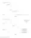
FIG. 3 is an exemplary view illustrating a waveform when a second preset voltage is restored to a first preset voltage as known;
FIG. 4 is an exemplary view illustrating a waveform when the second preset voltage is restored to the first preset voltage according to embodiments of the present disclosure;
FIG. 5 is an exemplary view illustrating a configuration of an apparatus for supplying gate driving voltages according to the embodiments of the present disclosure;
FIG. 6 is an exemplary view illustrating a structure of a detailed implementation of the apparatus for supplying gate driving voltages in FIG. 5; and
FIG. 7 is an exemplary view illustrating a control timing of a method for supplying gate driving voltages according to the embodiments of the present disclosure.
DETAILED DESCRIPTION
Detailed implementations of the present disclosure would be further described below in connection with drawings and embodiments. Following embodiments are only used to explain the present disclosure but not to limit a scope of the present disclosure.
An apparatus for supplying gate driving voltages according to the embodiments of the present disclosure mainly comprises: a starting voltage output module and a starting voltage boost module connected with the starting voltage output module; the starting voltage output module is configured to output a gate ON voltage VON to a gate driving integrated circuit, and the gate driving integrated circuit utilizes a multi level gate driving integrated circuit in order to reduce picture flickers; the gate ON voltage VON comprises a first preset voltage VGH with a modulated chamfered angle and a second preset voltage VGH′ lower than the first preset voltage VGH. As illustrated in FIG. 3, as known, when the gate ON voltage VON is to be restored to the first preset voltage VGH from the second preset voltage VGH′, there would be a certain restoration time t if a load exists, and this time is generally so long that a charge time of a liquid crystal display panel is affected. One main improvement of the present disclosure is in that: the disposed starting voltage boost module boosts the second preset voltage VGH′ to a third preset voltage VGH″ higher than the first preset voltage VGH in advance within a predetermined period of time when the second preset voltage VGH′ is to be restored to the first preset voltage VGH, wherein the third preset voltage VGH″ drops to the first preset voltage VGH after a predetermined period of time lapses; an amplitude and duration of the third preset voltage VGH″ are designed on the basis of the actual requirements so as to achieve an optimum effect. For example, the duration may be shorten properly if the third preset voltage VGH″ is great. As illustrated in FIG. 4, the third preset voltage VGH″ with a higher voltage may shorten the time taken by the gate ON voltage to be restored to the first preset voltage VGH from the second preset voltage. VGH′. It can be seen that, the effect is very notable in a case that the load exists, which can greatly shorten the time taken by the gate ON voltage to be restored to the first preset voltage VGH from the second preset voltage VGE′.
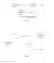
As illustrated in FIG. 5, the starting voltage boost module in the present embodiment comprises a voltage regulating unit and a switch unit; the voltage regulating unit is connected with the starting voltage output module and is configured to boost the second preset voltage VGH′ to the third preset voltage VGH″ higher than the first preset voltage VGH; and the switch unit is connected with the voltage regulating unit and is configured to turn on or turn off the voltage regulating unit at a regular time, so that the third preset voltage VGH″ is maintained for the predetermined period of time, and the voltage regulating unit is turned off after the predetermined period of time, then the gate ON voltage VON is still at the first preset voltage VGH.
Since a charge pump stores energy with a capacitor and has fewer components connected externally, it is very suitable for a portable device; and it is also applicable to an application circuit requiring a large current as its circuit structure is improved and its process level is enhanced continually. Therefore, a charge pump circuit with a high efficiency has been applied in a power management circuit widely due to its advantages of low power consumption, low cost, simply structure, fewer peripheral components and high suppression for electromagnetic interference and the like.
As illustrated in FIG. 6, the starting voltage output module of the present disclosure comprises a charge pump circuit configured to generate the gate ON voltage VON. The charge pump circuit comprises a charge pump, a charge pump adjuster, a voltage-dividing resistor RI and a reference voltage terminal D; an input terminal of the charge pump is connected with an AVDD terminal providing an original power supply, an output terminal of the charge pump is connected with the gate driving integrated circuit and is also connected with the reference voltage terminal D via the voltage-dividing resistor R1; the reference voltage terminal D is further connected with the voltage regulating unit, and is configured to provide a reference voltage VREF; and the charge pump adjuster is disposed in a power management unit (not shown), and is connected with the input terminal of the charge pump, and is configured to control the gate ON voltage VON outputted from the charge pump according to the reference voltage VREF and the voltage boosted by the voltage regulating unit. The voltage regulating unit may be embodied in many implementations. For example, as illustrated in FIG. 6, the voltage regulating unit comprises a protective resister R2 and a boost resister R3 connected in parallel at the reference voltage terminal D, and the switch unit is disposed on a path between the boost resister R3 and the reference voltage terminal D. The gate ON voltage VON is fed back to the power management unit via the voltage-dividing resistor R1 after it is outputted from the charge pump circuit, a feedback output terminal (not shown) of the power management unit provides the fixed reference voltage VREF (normally, 1.25 V) to the reference voltage terminal D; then a pulse width outputted is adjusted by the charge pump adjuster in the power management unit, and in turn the output of the gate ON voltage VON is stabilized. The voltage VON can be calculated as follows.
When the switch unit is turned on:
VON=VREF×(1+R1/(R2//R3)).
When the switch unit is turned off:
VON=VREF×(1+R1/R2).
The outputted gate ON voltage VON when the switch unit is turned on may be greater than that the outputted gate ON voltage VON when the switch unit is turned off, since (R2//R3))<R2.
Herein (R2//R3) represents a resistance when the R2 and R3 are connected in parallel, and the resistance of the (R2//R3) is equal to R2×R3/(R2+R3).
Alternatively, the voltage regulating unit comprises a protective resister R2′ and a boost resister R3′ connected in series at the reference voltage terminal D, and the switch unit is connected with the boost resister R3′ in parallel. The voltage VON can be calculated as follows.
When the switch unit is turned off:
VON=VREF×(1+R1/(R2′+R3′)).
When the switch unit is turned on:
VON=VREF×(1+R1/R2′).
The outputted voltage of the gate ON voltage VON when the switch unit is turned off may be lower than that the outputted gate ON voltage VON when the switch unit is turned on, since (R2′+R3′)>R2′.
As such, the switch unit may be turned on for the predetermined period of time at regular time, and the second preset voltage VGH′ may be boosted to the third preset voltage VGH″ higher than the first preset voltage VGH within the predetermined period of time.
For facilitating the control, the switch unit of the present embodiment comprises a switch element T1 and a timing controller T-CON connected with the switch element T1. Optionally, the switch element is a thin film transistor, and may be an N-type thin film transistor or a P-type thin film transistor, or may be a switch with other type.
The embodiments of the present disclosure further provide a method for supplying gate driving voltages, and as compared with the known method, one of its main improvements is in that: the second preset voltage VGH′ is boosted to the third preset voltage VGH″ higher than the first preset voltage VGH within the predetermined period of time when the second preset voltage VGH′ is to be restored to the first preset voltage VGH, and the third preset voltage VGH″ drops to the first preset voltage VGH after the predetermined period of time lapses. The method for supplying the gate driving voltages will be described in detail below in connection with the above apparatus for supplying the gate driving voltages and FIG. 7.
In an example, when the second preset voltage VGH′ is restored to the first preset voltage VGH, a switch time of a thin film transistor T1 is controlled by a control signal OE3 applied by the timing controller T-CON, such that the voltage regulating unit is controlled to boost the second preset voltage VGH′ to the third preset voltage VGH″ and maintain the latter for the predetermined period of time; therefore, the time taken by the gate ON voltage to be restored to the first preset voltage VVGH from the second preset voltage VGH′ can be shortened by means of the third preset voltage VGH″ with a higher voltage.
Thereafter, the gate ON voltage VON is inputted into the multi level gate driving integrated circuit, and the multi level gate driving integrated circuit may further receive two inputs, one is the second preset voltage VGH′ configured to set a voltage to which the output to be reduced, and the other is a control signal OE2 applied by the timing controller T-CON which is configured to control a timing at which a voltage to be reduced to the second preset voltage VGH′. Thus, the required gate output voltage VOUT may be generated, and the exemplary corresponding waveforms of the gate output voltage VOUT are as shown in FIG. 7.
The embodiments of the present disclosure further provide a display apparatus comprising the apparatus for supplying gate driving voltages described above. Since the applied apparatus for supplying gate driving voltages shortens the time taken by the gate ON voltage VON to be restored to the first preset voltage VGH from the second preset voltage VGH′, the response speed is quicken and a problem of too slow restoration due to a large load is settled, so that the charging time of the liquid crystal display panel is increased and the display quality of the picture is enhanced. This is especially notable in a product for displaying pictures with a high frame rate.
It may understand that above embodiments are only illustrative implementations utilized for explaining the principle of the present disclosure; however, the present disclosure is not limited thereto. For those ordinary skilled in the art, many variations or improvements may be made without departing from the spirit and essence of the present disclosure, and all equivalent solutions also fall into the protection scope of the present disclosure.
Claims
1. An apparatus for supplying gate driving voltages, comprising:
a starting voltage output module configured to output a gate ON voltage to a gate driving integrated circuit; wherein the gate ON voltage comprises a first preset voltage and a second preset voltage being lower than the first preset voltage;
the apparatus further comprising:
a starting voltage boost module, connected with the starting voltage output module, configured to boost the second preset voltage to a third preset voltage higher than the first preset voltage within a predetermined period of time when the second preset voltage is to be restored to the first preset voltage.
2. The apparatus for supplying gate driving voltages of claim 1, wherein the starting voltage boost module comprises a voltage regulating unit and a switch unit;
the voltage regulating unit is connected with the starting voltage output module and is configured to boost the second preset voltage to the third preset voltage; and
the switch unit is connected with the voltage regulating unit and is configured to turn on or turn off the voltage regulating unit at regular time.
3. The apparatus for supplying gate driving voltages of claim 2, wherein the starting voltage output module comprises a charge pump circuit; the charge pump circuit comprises a charge pump, a charge pump adjuster and a reference voltage terminal;
an output terminal of the charge pump is connected with the gate driving integrated circuit and is further connected with the reference voltage terminal via a voltage-dividing resistor;
the reference voltage terminal is further connected with the voltage regulating unit, and is configured to provide a reference voltage; and
the charge pump adjuster is connected with an input terminal of the charge pump, and is configured to control the charge pump to output the gate ON voltage according to the reference voltage and the voltage boosted by the voltage regulating unit.
4. The apparatus for supplying gate driving voltages of claim 3, wherein the voltage regulating unit comprises a protective resister and a boost resister connected at the reference voltage terminal in parallel, and the switch unit is disposed on a path between the boost resister and the reference voltage terminal.
5. The apparatus for supplying gate driving voltages of claim 3, wherein the voltage regulating unit comprises a protective resister and a boost resister connected at the reference voltage terminal in series, and the switch unit is connected with the boost resister in parallel.
6. The apparatus for supplying gate driving voltages of claim 2, wherein the switch unit comprises a switch element and a timing controller connected with the switch element.
7. The apparatus for supplying gate driving voltages of claim 6, wherein the switch element is a thin film transistor.
8. The apparatus for supplying gate driving voltages of claim 1, wherein the gate driving integrated circuit is a Multi Level Gate driving integrated circuit.
9. A method for supplying gate driving voltages, comprising steps of:
outputting a gate ON voltage to a gate driving integrated circuit, wherein the gate ON voltage comprises a first preset voltage and a second preset voltage being lower than the first preset voltage; wherein, the second preset voltage is boosted to a third preset voltage higher than the first preset voltage within a predetermined period of time when the second preset voltage is to be restored to the first preset voltage.
10. The method of claim 9, wherein when the second preset voltage is restored to the first preset voltage, a voltage regulating unit is controlled to boost the second preset voltage to the third preset voltage and maintain the same for a predetermined period of time by a control signal applied by a timing controller.
11. A display apparatus comprising the apparatus for supplying gate driving voltages according to claim 1.
12. The display apparatus of claim 11, wherein the starting voltage boost module comprises a voltage regulating unit and a switch unit;
the voltage regulating unit is connected with the starting voltage output module and is configured to boost the second preset voltage to the third preset voltage; and
the switch unit is connected with the voltage regulating unit and is configured to turn on or turn off the voltage regulating unit at regular time.
13. The display apparatus of claim 12, wherein the starting voltage output module comprises a charge pump circuit; the charge pump circuit comprises a charge pump, a charge pump adjuster and a reference voltage terminal;
an output terminal of the charge pump is connected with the gate driving integrated circuit and is further connected with the reference voltage terminal via a voltage-dividing resistor;
the reference voltage terminal is further connected with the voltage regulating unit, and is configured to provide a reference voltage; and
the charge pump adjuster is connected with an input terminal of the charge pump, and is configured to control the charge pump to output the gate ON voltage according to the reference voltage and the voltage boosted by the voltage regulating unit.
14. The display apparatus of claim 13, wherein the voltage regulating unit comprises a protective resister and a boost resister connected at the reference voltage terminal in parallel, and the switch unit is disposed on a path between the boost resister and the reference voltage terminal.
15. The display apparatus of claim 13, wherein the voltage regulating unit comprises a protective resister and a boost resister connected at the reference voltage terminal in series, and the switch unit is connected with the boost resister in parallel.
16. The display apparatus of claim 12, wherein the switch unit comprises a switch element and a timing controller connected with the switch element.
17. The display apparatus of claim 16, wherein the switch element is a thin film transistor.
18. The display apparatus of claim 11, wherein the gate driving integrated circuit is a Multi Level Gate driving integrated circuit.
Images & Drawings included:

Sources:
- United States Patent and Trademark Office - verify current appl. status at the USPTO↗
Recent applications in this class:
- » 20250247086 2025-07-31
Continuously operating bootstrapped switch - » 20250219631 2025-07-03
VOLTAGE BOOSTED TRANSMITTER WITHOUT A NEGATIVE RAIL - » 20250192766 2025-06-12
Methods and Devices to Improve Switching Time by Bypassing Gate Resistor - » 20250158606 2025-05-15
High-Speed Switch with Accelerated Switching Time - » 20250096786 2025-03-20
AUXILIARY CIRCUIT FOR ESTIMATING MILLER PLATEAU, AND DRIVING CIRCUIT AND POWER CONVERSION SYSTEM INCLUDING THE SAME - » 20250070771 2025-02-27
High-Speed Switch with Accelerated Switching Time - » 20240421810 2024-12-19
ADAPTIVE RINGING CLAMP - » 20240333276 2024-10-03
RADIO FREQUENCY SWITCH AND SWITCH CONTROL CIRCUIT THEREOF - » 20240333275 2024-10-03
Control driver circuit and method for power transistor - » 20240322809 2024-09-26
SEMICONDUCTOR DEVICE AND CONTROL CIRCUIT THEREOF
Recent applications for this Assignee:
- » 20250295022 2025-09-18
QUANTUM DOT COMPOSITION, LIGHT-EMITTING ELEMENT, DISPLAY PANEL AND PREPARATION METHOD THEREOF - » 20250295019 2025-09-18
HEAT DISSIPATION FILM, DISPLAY MODULE AND DISPLAY DEVICE - » 20250294987 2025-09-18
DISPLAY PANEL, DISPLAY DEVICE - » 20250294983 2025-09-18
DISPLAY PANEL AND DISPLAY DEVICE - » 20250292736 2025-09-18
DRIVING CIRCUIT, DRIVING METHOD, DRIVING MODULE AND DISPLAY DEVICE - » 20250291336 2025-09-18
COMPUTER-IMPLEMENTED METHOD, APPARATUS FOR MANAGING PRODUCTION OF ONE OR MORE PRODUCTS, AND COMPUTER-PROGRAM PRODUCT - » 20250291215 2025-09-18
CIRCUIT BOARD AND METHOD FOR MANUFACTURING THE SAME, LIGHT-EMITTING SUBSTRATE, BACKLIGHT MODULE, DISPLAY PANEL AND DISPLAY APPARATUS - » 20250287801 2025-09-11
ARRAY SUBSTRATE AND DISPLAY APPARATUS - » 20250287695 2025-09-11
ARRAY PANEL, METHOD OF MANUFACTURING THE SAME AND DISPLAY DEVICE - » 20250287695 2025-09-11
ARRAY PANEL, METHOD OF MANUFACTURING THE SAME AND DISPLAY DEVICE