Double-sided patterned transparent conductive film and method for manufacturing the same
US20150289370A1
2015-10-08
14/000,186
2012-12-20
✅ Patent granted
US 9,532,449 B2
2016-12-27
WO; PCT/CN2012/087076; 20121220
WO; WO2013/166839; 20131114
Ishwarbhai B Patel
James F. Hann | Haynes Beffel & Wolfeld LLP
2034-06-26
Abstract:
A double-sided patterned transparent conductive film includes an upper surface conductive layer (12) and a lower surface conductive layer (12). The upper surface conductive layer is a patterned trench network; the lower surface conductive layer is a full-surface trench network. A trench of the upper surface conductive layer is filled with conductive material (13), and a trench of the lower surface conductive layer is intermittently filled with conductive material (13). The double-sided patterned transparent conductive film has a high resolution, transmittance, independently adjustable square resistance and many other advantages, such that the transparent conductive film saves a cost of PET. According to the manufacturing method, the alignment is not needed for double-sided imprinting of a single flexible substrate, thus the process is simple, low cost, advantageous for industrial production.
Inventors:
- Yulong Gao 12 🇨🇳 Nanchang, China
- Zheng Cui 5 🇨🇳 Suzhou, China
- Hongwei Kang 2 🇨🇳 Nanchang, China
Assignee:
- NANCHANG O-FILM TECH. CO., LTD. 15 🇨🇳 Nanchang, China
Applicant:
Interested in similar patents?
Get notified when new applications in this technology area are published.
Classification:
H05K1/02 IPC
Printed circuits Details
H05K1/02 IPC
Printed circuits Details
H05K1/0274 » CPC further
Printed circuits; Details Optical details, e.g. printed circuits comprising integral optical means
H05K1/0274 » CPC further
Printed circuits; Details Optical details, e.g. printed circuits comprising integral optical means
H05K3/107 » CPC further
Apparatus or processes for manufacturing printed circuits in which conductive material is applied to the insulating support in such a manner as to form the desired conductive pattern by filling grooves in the support with conductive material
H05K3/107 » CPC further
Apparatus or processes for manufacturing printed circuits in which conductive material is applied to the insulating support in such a manner as to form the desired conductive pattern by filling grooves in the support with conductive material
H05K2201/0108 » CPC further
Indexing scheme relating to printed circuits covered by; Dielectrics; Properties and characteristics in general Transparent
H05K2201/0108 » CPC further
Indexing scheme relating to printed circuits covered by; Dielectrics; Properties and characteristics in general Transparent
H05K2201/09036 » CPC further
Indexing scheme relating to printed circuits covered by; Shape and layout; Substrate related Recesses or grooves in insulating substrate
H05K2201/09036 » CPC further
Indexing scheme relating to printed circuits covered by; Shape and layout; Substrate related Recesses or grooves in insulating substrate
H05K1/11 » CPC main
Printed circuits; Details Printed elements for providing electric connections to or between printed circuits
H05K1/11 » CPC main
Printed circuits; Details Printed elements for providing electric connections to or between printed circuits
H05K3/10 IPC
Apparatus or processes for manufacturing printed circuits in which conductive material is applied to the insulating support in such a manner as to form the desired conductive pattern
H05K3/10 IPC
Apparatus or processes for manufacturing printed circuits in which conductive material is applied to the insulating support in such a manner as to form the desired conductive pattern
H01L31/022466 » CPC further
Semiconductor devices sensitive to infra-red radiation, light, electromagnetic radiation of shorter wavelength or corpuscular radiation and specially adapted either for the conversion of the energy of such radiation into electrical energy or for the control of electrical energy by such radiation; Processes or apparatus specially adapted for the manufacture or treatment thereof or of parts thereof; Details thereof; Details; Electrodes made of transparent conductive layers, e.g. TCO, ITO layers
H01L31/1884 » CPC further
Semiconductor devices sensitive to infra-red radiation, light, electromagnetic radiation of shorter wavelength or corpuscular radiation and specially adapted either for the conversion of the energy of such radiation into electrical energy or for the control of electrical energy by such radiation; Processes or apparatus specially adapted for the manufacture or treatment thereof or of parts thereof; Details thereof; Processes or apparatus specially adapted for the manufacture or treatment of these devices or of parts thereof Manufacture of transparent electrodes, e.g. TCO, ITO
H05K3/1258 » CPC further
Apparatus or processes for manufacturing printed circuits in which conductive material is applied to the insulating support in such a manner as to form the desired conductive pattern using printing techniques to apply the conductive material by using a substrate provided with a shape pattern, e.g. grooves, banks, resist pattern
H05K1/092 » CPC further
Printed circuits; Details; Use of materials for the conductive, e.g. metallic pattern Dispersed materials, e.g. conductive pastes or inks
H05K1/092 » CPC further
Printed circuits; Details; Use of materials for the conductive, e.g. metallic pattern Dispersed materials, e.g. conductive pastes or inks
H05K2201/09681 » CPC further
Indexing scheme relating to printed circuits covered by; Shape and layout; Shape and layout details of conductors covering at least two types of conductors provided for in - Mesh conductors, e.g. as a ground plane
H05K2201/09681 » CPC further
Indexing scheme relating to printed circuits covered by; Shape and layout; Shape and layout details of conductors covering at least two types of conductors provided for in - Mesh conductors, e.g. as a ground plane
H05K2203/0514 » CPC further
Indexing scheme relating to apparatus or processes for manufacturing printed circuits covered by; Patterning and lithography; Masks; Details of resist; Patterning and lithography Photodevelopable thick film, e.g. conductive or insulating paste
H05K2203/0514 » CPC further
Indexing scheme relating to apparatus or processes for manufacturing printed circuits covered by; Patterning and lithography; Masks; Details of resist; Patterning and lithography Photodevelopable thick film, e.g. conductive or insulating paste
H05K2203/0545 » CPC further
Indexing scheme relating to apparatus or processes for manufacturing printed circuits covered by; Patterning and lithography; Masks; Details of resist; Patterning and lithography Pattern for applying drops or paste; Applying a pattern made of drops or paste
H05K2203/0545 » CPC further
Indexing scheme relating to apparatus or processes for manufacturing printed circuits covered by; Patterning and lithography; Masks; Details of resist; Patterning and lithography Pattern for applying drops or paste; Applying a pattern made of drops or paste
Y02E10/50 » CPC further
Energy generation through renewable energy sources Photovoltaic [PV] energy
Y02E10/50 » CPC further
Energy generation through renewable energy sources Photovoltaic [PV] energy
Y10T29/49155 » CPC further
Metal working; Method of mechanical manufacture; Electrical device making; Conductor or circuit manufacturing; On flat or curved insulated base, e.g., printed circuit, etc. Manufacturing circuit on or in base
H01L31/0224 IPC
Semiconductor devices sensitive to infra-red radiation, light, electromagnetic radiation of shorter wavelength or corpuscular radiation and specially adapted either for the conversion of the energy of such radiation into electrical energy or for the control of electrical energy by such radiation; Processes or apparatus specially adapted for the manufacture or treatment thereof or of parts thereof; Details thereof; Details Electrodes
H01L31/18 IPC
Semiconductor devices sensitive to infra-red radiation, light, electromagnetic radiation of shorter wavelength or corpuscular radiation and specially adapted either for the conversion of the energy of such radiation into electrical energy or for the control of electrical energy by such radiation; Processes or apparatus specially adapted for the manufacture or treatment thereof or of parts thereof; Details thereof Processes or apparatus specially adapted for the manufacture or treatment of these devices or of parts thereof
H05K3/06 » CPC further
Apparatus or processes for manufacturing printed circuits in which the conductive material is applied to the surface of the insulating support and is thereafter removed from such areas of the surface which are not intended for current conducting or shielding the conductive material being removed chemically or electrolytically, e.g. by photo-etch process
H05K3/12 IPC
Apparatus or processes for manufacturing printed circuits in which conductive material is applied to the insulating support in such a manner as to form the desired conductive pattern using printing techniques to apply the conductive material
H05K3/12 IPC
Apparatus or processes for manufacturing printed circuits in which conductive material is applied to the insulating support in such a manner as to form the desired conductive pattern using printing techniques to apply the conductive material
H05K1/09 IPC
Printed circuits; Details Use of materials for the conductive, e.g. metallic pattern
H05K1/09 IPC
Printed circuits; Details Use of materials for the conductive, e.g. metallic pattern
Description
FIELD OF THE INVENTION
The present invention relates to transparent conductive film and preparation techniques, and more particularly relates to a double-sided patterned transparent conductive film and a manufacturing method thereof.
BACKGROUND OF THE INVENTION
The transparent conductive film is a sheet having a good electrical conductivity and a high transmittance in the visible light. Currently, the transparent conducting films have been widely used in the fields such as flat panel displays, photovoltaic devices, touch panels, and electromagnetic shielding, thus having a very broad market space.
ITO has dominated the market of the transparent conductive film. In most practical applications, such as touch screens, the former often requires exposure, imaging, etching and cleaning processes to pattern the transparent conductive film before use. Comparing to that, using a printing method or a silver salt method to form a metal grids directly on the specified region of the substrate can omit the patterning process, thus it has some advantages such as low pollution, low cost, etc. The patterned flexible transparent conductive films with excellent performance have been acquired using printing method by Japanese companies Dai Nippon Printing, Fujifilm and Gunze, as well as German company PolyIC. Among them, the film obtained by PolyIC has a graphics resolution of 15 μm, a surface square resistance of 0.4-1 Ω/sq, and a light transmittance exceeding 80%.
A transparent conductive film based on embedded patterned metal grid is disclosed, and the transparent conductive film with a PET substrate has a transmittance exceeding 87%; the transparent conductive film with a glass substrate has a transmittance exceeding 90%, and a surface square resistance less than 10 Ω/sq; especially for those having a resolution of metal lines less than 3 μm. However, in order to further reduce costs and make the touch module thinner, many touch screen manufacturers currently has pay more attention on the development of double-sided patterned transparent conductive film.
The trenches of the conventional embedded patterned transparent conductive film are formed by imprint techniques. Therefore, in order to prepare the double-sided patterned transparent conductive film, it is essential to develop a large format roll-to-roll double-sided aligned imprint technique, which, however, is currently far from mature.
Therefore, it is desire to provide a double-sided patterned transparent conductive film which can avoid alignment problems caused by double-sided imprinting.
SUMMARY OF THE INVENTION
In one aspect of the present invention, a double-sided patterned transparent conductive film and a manufacturing method thereof are provided to solve the technical problem in the prior art that roll-to-roll imprinting process requires two-sided alignment.
The technical solution of the present invention is achieved by the following embodiments.
A double-sided patterned transparent conductive film includes an upper surface conductive layer and a lower surface conductive layer. The upper surface conductive layer is a patterned trench network; the lower surface conductive layer is a full-surface trench network. A trench of the upper surface conductive layer is filled with conductive material, and a trench of the lower surface conductive layer is intermittently filled with conductive material.
In addition, the trench network is a trench combination using a polygon trench as a basic unit, wherein a shape of the basic unit is selected from the group consisting of square, rectangular, round, regular hexagonal, regular triangle, and a combination thereof.
In a preferred embodiment, the conductive material intermittently filled in the trench of the lower surface conductive layer appears intermittently in the trench of the lower surface conductive layer by patterning technology.
In a preferred embodiment, the trench network of the upper surface conductive layer of the double-sided patterned transparent conductive film has at least two network densities.
In a preferred embodiment, at least one network of the network densities has a relative transmittance exceeding 90%; at least one network has a relative transmittance less than 80%.
In a preferred embodiment, a relative transmittance of the trench network of the lower surface conductive layer of the double-sided patterned transparent conductive film exceeds 90%.
A method of manufacturing a double-sided patterned transparent conductive film includes the following steps:
step one, defining a patterned trench network on an upper surface of a intermediate layer by imprint technique;
step two, defining a full-surface trench network on a lower surface of the intermediate layer by imprint technique;
step three, filling conductive material in the trenches on the upper surface and the lower surface of a intermediate layer, respectively; and
step four, patterning the unpatterned trench network of the lower surface filled with conductive material according to an alignment mark on the upper surface.
In a preferred embodiment, the imprint technique is hot imprint or UV imprint.
In a preferred embodiment, the alignment mark on the upper surface is an area of the upper surface having a larger network density, which serves as the alignment mark for the patterning the trench network of the lower surface; at least one network of the network density has a relative transmittance exceeding 90%, and at least one network has a relative transmittance less than 80%.
In a preferred embodiment, the patterning of the unpatterned trench network of the lower surface filled with conductive material includes: attaching a negative dry film to the lower surface; aligning the alignment mark on the upper surface with an alignment mark of a photosensitive film; exposing the negative dry film by UV; developing the negative dry film in a developer, such that the exposed area is preserved during the developing process and the unexposed area is removed, the covered conductive material is exposed;
immersing the double-sided transparent conductive film in an etching solution for the conductive material to remove the exposed conductive material; and immersing the double-sided transparent conductive film in a remover to remove the negative dry film and to expose the conductive layer.
In a preferred embodiment, the conductive material is filled by scrape coating or inkjet printing.
Advantageous Effects
(1) The double-sided patterned transparent conductive film according to the present invention has a high resolution, transmittance, independently adjustable square resistance and many other advantages, such that the transparent conductive film saves a cost of PET.
(2) According to the manufacturing method, the alignment is not needed for double-sided imprinting of a single flexible substrate, thus the process is simple, low cost, advantageous for industrial production.
BRIEF DESCRIPTION OF THE DRAWINGS
The components in the drawings are not necessarily drawn to scale, the emphasis instead being placed upon clearly illustrating the principles of the present invention. It should be understood that the invention is not intended to be limited to the precise arrangements and instrumentalities shown.
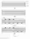
FIG. 1 is a schematic view of a double-sided patterned transparent conductive film according to the present invention;
FIG. 2 is a schematic view showing the patterning process of the lower surface of the double-sided patterned transparent conductive film according to the present invention.
DETAILED DESCRIPTION
The invention will be described in further detail below in conjunction with the drawing. It will be appreciated by those skilled in the art, though, that various changes and modifications can be made without departing from the invention.
Embodiment One
Referring to FIG. 2(F), an embodiment of a double-sided patterned transparent conductive film includes an upper surface conductive layer and a lower surface conductive layer, the upper surface conductive layer of the double-sided patterned transparent conductive film is a patterned trench network, and the lower surface conductive layer is a full-surface trench network. A trench of the upper surface conductive layer is filled with conductive material, and a trench of the lower surface conductive layer is intermittently filled with conductive material.
The trench network of the upper surface conductive layer of the double-sided patterned transparent conductive film has two network densities, one network has a relative transmittance of 90%; the other network has a relative transmittance of 80%. A relative transmittance of the trench network of the lower surface conductive layer of the double-sided patterned transparent conductive film is 90%.
Referring to FIG. 1(A), a UV imprint adhesive 12 is coated on the two surface of the substrate PET 11. Two surfaces of the PET 11 are configured with tackifier layer or dealt with tackifier and the PET 11 has a thickness of 125 μm. The UV imprint adhesive 12, which is H450 Tex, has a thickness of 4 μm. Referring to FIG. 1(B), a patterned trench network is defined on an upper surface 12 by imprint technology; a full-surface unpatterned trench network is defined on a lower surface 12 with a trench depth of 2 μm and a width of 2 μm. Referring to FIG. 1(C), the nano-silver ink is filled in the trenches on the upper surface and the lower surface by scrape coating and then is sintered. The solid content of the silver ink is 35%. The sintering temperature is 135° C. Referring to FIG. 1(D), according to an alignment mark on the upper surface, the silver in the trench network of the lower surface is patterned.
The patterning technology of the lower surface is a very mature technology in the art, which will not be described in details. The following is described as an example.
Referring to FIG. 2(A), the lower surface is a full-surface trench network filled with conductive material; the upper surface is a patterned trench network filled with conductive material.
Referring to FIG. 2(B), a negative dry film 21, which is DuPont1505, is attached to the lower surface. Referring to FIG. 2(C), the alignment mark on the upper surface is aligned with an alignment mark of a photosensitive film 23, and the negative dry film 21 is then exposed by ultraviolet light. Referring to FIG. 2(D), the exposed area is preserved during the developing process while the unexposed area is removed, thus the silver covered by the negative dry film 21 is exposed. The developer is Na2CO3 solution with a mass percentage of 1%. Referring FIG. 2(E), the double-sided transparent conductive film is immersed in a silver etching solution to remove the exposed silver. Referring to FIG. 2(F), the double-sided transparent conductive film is immersed in a remover to remove the negative dry film and to expose the protected silver. The remover is Na2CO3 solution with a mass percentage of 2%.
The intermediate layer of the double-sided transparent conductive film of Embodiment One is not limited to the materials described above, it may be glass, quartz, polymethyl methacrylate (PMMA), polycarbonate (PC), etc. The patterning technology of the lower surface is no limited to the process described above; other technology can be implemented as long as it can pattern the lower surface. The imprint technique may include hot imprint or UV imprint. The conductive material may be filled by scrape coating or inkjet printing. The conductive material of the present invention is not limited to silver, e.g. it may be graphite, polymer conductive materials, and the like.
Although the invention has been described in language specific to structural features and/or methodological acts, it is to be understood that the invention defined in the appended claims is not necessarily limited to the specific features or acts described. Rather, the specific features and acts are disclosed as sample forms of implementing the claimed invention.
Claims
What is claimed is:1. A double-sided patterned transparent conductive film, comprising:
an upper surface conductive layer being a patterned trench network; and
a lower surface conductive layer being a full-surface trench network;
wherein a trench of the upper surface conductive layer is filled with conductive material, and a trench of the lower surface conductive layer is intermittently filled with conductive material.
2. The double-sided patterned transparent conductive film according to claim 1, wherein the conductive material intermittently filled in the trench of the lower surface conductive layer appears intermittently in the trench of the lower surface conductive layer by patterning technology.
3. The double-sided patterned transparent conductive film according to claim 1, wherein the trench network of the upper surface conductive layer of the double-sided patterned transparent conductive film has at least two network densities.
4. The double-sided patterned transparent conductive film according to claim 3, wherein at least one network of the network densities has a relative transmittance exceeding 90%; at least one network has a relative transmittance less than 80%.
5. The double-sided patterned transparent conductive film according to claim 1 or claim 4, wherein a relative transmittance of the trench network of the lower surface conductive layer of the double-sided patterned transparent conductive film exceeds 90%.
6. A method of manufacturing a double-sided patterned transparent conductive film, comprising the following steps:
step one, defining a patterned trench network on an upper surface of a intermediate layer by imprint technique;
step two, defining a full-surface trench network on a lower surface of the intermediate layer by imprint technique;
step three, filling conductive material in the trenches on the upper surface and the lower surface of a intermediate layer, respectively; and
step four, patterning the unpatterned trench network of the lower surface filled with conductive material according to an alignment mark on the upper surface.
7. The method according to claim 6, wherein the imprint technique is hot imprint or UV imprint.
8. The method according to claim 6, wherein the alignment mark on the upper surface is an area of the upper surface having a larger network density, which serves as the alignment mark for the patterning the trench network of the lower surface; at least one network of the network density has a relative transmittance exceeding 90%, and at least one network has a relative transmittance less than 80%.
9. The method according to claim 6, wherein the patterning of the unpatterned trench network of the lower surface filled with conductive material comprises:
attaching a negative dry film to the lower surface;
aligning the alignment mark on the upper surface with an alignment mark of a photosensitive film;
exposing the negative dry film by UV;
developing the negative dry film in a developer, such that the exposed area is preserved during the developing process and the unexposed area is removed, the covered conductive material is exposed;
immersing the double-sided transparent conductive film in an etching solution for the conductive material to remove the exposed conductive material; and
immersing the double-sided transparent conductive film in a remover to remove the negative dry film and to expose the conductive layer.
10. The method according to claim 6 or claim 7, wherein the conductive material is filled by scrape coating or inkjet printing.
Images & Drawings included:

Sources:
- United States Patent and Trademark Office - verify current appl. status at the USPTO↗
Recent applications in this class:
- » 20250287500 2025-09-11
Electrically Conducting Structure for Flexible Circuit Board - » 20250254793 2025-08-07
SYSTEMS, METHODS, STORAGE MEDIUM FOR INKJET-PRINTED GEL-ELECTRONIC - » 20250247955 2025-07-31
SUBSTRATE FOR IMAGE SENSOR - » 20250220814 2025-07-03
MULTILAYER PRINTED CIRCUIT BOARD FOR INTERCONNECTING PIN(S) AND SEMICONDUCTOR DIE(S) AND CORRESPONDING METHOD FOR INTERCONNECTION - » 20250212328 2025-06-26
WIRING CIRCUIT BOARD AND METHOD OF PRODUCING THE WIRING CIRCUIT BOARD - » 20250203772 2025-06-19
TRANSPARENT PACKAGE FOR USE WITH PRINTED CIRCUIT BOARDS - » 20250185164 2025-06-05
MEMBER FOR INTERCONNECTING ELECTRICALLY A PRINTED CIRCUIT BOARD AND AT LEAST ONE PIECE OF ELECTRICAL EQUIPMENT, AND CONNECTING METHOD - » 20250176102 2025-05-29
LOAD REDUCED MEMORY MODULE - » 20250168978 2025-05-22
ELECTRONIC COMPONENT - » 20250159802 2025-05-15
PRINTED CIRCUIT BOARD AND MANUFACTURING METHOD THEREOF
Recent applications for this Assignee:
- » 20170090674 2017-03-30
TOUCH DISPLAY DEVICE - » 20140373776 2014-12-25
Apparatus for substrate double-surface hole-filling - » 20140356584 2014-12-04
TRANSPARENT CONDUCTIVE FILM - » 20140356582 2014-12-04
Single-layer multi-point touch-control conductive film - » 20140353013 2014-12-04
Transparent conductive film - » 20140353011 2014-12-04
Flexible circuit connecting device - » 20140353009 2014-12-04
Transparent conductive film - » 20140353003 2014-12-04
TOUCH-SCREEN CONDUCTIVE FILM AND MANUFACTURING METHOD THEREOF - » 20140293152 2014-10-02
Capacitive touch screen - » 20140293151 2014-10-02
Touch Panel and Manufacturing Method Thereof