Resistor attenuator with switch distortion cancellation
US20160079949A1
2016-03-17
14/857,815
2015-09-17
✅ Patent granted
US 9,813,040 B2
2017-11-07
-
-
Stephen E Jones
Andrew Viger | Charles A. Brill | Frank D. Cimino
2035-09-17
Abstract:
A programmable (multistep) resistor attenuator includes distortion cancellation for harmonic distortion currents. The attenuator includes at last one attenuation stage coupled between a signal input node and a virtual ground node (such as an input to a differential amplifier). The attenuation node is: (a) coupled to the input node through a resistor R; (b) coupled to the virtual ground node through a resistor kR and a virtual ground switch Swf with an on resistance Rswf; and (c) coupled to a differential ground through a resistor mR and a differential ground switch Swp with an on resistance Rswp. Swp is sized relative to Swf such that, when both Swp and Swf are conducting, a component Ipnf of a current Ipn through Rswp and mR to the attenuation node and branching into kR and Rswf, matches, in phase and magnitude, a harmonic current Ifn from the virtual ground through Rswf and kR to the attenuation node, thereby substantially canceling the harmonic distortion appearing at the virtual ground. Distortion cancellation can be based on cancellation is based on matching switches Swf and Swp and the resistors R, mR, kR, and hence is insensitive to PVT variations, input frequency and amplitude. an optimum ratio of Rswp and Rswf is a function of only a ratio of resistors, and hence is insensitive to values of Rswp and Rswf. The attenuator architecture is extendable to multistage configurations.
Assignee:
- TEXAS INSTRUMENTS INCORPORATED 18,931 🇺🇸 Dallas, TX, United States
Applicant:
Interested in similar patents?
Get notified when new applications in this technology area are published.
Classification:
H03F1/56 » CPC further
Details of amplifiers with only discharge tubes, only semiconductor devices or only unspecified devices as amplifying elements Modifications of input or output impedances, not otherwise provided for
H03F3/45 » CPC further
Amplifiers with only discharge tubes or only semiconductor devices as amplifying elements Differential amplifiers
H03F2203/45151 » CPC further
Indexing scheme relating to amplifiers with only discharge tubes or only semiconductor devices as amplifying elements covered by; Indexing scheme relating to differential amplifiers At least one resistor being added at the input of a dif amp
H03H7/24 » CPC main
Multiple-port networks comprising only passive electrical elements as network components Frequency- independent attenuators
H03F1/3211 » CPC further
Details of amplifiers with only discharge tubes, only semiconductor devices or only unspecified devices as amplifying elements; Modifications of amplifiers to reduce non-linear distortion in differential amplifiers
H03F1/32 IPC
Details of amplifiers with only discharge tubes, only semiconductor devices or only unspecified devices as amplifying elements Modifications of amplifiers to reduce non-linear distortion
H03F3/45475 » CPC further
Amplifiers with only discharge tubes or only semiconductor devices as amplifying elements; Differential amplifiers with semiconductor devices only characterised by the way of implementation of the active amplifying circuit in the differential amplifier using IC blocks as the active amplifying circuit
H03F2203/45614 » CPC further
Indexing scheme relating to amplifiers with only discharge tubes or only semiconductor devices as amplifying elements covered by; Indexing scheme relating to differential amplifiers the IC comprising two cross coupled switches
H03F2203/45616 » CPC further
Indexing scheme relating to amplifiers with only discharge tubes or only semiconductor devices as amplifying elements covered by; Indexing scheme relating to differential amplifiers the IC comprising more than one switch, which are not cross coupled
H01P1/22 » CPC further
Auxiliary devices Attenuating devices
H03F2203/45594 » CPC further
Indexing scheme relating to amplifiers with only discharge tubes or only semiconductor devices as amplifying elements covered by; Indexing scheme relating to differential amplifiers the IC comprising one or more resistors, which are not biasing resistor
Description
CROSS-REFERENCE TO RELATED APPLICATIONS
This application claims priority from Indian Provisional Patent Application No. 4523/CHE/2014 (TI-75375PS), filed Sep. 17, 2014, which is hereby incorporated by reference for all purposes.
BACKGROUND
1. Technical Field
This Patent Disclosure relates generally to multistep resistor attenuators, such as for use as a front-end signal attenuator.
2. Related Art
A multistep programmable resistor attenuator is configured from resistors and transistor switches, with transistor switching controlled to provide programmable step attenuation. The switches control current flow, and when on (conducting) are characterized by an Ron resistance.
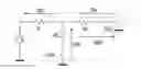
FIG. 1 illustrates a current mode programmable resistor step attenuator, configured as a front-end signal attenuator for a differential amplifier. Signal current flows either to differential ground through the differential switches, or to the virtual grounds at the differential non-inverting and inverting inputs VGP,VGM. For example, a 6 dB step attenuator can be configured with Ra=Rs/2, and Rb=Rs.
Transistor non-linearities produce signal distortion in the form of extraneous frequency content. For example, transistors can produce significant low-order HD2 and HD3 harmonic distortion, with HD3 distortion particularly problematic in differential configurations.
Switch distortion can be reduced by increasing switch size, but that approach increases area and parasitics on the virtual ground.
BRIEF SUMMARY
This Brief Summary is provided as a general introduction to the Disclosure provided by the Detailed Description and Drawings, summarizing aspects and features of the Disclosure. It is not a complete overview of the Disclosure, and should not be interpreted as identifying key elements or features of, or otherwise characterizing or delimiting the scope of, the disclosed invention.
The Disclosure describes apparatus and methods for a programmable (multistep) resistor attenuator with switch distortion cancellation.
According to aspects of the Disclosure, the programmable (multistep) resistor attenuator includes at last one attenuation stage coupled between a signal input node and a virtual ground node (such as an input to a differential amplifier). The attenuation node is: (a) coupled to the input node through a resistor R; (b) coupled to the virtual ground node through a resistor kR and a virtual ground switch Swf with an on resistance Rswf; and (c) coupled to a differential ground through a resistor mR and a differential ground switch Swp with an on resistance Rswp. Swp is sized relative to Swf such that, when both Swp and Swf are conducting, a component Ipnf of a current Ipn through Rswp and mR to the attenuation node and branching into kR and Rswf, matches, in phase and magnitude, a harmonic current Ifn from the virtual ground through Rswf and kR to the attenuation node, thereby substantially canceling the harmonic distortion appearing at the virtual ground. Distortion cancellation can be based on cancellation is based on matching switches Swf and Swp and the resistors R, mR, kR, and hence is insensitive to PVT variations, input frequency and amplitude. an optimum ratio of Rswp and Rswf is a function of only a ratio of resistors, and hence is insensitive to values of Rswp and Rswf. The attenuator architecture is extendable to multistage configurations.
Other aspects and features of the invention claimed in this Patent Document will be apparent to those skilled in the art from the following Disclosure.
BRIEF DESCRIPTION OF THE DRAWINGS
FIG. 1 illustrates a prior art current mode multistep resistor attenuator, configured as a front-end signal attenuator for a differential amplifier.
FIG. 2 functionally illustrates a programmable resistor attenuator in a simplified 2-step single-ended configuration, including figuratively illustrating switch distortion cancellation (Ifn-Ipnf) according to aspects of the Disclosure.
FIG. 3 functionally illustrates a programmable resistor attenuator in a simplified 2-step single-ended configuration, figuratively illustrating HD3 (third order) distortion cancellation (If3-Ip3f) according to aspects of the Disclosure.
FIG. 4 functionally illustrates a programmable resistor attenuator (half differential), extended in a 3-step configuration according to aspects of the disclosure.
FIGS. 5A and 5B functionally illustrate respectively a 2-step and 3-step programmable resistor attenuator (half differential), used in describing a design example for switch distortion cancellation according to aspects of the Disclosure.
DETAILED DESCRIPTION
This Description and the Drawings constitute a Disclosure for a programmable (multistep) resistor attenuator with switch distortion cancellation, including example embodiments that illustrate various technical features and advantages.
In brief overview, the programmable (multistep) resistor attenuator includes distortion cancellation for harmonic distortion currents. The attenuator includes at last one attenuation stage coupled between a signal input node and a virtual ground node (such as an input to a differential amplifier). The attenuation node is: (a) coupled to the input node through a resistor R; (b) coupled to the virtual ground node through a resistor kR and a virtual ground switch Swf with an on resistance Rswf; and (c) coupled to a differential ground through a resistor mR and a differential ground switch Swp with an on resistance Rswp. Swp is sized relative to Swf such that, when both Swp and Swf are conducting, a component Ipnf of a current Ipn through Rswp and mR to the attenuation node and branching into kR and Rswf, matches, in phase and magnitude, a harmonic current Ifn from the virtual ground through Rswf and kR to the attenuation node, thereby substantially canceling the harmonic distortion appearing at the virtual ground. Distortion cancellation can be based on cancellation is based on matching switches Swf and Swp and the resistors R, mR, kR, and hence is insensitive to PVT variations, input frequency and amplitude. an optimum ratio of Rswp and Rswf is a function of only a ratio of resistors, and hence is insensitive to values of Rswp and Rswf. The attenuator architecture is extendable to multistage configurations. In an example Application, the programmable resistor attenuator can be used as a front-end to an RF sampling ADC.
FIG. 2 functionally illustrates a programmable resistor attenuator 10, in a simplified 2-step single-ended configuration. Resistor attenuator 10 is configured to provide step attenuation for an input signal 11, with a single-ended output 12 at virtual ground, including switch distortion cancellation (Ifn-Ipnf) according to aspects of the Disclosure.
In the illustrative 2-step configuration, resistor attenuator 10 includes a switch Swp at differential ground, and a switch Swf at virtual ground. For this description, both Swf and Swp are ON. N is the order of the harmonic.
Swp at differential ground generates a harmonic current Ipn that opposes the corresponding harmonic current Ifn from Swf at virtual ground (Swf).
According to aspects of the Disclosure, Swp is sized such that Ipnf, the component of Ipn branching into Rswf, matches Ifn in phase and magnitude, thereby cancelling Swf/Swp switch distortion. Phase matching is accomplished by similarly biasing Swp and Swf. This distortion cancellation significantly reduces distortion for a given total switch size, thus achieving better performance without increasing area or parasitics on virtual ground.
FIG. 3 functionally illustrates programmable resistor attenuator 10 in a simplified 2-step single-ended configuration, figuratively illustrating HD3 (third order) distortion cancellation (If3-Ip3f). Typically, HD3 (n=3) is the major distortion component, so that Swp is sized to cancel If3.
For HD3 distortion cancellation,
If=Is−Ip and If3=Is3−Ip3
where
I f = V / R × m m + k + mk I p = V / R × k m + k + mk I f 3 = α HD 3 ( VR swf / R ) 3 × ( m m + k + mk ) 3 × 1 R ( k + m m + 1 ) I p 3 = α HD 3 ( VR swp / R ) 3 × ( k m + k + mk ) 3 × 1 R ( k + k k + 1 )
and where
(Rswp,Rswf<<R,mR,kR)
The Ip3 component flowing into Rswf is
I p 3 f = α HD 3 ( VR swp / R ) 3 × ( k m + k + mk ) 3 × 1 R ( m + k + mk )
For zero HD3
I f 3 = I p 3 f ⇒ R swp = R swf × m k m + 1 3
(assuming αHD3 for both currents is same)
The above expression for Rswp highlights two aspects of distortion cancellation according to aspects of the Disclosure: (1) cancellation is based on matching switches Swf and Swp and the resistors R, mR, kR, and hence is insensitive to PVT variations, input frequency and amplitude; and (2) an optimum ratio of Rswp and Rswf is a function of only a ratio of resistors, and hence is insensitive to values of Rswp and Rswf (assumed for R>>Rswp, and R>>Rswf).
FIG. 4 functionally illustrates a programmable resistor attenuator 20, extended in a 3-step-6 dB configuration. Programmable resistor attenuator 20 is illustrated ion a half differential configuration, with signal input INP, and an attenuated output at VGP (virtual ground).
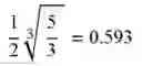
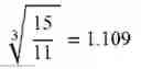
The optimum sizes for different switches at various settings are listed in the following table.
| Rswp1 | Rswp2 | |
| Attenuation (dB) | (multiple of Rswf) | (multiple of Rswf) |
| 0 | OFF | OFF |
| 6 | 1 2 5 3 3 = 0.593 | OFF |
| 12 | 0.5 (arbitrarily chosen) | 15 11 3 = 1.109 |
For this design example, all switches to the (differential) input VGP are of same size, and have same resistance Rswf when ON.
For higher attenuations multiple optimum combinations are possible for Rswp1/2 values. Rswp1 can be arbitrarily fixed to obtain optimum Rswp2.
FIGS. 5A and 5B functionally illustrate respectively a 2-step and 3-step programmable resistor attenuator 10 and 20 (half differential). FIGS. 5A and 5B are used in describing the following illustrative design examples.
For the following 2-step and 3-step-6 dB design examples, values are single-ended, but example implementation is differential.
For the 2-step design example: R=50 ohms, Rswf=3.2 ohms (75 fingers of a unit W/L); Optimum Rswp=1.186*Rswf (63 fingers); If=10 mA at 2 GHz; and for IMD3 f1=2 GHz, f2=2.2 GHz.
For the 3-step design example: Rs=50 ohms, Rswf=4 ohms (60 fingers of a unit W/L); If=10 mA at 2 GHz; and for IMD3 f1=2 GHz, f2=2.2 GHz.
For these design examples, illustrative simulation results for HD3 and IMD3 were as follows.
HD3 in 2-step attenuator: For fingers of Swf=75, optimum fingers for Swp from calculation˜63. HD3 sweep with Swp fingers shows minimum at around 63. An improvement of around 8 dB is seen compared to the case which uses Rswf=Rswp (pmp=75).
IMD3 in 2-step attenuator: With two tones, plots of 2f2-f1 and 2f1-f2 are shown for the 2 step attenuator. Optimum occurs˜60 fingers. An improvement of around 14 dB is seen for IMD tones compared to Rswp=Rswf case.
HD3 in 3-step attenuator at 6 dB: For fingers of Swf=60, optimum fingers for Swp1 at 6 dB from calculation˜101. HD3 sweep with Swp fingers shows minimum at around 100. An improvement of around 6 dB is seen compared to the case which uses Rswp1=Rswf/2 (pmp1=120).
IMD3 in 3-step attenuator at 6 dB: With two tones, plots of 2f2-f1 and 2f1-f2 are shown for 6 dB case. Optimum occurs˜100 fingers. An improvement of around 14 dB is seen for IMD tones compared to Rswp1=Rswf/2 case.
HD3 in 3-step attenuator at 12 dB: For fingers of Swf=60 & of Swp1=120, optimum fingers for Swp2 at 12 dB from calculation˜54. HD3 sweep with Swp fingers shows minimum at around 54. An improvement of around 8 dB is seen compared to the case which uses Rswp2=Rswf (pmp2=60)
IMD3 in 3-step attenuator at 12 dB: With two tones, plots of 2f2-f1 and 2f1-f2 are shown for 12 dB case. Optimum occurs˜54 fingers. An improvement of around 12 dB is seen for IMD tones compared to Rswp2=Rswf case.
HD3 sweeps in 3-step attenuator at 12 dB: Nested sweeps of fingers of Swf and Swp2 for 12 dB case in which Swf fingers are swept from 50 to 70 and Swp2 from 40 to 70. The optimum of Swp2 shifted with Swf variation, and cancellation progressively improved with higher fingers of Swf.
Advantages of the programmable (multistep) resistor attenuator with switch distortion cancellation include. Cancellation of harmonic current of virtual ground switches with that of differential ground switches by optimum switch sizing (Swp and Swf) by exploiting matching between switches (transistors) and ratios of resistors. Due to this distortion cancellation, to meet a given distortion specification, switch sizes can be reduced, with attendant reduced area and parasitics on virtual ground. Distortion cancellation is robust across PVT, input amplitude and frequency, since it relies on ratio of resistors and matching of transistor switches.
The Disclosure provided by this Description and the Figures sets forth example embodiments and applications illustrating aspects and features of the invention, and does not limit the scope of the invention, which is defined by the claims. Known circuits, functions and operations are not described in detail to avoid obscuring the principles and features of the invention. These example embodiments and applications can be used by ordinarily skilled artisans as a basis for modifications, substitutions and alternatives to construct other embodiments, including adaptations for other applications.
Claims
1. A resistor attenuator circuit suitable for programmable attenuation of an input signal, comprising
an input node coupled to receive the input signal;
an virtual ground node configured as a virtual ground;
at least one attenuation stage coupled at an attenuation node to the input node and the virtual ground node, the attenuation node
coupled to the input node through a resistor R,
coupled to the virtual ground node through a resistor kR and a virtual ground switch Swf with an on resistance Rswf, and
coupled to a differential ground through a resistor mR and a differential ground switch Swp with an on resistance Rswp;
Swp is sized relative to Swf such that, when both Swp and Swf are conducting, a component Ipnf of a current Ipn through Rswp and mR to the attenuation node and branching into kR and Rswf, matches, in phase and magnitude, a harmonic current Ifn from the virtual ground through Rswf and kR to the attenuation node, thereby substantially canceling the harmonic distortion appearing at the virtual ground.
2. The circuit of claim 1, wherein Ipnf and Ifn are matched in phase and magnitude based on biasing Swp and Swf.
3. The circuit of claim 1, wherein the virtual ground node is an input to a differential amplifier.
4. The circuit of claim 1, wherein R, mR and kR are matched resistors configured to provide a selected level of attenuation.
5. The circuit of claim 1, further comprising multiple attenuation stages, with associated switches Swp and Swf controlled to provide multiple steps of attenuation.
Images & Drawings included:


Sources:
- United States Patent and Trademark Office - verify current appl. status at the USPTO↗
Recent applications in this class:
- » 20240405741 2024-12-05
Distributed Attenuators With Uniform Electric Field - » 20230246622 2023-08-03
ELECTRONIC CIRCUIT - » 20220407490 2022-12-22
Wideband signal attenuator - » 20200083858 2020-03-12
RF signal aggregator and antenna system implementing the same - » 20190115899 2019-04-18
RF signal aggregator and antenna system implementing the same - » 20180091112 2018-03-29
DEVICE FOR ATTENUATING ELECTROMAGNETIC WAVE AND REDUCING SIDE EFFECTS USING LONGITIDINAL WAVE - » 20160268991 2016-09-15
Radio frequency (RF) series attenuator module for bridging two RF transmission lines on adjacent circuit substrates - » 20160164486 2016-06-09
Transformer filter arrangement - » 20150381139 2015-12-31
Calibration of step attenuator - » 20150365063 2015-12-17
LUMPED ELEMENT FREQUENCY SELECTIVE LIMITERS
Recent applications for this Assignee:
- » 20250291595 2025-09-18
CIRCUIT, SYSTEM, AND METHOD FOR MATRIX DECIMATION - » 20250286550 2025-09-11
TRANSISTOR SHUTDOWN CIRCUT - » 20250279725 2025-09-04
CONDUCTION MODE CONTROL - » 20250274138 2025-08-28
SWITCH REGULATOR - » 20250267687 2025-08-21
ENHANCED BROADCAST TRANSMISSION IN UNSLOTTED CHANNEL HOPPING MEDIUM ACCESS CONTROL - » 20250266825 2025-08-21
BOOTSTRAP CIRCUIT - » 20250247097 2025-07-31
LEVEL SHIFTER CIRCUIT - » 20250247082 2025-07-31
LOW AREA AND POWER MULTI-BIT FLIP-FLOP - » 20250246995 2025-07-31
SWITCHING CONVERTER DEADTIME CONTROL - » 20250246345 2025-07-31
TRIMMING RESISTOR USING MODULATED SIGNAL