Molding compound supported RDL for IC package
US20160118312A1
2016-04-28
14/522,760
2014-10-24
✅ Patent granted
US 9,502,322 B2
2016-11-22
-
-
Errol Fernandes | Brian Turner
Hauptman Ham, LLP
2034-10-24
Abstract:
One of the embodiments for a package substrate discloses a molding compound having plurality of metal pillar with middle portion embedded therein; a top end of the metal pillar protrudes above the molding compound; a bottom end of the metal pillar protrudes below the molding compound; a bottom RDL is configured on bottom of the molding compound; the RDL has a plurality of top metal pad and a plurality of bottom metal pad; a density of the plurality of bottom metal pad is higher than the density of the plurality of top metal pad; each metal pillar metal pad is electrically coupled to a corresponding first top metal pad.
Applicant:
Interested in similar patents?
Get notified when new applications in this technology area are published.
Classification:
H01L21/48 IPC
Processes or apparatus adapted for the manufacture or treatment of semiconductor or solid state devices or of parts thereof; Manufacture or treatment of semiconductor devices or of parts thereof the devices having at least one potential-jump barrier or surface barrier, e.g. PN junction, depletion layer or carrier concentration layer Manufacture or treatment of parts, e.g. containers, prior to assembly of the devices, using processes not provided for in a single one of the subgroups -
H05K1/02 IPC
Printed circuits Details
H05K1/02 IPC
Printed circuits Details
H05K1/0298 » CPC further
Printed circuits; Details; Conductive pattern lay-out details not covered by sub groups - Multilayer circuits
H05K1/0298 » CPC further
Printed circuits; Details; Conductive pattern lay-out details not covered by sub groups - Multilayer circuits
H05K1/111 » CPC further
Printed circuits; Details; Printed elements for providing electric connections to or between printed circuits Pads for surface mounting, e.g. lay-out
H05K1/111 » CPC further
Printed circuits; Details; Printed elements for providing electric connections to or between printed circuits Pads for surface mounting, e.g. lay-out
H05K1/11 IPC
Printed circuits; Details Printed elements for providing electric connections to or between printed circuits
H05K1/11 IPC
Printed circuits; Details Printed elements for providing electric connections to or between printed circuits
H01L23/14 » CPC main
Details of semiconductor or other solid state devices; Mountings, e.g. non-detachable insulating substrates characterised by the material or its electrical properties
H01L21/481 » CPC further
Processes or apparatus adapted for the manufacture or treatment of semiconductor or solid state devices or of parts thereof; Manufacture or treatment of semiconductor devices or of parts thereof the devices having at least one potential-jump barrier or surface barrier, e.g. PN junction, depletion layer or carrier concentration layer; Manufacture or treatment of parts, e.g. containers, prior to assembly of the devices, using processes not provided for in a single one of the subgroups -; Insulating or insulated parts, e.g. mountings, containers, diamond heatsinks Insulating layers on insulating parts, with or without metallisation
H05K3/46 IPC
Apparatus or processes for manufacturing printed circuits Manufacturing multilayer circuits
H05K3/46 IPC
Apparatus or processes for manufacturing printed circuits Manufacturing multilayer circuits
H05K3/28 » CPC further
Apparatus or processes for manufacturing printed circuits; Secondary treatment of printed circuits Applying non-metallic protective coatings
H05K3/28 » CPC further
Apparatus or processes for manufacturing printed circuits; Secondary treatment of printed circuits Applying non-metallic protective coatings
H05K3/4644 » CPC further
Apparatus or processes for manufacturing printed circuits; Manufacturing multilayer circuits by building the multilayer layer by layer, i.e. build-up multilayer circuits
H05K3/4644 » CPC further
Apparatus or processes for manufacturing printed circuits; Manufacturing multilayer circuits by building the multilayer layer by layer, i.e. build-up multilayer circuits
H01L24/97 » CPC further
Arrangements for connecting or disconnecting semiconductor or solid-state bodies; Methods or apparatus related thereto; Batch processes at chip-level, i.e. with connecting carried out on a plurality of singulated devices, i.e. on diced chips the devices being connected to a common substrate, e.g. interposer, said common substrate being separable into individual assemblies after connecting
H01L2224/73204 » CPC further
Indexing scheme for arrangements for connecting or disconnecting semiconductor or solid-state bodies and methods related thereto as covered by; Means for bonding being of different types provided for in two or more of groups; Location after the connecting process on the same surface; Bump and layer connectors the bump connector being embedded into the layer connector
H01L2924/15174 » CPC further
Indexing scheme for arrangements or methods for connecting or disconnecting semiconductor or solid-state bodies as covered by; Details of package parts other than the semiconductor or other solid state devices to be connected; Die mounting substrate; Multilayer substrate; Fan-out arrangement of the internal vias in different layers of the multilayer substrate
H01L2924/15311 » CPC further
Indexing scheme for arrangements or methods for connecting or disconnecting semiconductor or solid-state bodies as covered by; Details of package parts other than the semiconductor or other solid state devices to be connected; Die mounting substrate; Connection portion the connection portion being formed only on the surface of the substrate opposite to the die mounting surface being a ball array, e.g. BGA
H05K2203/14 » CPC further
Indexing scheme relating to apparatus or processes for manufacturing printed circuits covered by Related to the order of processing steps
H05K2203/14 » CPC further
Indexing scheme relating to apparatus or processes for manufacturing printed circuits covered by Related to the order of processing steps
H01L23/00 IPC
Details of semiconductor or other solid state devices
H01L23/13 IPC
Details of semiconductor or other solid state devices; Mountings, e.g. non-detachable insulating substrates characterised by the shape
H01L23/48 IPC
Details of semiconductor or other solid state devices Arrangements for conducting electric current to or from the solid state body in operation, e.g. leads, terminal arrangements ; Selection of materials therefor
H05K3/40 IPC
Apparatus or processes for manufacturing printed circuits Forming printed elements for providing electric connections to or between printed circuits
H05K3/40 IPC
Apparatus or processes for manufacturing printed circuits Forming printed elements for providing electric connections to or between printed circuits
H05K2203/07 » CPC further
Indexing scheme relating to apparatus or processes for manufacturing printed circuits covered by Treatments involving liquids, e.g. plating, rinsing
H05K2203/07 » CPC further
Indexing scheme relating to apparatus or processes for manufacturing printed circuits covered by Treatments involving liquids, e.g. plating, rinsing
Description
BACKGROUND
1. Technical Field
The present invention relates to a redistribution layer (RDL) for IC package, especially relates to an RDL supported by molding compound.
2. Description of Related Art
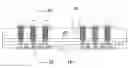
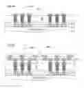
FIG. 1A shows a prior art substrate for IC package
FIG. 1A shows a prior art substrate for IC package disclosed in US2014/0102777A1 which has an embedded silicon interposer 20. The silicon interposer 20 has four lateral sides 206. A molding compound 22 wraps the silicon interposer 20 around the four lateral sides 206. A plurality of via metal 200 is made through the silicon interposer 20. An insulation liner 201 is made between the through via 200 and the silicon interposer 20 for an electrical insulation there-between. A top redistribution layer 21 is made on top of the silicon interposer 20 with a plurality of metal pad 210 exposed on top. The plurality of metal pad 210 on top is provided for accommodating an IC chip (not shown) to mount. A circuit built-up layer 25 is made on bottom of the silicon interposer 20 with a plurality of metal pad 220 configured on bottom. A plurality of solder ball 24 is configured and each solder ball 24 is configured on bottom of a corresponding bottom metal pad 220.
FIG. 1B shows a reversed view of FIG. 1A. FIG. 1B is made to present the prior art of FIG. 1A in a position similar to a package substrate of the present invention to facilitate a comparison there between. FIG. 1B shows an up-down view of FIG. 1A. The top solder ball 24 is configured for mounting the package substrate onto a mother board (not shown). The bottom metal pad 210 is configured for a chip or chips to mount.
BRIEF DESCRIPTION OF THE DRAWINGS
FIG. 1A˜1B show a prior art substrate for IC package
FIGS. 2A˜2L and 3A˜3C, shows a manufacturing process according to the present invention.
FIG. 3D is a first embodiment of the present invention.
FIG. 3E is a second embodiment of the present invention.
FIG. 3F shows an IC chip mounted on bottom of FIG. 3D
FIG. 3F′ shows an IC chip mounted on bottom of FIG. 3E
FIG. 3G shows an IC package unit obtained through singulating the product of FIG. 3F.
FIG. 3G′ shows an IC package unit obtained through singulating the product of FIG. 3F′
FIGS. 2A˜2L and 4A˜4C, shows a manufacturing process according to the present invention.
FIG. 4D is a third embodiment of the present invention.
FIG. 4E is a fourth embodiment of the present invention.
FIG. 4F shows an IC chip mounted on bottom of FIG. 4D
FIG. 4F′ shows an IC chip mounted on bottom of FIG. 4E
FIG. 4G shows an IC package unit obtained through singulating the product of FIG. 4F.
FIG. 4G′ shows an IC package unit obtained through singulating the product of FIG. 4F′
FIGS. 2A˜2L and 5A˜5C, shows a manufacturing process according to the present invention.
FIG. 5D is a fifth embodiment of the present invention.
FIG. 5E is a sixth embodiment of the present invention.
FIG. 5F shows an IC chip mounted on bottom of FIG. 5D
FIG. 5F′ shows an IC chip mounted on bottom of FIG. 5E
FIG. 5G shows an IC package unit obtained through singulating the product of FIG. 5F.
FIG. 5G′ shows an IC package unit obtained through singulating the product of FIG. 5F′
DETAILED DESCRIPTION OF THE INVENTION
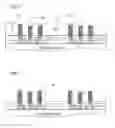
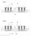
FIGS. 2A˜2L and 3A˜3C, shows a manufacturing process according to the present invention.
FIG. 3D is a first embodiment of the present invention.
FIG. 3E is a second embodiment of the present invention.
A molding compound supported RDL for IC package is fabricated, includes the following steps:
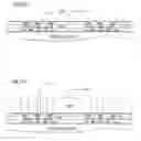
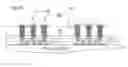
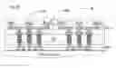
FIG. 2A shows: preparing a temporary carrier; applying a release layer 31 on top of the temporary carrier; and applying a bottom seed layer 32 on top of the release layer 31.
FIG. 2B shows: applying a patterned photo resist 33 on top of the bottom seed layer 32.
FIG. 2C shows: forming a patterned first bottom metal pad 341.
FIG. 2D shows: stripping the photo-resist 33.
FIG. 2E shows: stripping the bottom seed layer 32 between the first bottom metal pads 341.
FIG. 2F shows: forming a bottom RDL (RDL 1) using the first bottom metal pad 341 as a starting point; forming a plurality of first top metal pad 343 on top of the bottom RDL (RDL 1), wherein at least one circuit layer 342 is made between the first bottom metal pad 341 and the first top metal pad 343. A first top dielectric layer 353 is formed on top of the first top metal pad 343 and a plurality opening is made to expose a top of each first top metal pad 343. The first bottom metal pad 341, circuit layer 342, and the first top metal pad 343 are embedded in the dielectric layers 351, 352, 353; forming a first top dielectric layer with a plurality of opening, each opening exposes a top of a corresponding first top metal pad;
FIG. 2G shows: applying a seed layer 352 on top of the first top dielectric layer 353 and the first top metal pad;
FIG. 2H shows: forming a patterned photo resist 332 on top of the seed layer 352;
FIG. 2I shows: forming a plurality of metal pillar 36, each is formed on top of a corresponding first top metal pad 343;
FIG. 2J show: stripping the photo resist 332 and leaving the metal pillar 36 exposed;
stripping the top seed layer 322 between metal pillars 36;
revealing the plurality of metal pillar;
FIG. 2K shows: applying a molding compound 37 to encapsulate the plurality of metal pillar 36;
FIG. 2L shows: thinning from top of the molding compound 37; and
revealing a top surface of each metal pillar 36.
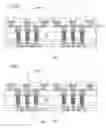
FIG. 3A shows: removing portion of the molding compound 37 from top;
revealing a top end of each metal pillar 36;
FIG. 3B shows: forming a protection layer 361, such as an Electroless Nickel/Electroless Palladium/Immersion Gold (ENEPIG), on each revealed top of the metal pillar 36;
FIG. 3C shows: planting a plurality of solder ball 38, each is planted on top of a corresponding ENEPIG 361 which brackets a top end of a corresponding metal pillar 36;
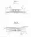
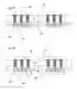
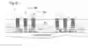
FIG. 3D shows: removing the temporary carrier; and removing the bottom seed layer 32 from bottom of each first bottom metal pad 341. FIG. 3D shows a molding compound 37 wrapping a plurality of metal pillar 36, a protection layer 361 is configured on top of a corresponding metal pillar 36; a solder ball is configured on top of each protection layer 361; a bottom RDL (RDL 1) is made on bottom of the molding compound 37.
FIG. 3E shows: forming a bottom protection layer 39 on bottom of a corresponding first bottom metal pad 341. The protection layer is ENEPIG. The protection layer prevents oxidation of the exposed end of the metal pillar 36 before next step. FIG. 3E shows a molding compound 37 wrapping a plurality of metal pillar 36, a protection layer 361 is configured on top of a corresponding metal pillar 36; a solder ball is configured on top of each protection layer 361; a bottom RDL (RDL 1) is made on bottom of the molding compound 37; a bottom protection layer 39 is made on bottom of a corresponding first bottom metal pad 341.
FIG. 3F shows an IC chip mounted on bottom of FIG. 3D
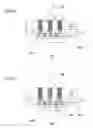
FIG. 3F shows a chip 391 mounted on bottom of FIG. 3D; the chip 391 is electrically coupled to the first bottom metal pad 341 through a plurality of solder ball. An under fill 392 can be made between the chip 391 and the first bottom metal pad 341.
FIG. 3F′ shows an IC chip mounted on bottom of FIG. 3E
FIG. 3F′ shows a chip 391 mounted on bottom of FIG. 3E; the chip 391 is electrically coupled to the bottom protection layer 39 through a plurality of solder ball. An under fill 392 can be made between the chip 391 and the bottom protection layer 39.
FIG. 3G shows an IC package unit obtained through singulating the product of FIG. 3F.
FIG. 3G shows an IC package which is a package based on the molding compound supported RDL of the first embodiment according to the present invention.
FIG. 3G′ shows an IC package unit obtained through singulating the product of FIG. 3F′
FIG. 3G′ shows an IC package which is a package based on the molding compound supported RDL of the second embodiment according to the present invention.
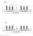
FIGS. 2A˜2L and 4A˜4C, shows a manufacturing process according to the present invention.
FIG. 4D is a third embodiment of the present invention.
FIG. 4E is a fourth embodiment of the present invention.
The manufacturing process of FIGS. 2A˜2L is the same as described in previous paragraph and omitted here for simplification.
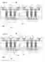
FIG. 4A shows: removing portion of the molding compound 37 from top;
revealing a top end of each metal pillar 36;
FIG. 4B shows: forming a protection layer 362, such as an Organic Solderability Preservatives (OSP), on each revealed top of the metal pillar 36. The protection layer prevents oxidation of the exposed end of the metal pillar 36 before next step.
FIG. 4C shows: planting a plurality of solder ball 38, each is planted on top of a corresponding protection layer 362, however OSP is cleaned out by soldering flux and heat; therefore, the solder ball 38 can be seen planted directly on a top of a corresponding metal pillar 36.
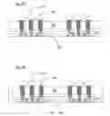
FIG. 4D shows: removing the temporary carrier; and removing the seed layer 32 from bottom of each first bottom metal pad 341.
FIG. 4E shows: forming a bottom protection layer 39 on bottom of a corresponding first bottom metal pad 341. The protection layer is ENEPIG. FIG. 4E shows a molding compound 37 wrapping a plurality of metal pillar 36; a solder ball is configured on top of a corresponding metal pillar 36; a bottom RDL (RDL 1) is made on bottom of the molding compound 37; a bottom protection layer 39 is made on bottom of a corresponding first bottom metal pad 341.
FIG. 4F shows an IC chip mounted on bottom of FIG. 4D
FIG. 4F shows an IC chip mounted on bottom of FIG. 4D; the chip 391 is electrically coupled to the first bottom metal pad 341 through a plurality of solder ball. An under fill 392 can be made between the chip 391 and the first bottom metal pad 341.
FIG. 4F′ shows an IC chip mounted on bottom of FIG. 4E
FIG. 4F′ shows an IC chip 391 mounted on bottom of FIG. 4E; the chip 391 is electrically coupled to the bottom protection layer 39 through a plurality of solder ball. An under fill 392 can be made between the chip 391 and the bottom protection layer 39.
FIG. 4G shows an IC package unit obtained through singulating the product of FIG. 4F.
FIG. 4G shows an IC package which is a package based on the molding compound supported RDL of the third embodiment according to the present invention.
FIG. 4G′ shows an IC package unit obtained through singulating the product of FIG. 4F′
FIG. 4G′ shows an IC package which is a package based on the molding compound supported RDL of the fourth embodiment according to the present invention.
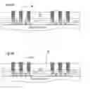
FIGS. 2A˜2L and 5A˜5C, shows a manufacturing process according to the present invention.
FIG. 5D is a fifth embodiment of the present invention.
FIG. 5E is a sixth embodiment of the present invention.
The manufacturing process of FIGS. 2A˜2L is the same as described in previous paragraph and omitted here for simplification.
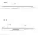
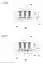
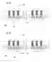
FIG. 5A shows: forming a second bottom metal pad 441 on top of a corresponding metal pillar 36;
FIG. 5B shows: forming a top RDL (RDL 2) on top of the molding compound 37; forming a plurality of second top metal pad 443 on top of the top RDL (RDL 2);
FIG. 5C shows: planting a plurality of solder ball 38, each is planted on top of a corresponding second top metal pad;
FIG. 5D shows: removing the temporary carrier; and removing the bottom seed layer 32 from bottom of each first bottom metal pad 341.
FIG. 5E shows: forming a bottom protection layer 39 on bottom of a corresponding first bottom metal pad 341.
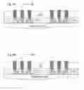
FIG. 5F shows an IC chip mounted on bottom of FIG. 5D
FIG. 5F shows an IC chip mounted on bottom of FIG. 5D; the chip 391 is electrically coupled to the first bottom metal pad 341 through a plurality of solder ball. An under fill 392 can be made between the chip 391 and the first bottom metal pad 341.
FIG. 5F′ shows an IC chip mounted on bottom of FIG. 5E
FIG. 5F′ shows an IC chip 391 mounted on bottom of FIG. 5E; the chip 391 is electrically coupled to the bottom protection layer 39 through a plurality of solder ball. An under fill 392 can be made between the chip 391 and the bottom protection layer 39.
FIG. 5G shows an IC package unit obtained through singulating the product of FIG. 5F.
FIG. 5G shows an IC package which is a package based on the molding compound supported RDL of the fifth embodiment according to the present invention.
FIG. 5G′ shows an IC package unit obtained through singulating the product of FIG. 5F′
FIG. 5G′ shows an IC package which is a package based on the molding compound supported RDL of the sixth embodiment according to the present invention.
While several embodiments have been described by way of example, it will be apparent to those skilled in the art that various modifications may be configured without departs from the spirit of the present invention. Such modifications are all within the scope of the present invention, as defined by the appended claims.
Claims
1. A molding compound supported redistribution layer (RDL) structure for an integrated circuit (IC) package, the RDL structure comprising:
a molding compound;
a plurality of metal pillars, each extending through the molding compound and having
a bottom end protruded below the molding compound;
a bottom RDL configured on bottom of the molding compound and having
a plurality of first bottom metal pads, and
a plurality of first top metal pads; and
a chip mounted on the plurality of first bottom metal pads,
wherein
a density of the plurality of first bottom metal pads is higher than a density of the plurality of first top metal pads,
the bottom end of each metal pillar among the plurality of metal pillars is electrically coupled to a corresponding first top metal pad among the plurality of first top metal pads, and
in a thickness direction of the RDL structure, the bottom RDL is arranged between the chip and the plurality of metal pillars.
2. A molding compound supported RDL structure as claimed in claim 1, further comprising:
a top protection layer bracketing a top end of a corresponding metal pillar among the plurality of metal pillars, the top end protruded above the molding compound.
3. A molding compound supported RDL structure as claimed in claim 2, wherein the top protection layer is selected from the group consisting of Electroless Nickel/Electroless Palladium/Immersion Gold (ENEPIG) and Organic Solderability Preservatives (OSP).
4. A molding compound supported RDL structure as claimed in claim 2, further comprising:
a plurality of solder balls, each configured on top of the top protection layer bracketing the top end of a corresponding metal pillar among the plurality of metal pillars.
5. A molding compound supported RDL structure as claimed in claim 1, further comprising:
a plurality of solder balls, each directly configured on top of a corresponding metal pillar among the plurality of metal pillars.
6. A molding compound supported RDL structure as claimed in claim 4, further comprising:
a bottom protection layer configured on bottom of a corresponding first bottom metal pad among the plurality of first bottom metal pads.
7. A molding compound supported RDL structure as claimed in claim 6, wherein the bottom protection layer is selected from the group consisting of ENEPIG and OSP.
8. A molding compound supported RDL structure as claimed in claim 5, further comprising:
a bottom protection layer configured on bottom of a corresponding first bottom metal pad among the plurality of first bottom metal pads.
9. A molding compound supported RDL structure as claimed in claim 8, wherein the bottom protection layer is selected from the group consisting of ENEPIG and OSP.
10. A molding compound supported redistribution layer (RDL) structure for an integrated circuit (IC) package, the RDL structure comprising:
a molding compound;
a plurality of metal pillars, each extending through the molding compound and having
a top surface coplanar with a top surface of the molding compound, and
bottom end protruded below the molding compound; and
a bottom RDL configured on bottom of the molding compound and having
a plurality of first bottom metal pads, and
a plurality of first top metal pads,
wherein
a density of the plurality of first bottom metal pads is higher than a density of the plurality of first top metal pads,
the bottom end of each metal pillar among the plurality of metal pillars is electrically coupled to a corresponding first top metal pad among the plurality of first top metal pads,
the bottom RDL further comprises a topmost dielectric layer, and
the plurality of first top metal pads and the bottom end of each metal pillar among the plurality of metal pillars are embedded in the topmost dielectric layer.
11. A molding compound supported RDL structure as claimed in claim 10, further comprising:
a top RDL configured on top of the molding compound and having
a plurality of second bottom metal pads on top of the plurality of metal pillars, and
a plurality of second top metal pads,
wherein
a density of the plurality of second bottom metal pads is higher than a density of the plurality of second top metal pads; and
the top surface of each metal pillar among the plurality of metal pillars is electrically coupled to a corresponding second bottom metal pad among the plurality of second bottom metal pads.
12. A molding compound supported RDL structure as claimed in claim 11, further comprising:
a plurality of solder balls, each configured on top of a corresponding second top metal pad among the plurality of second top metal pads.
13. A molding compound supported RDL structure as claimed in claim 10, further comprising:
a bottom protection layer configured on bottom of a corresponding first bottom metal pad among the plurality of first bottom metal pads.
14. A molding compound supported RDL structure as claimed in claim 13, wherein the bottom protection layer is selected from the group consisting of ENEPIG and OSP.
15. A fabricating process for a molding compound supported redistribution layer (RDL) structure for an integrated circuit (IC) package, the fabricating process comprising:
applying a release layer on top of a temporary carrier;
applying a bottom seed layer on top of the releasing layer;
applying a first patterned photo resist on top of the bottom seed layer;
forming a plurality of patterned first bottom metal pads;
stripping the first patterned photo resist;
stripping the bottom seed layer between the plurality of first bottom metal pads;
forming a bottom RDL using the plurality of first bottom metal pads as a starting point, the bottom RDL having a plurality of first top metal pads;
forming a first top dielectric layer with a plurality of openings, each exposing a top of a corresponding first top metal pad among the plurality of first top metal pads;
applying a top seed layer on top of the first top dielectric layer and the plurality of first top metal pads;
forming a second patterned photo resist on top of the top seed layer;
forming, in the second patterned photo resist, a plurality of metal pillars, each on top of a corresponding first top metal pad among the plurality of first top metal pads;
stripping the second patterned photo resist;
stripping the top seed layer between the plurality of metal pillars;
applying a molding compound to encapsulate the plurality of metal pillars, wherein each metal pillar among the plurality of metal pillars extends through the molding compound and has a bottom end protruded below the molding compound;
thinning the molding compound from top to expose top ends of the plurality of metal pillars; and
mounting a chip on the plurality of first bottom metal pads,
wherein
a density of the plurality of first bottom metal pads is higher than a density of the plurality of first top metal pads,
the bottom end of each metal pillar among the plurality of metal pillars is electrically coupled to a corresponding first top metal pad among the plurality of first top metal pads, and
in a thickness direction of the RDL structure, the bottom RDL is arranged between the chip and the plurality of metal pillars.
16. A fabricating process for a molding compound supported RDL structure as claimed in claim 15, further comprising:
forming a protection layer bracketing the exposed top end of each metal pillar among the plurality of metal pillars;
planting a plurality of solder balls, each on top of the corresponding top protection layer which brackets the top end of a corresponding metal pillar among the plurality of metal pillars;
removing the temporary carrier; and
removing the bottom seed layer from bottom of each first bottom metal pad among the plurality of first bottom metal pads.
17. A fabricating process for a molding compound supported RDL structure as claimed in claim 16, further comprising:
forming a bottom protection layer on bottom of a corresponding first bottom metal pad among the plurality of first bottom metal pads.
18. A fabricating process for a molding compound supported RDL structure as claimed in claim 15, further comprising:
forming a protection layer bracketing the exposed top end of each metal pillar among the plurality of metal pillars;
planting a plurality of solder balls, each on top of the corresponding top protection layer which brackets the top end of a corresponding metal pillar among the plurality of metal pillars, wherein the top protection layer is cleaned out by soldering flux and heat and each of the plurality of solder balls is directly configured on top of a corresponding metal pillar among the plurality of metal pillars;
removing the temporary carrier; and
removing the bottom seed layer from bottom of each first bottom metal pad among the plurality of first bottom metal pads.
19. A fabricating process for a molding compound supported RDL structure as claimed in claim 18, further comprising:
forming a bottom protection layer on bottom of a corresponding first bottom metal pad among the plurality of first bottom metal pads.
20. A fabricating process for a molding compound supported RDL structure as claimed in claim 15, wherein top surfaces of the exposed top ends of the plurality of metal pillars are coplanar with a top surface of the molding compound, the fabricating process further comprising:
forming a top RDL on top of the molding compound, the top RDL having
a plurality of second bottom metal pads on the top surfaces of the exposed top ends of the plurality of metal pillars; and
a plurality of second top metal pads;
planting a plurality of solder balls, each on top of a corresponding second top metal pad among the plurality of second top metal pads;
removing the temporary carrier; and
removing the bottom seed layer from bottom of each first bottom metal pad among the plurality of first bottom metal pads.
21. A fabricating process for a molding compound supported RDL structure as claimed in claim 20, further comprising:
forming a bottom protection layer on bottom of a corresponding first bottom metal pad among the plurality of first bottom metal pads.
22-23. (canceled)
24. A molding compound supported RDL structure as claimed in claim 1, wherein an entirety of the chip is below the bottom RDL and the molding compound.
25. A molding compound supported RDL structure as claimed in claim 10, further comprising:
a chip mounted on the plurality of first bottom metal pads,
wherein an entirety of the chip is below the bottom RDL and the molding compound.
Images & Drawings included:


Sources:
- United States Patent and Trademark Office - verify current appl. status at the USPTO↗
Similar patent applications:
- » 20160118328
Molding compound supported RDL for IC package
Recent applications in this class:
- » 20250174504 2025-05-29
METHOD FOR MANUFACTURING SEMICONDUCTOR DEVICE, SEMICONDUCTOR DEVICE, AND SEMICONDUCTOR MEMBER - » 20240421010 2024-12-19
SINTER BONDING SHEET ROLL - » 20240282651 2024-08-22
ELECTRONIC ELEMENT MOUNTING SUBSTRATE - » 20240170354 2024-05-23
SEMICONDUCTOR DEVICE AND METHOD OF MANUFACTURING SEMICONDUCTOR DEVICE - » 20240047285 2024-02-08
SEMICONDUCTOR DEVICES WITH FLEXIBLE SPACER - » 20220037220 2022-02-03
Wiring substrate, electronic device, and electronic module - » 20210366799 2021-11-25
Semiconductor package and method of manufacturing the same - » 20210327776 2021-10-21
Circuit structure and electrical junction box - » 20210280480 2021-09-09
Semiconductor device having a resin layer sealing a plurality of semiconductor chips stacked on first semiconductor chips - » 20210159133 2021-05-27
Circuit module and communication device