Molding compound supported RDL for IC package
US20160118328A1
2016-04-28
14/559,696
2014-12-03
✅ Patent granted
US 9,431,335 B2
2016-08-30
-
-
Kimberly Rizkallah | Brian Turner
Hauptman Ham, LLP
2034-12-03
Abstract:
A cylindrical molding compound supported RDL for IC package is disclosed wherein a central cavity is formed in the center of the molding compound. A plurality of metal pillar is embedded in the molding compound, a redistribution layer is configured on bottom of the plurality of metal pillar; at least one passive element such as a capacitor can be mounted in the central cavity. The bottom of the package is adaptive for at least one chip to mount so that the passive element is close to the chip and therefore simultaneous switching noise (SSN) can be reduced to a minimum at the initial first stage when a power is turned on.
Applicant:
Interested in similar patents?
Get notified when new applications in this technology area are published.
Classification:
H01L21/486 » CPC further
Processes or apparatus adapted for the manufacture or treatment of semiconductor or solid state devices or of parts thereof; Manufacture or treatment of semiconductor devices or of parts thereof the devices having at least one potential-jump barrier or surface barrier, e.g. PN junction, depletion layer or carrier concentration layer; Manufacture or treatment of parts, e.g. containers, prior to assembly of the devices, using processes not provided for in a single one of the subgroups -; Conductive parts; Leads on or in insulating or insulated substrates, e.g. metallisation Via connections through the substrate with or without pins
H01L21/4853 » CPC further
Processes or apparatus adapted for the manufacture or treatment of semiconductor or solid state devices or of parts thereof; Manufacture or treatment of semiconductor devices or of parts thereof the devices having at least one potential-jump barrier or surface barrier, e.g. PN junction, depletion layer or carrier concentration layer; Manufacture or treatment of parts, e.g. containers, prior to assembly of the devices, using processes not provided for in a single one of the subgroups -; Conductive parts; Leads on or in insulating or insulated substrates, e.g. metallisation Connection or disconnection of other leads to or from a metallisation, e.g. pins, wires, bumps
H01L21/568 » CPC further
Processes or apparatus adapted for the manufacture or treatment of semiconductor or solid state devices or of parts thereof; Manufacture or treatment of semiconductor devices or of parts thereof the devices having at least one potential-jump barrier or surface barrier, e.g. PN junction, depletion layer or carrier concentration layer; Assembly of semiconductor devices using processes or apparatus not provided for in a single one of the subgroups - , e.g. sealing of a cap to a base of a container; Encapsulations, e.g. encapsulation layers, coatings Temporary substrate used as encapsulation process aid
H01L23/49827 » CPC further
Details of semiconductor or other solid state devices; Arrangements for conducting electric current to or from the solid state body in operation, e.g. leads, terminal arrangements ; Selection of materials therefor consisting of soldered constructions; Leads, on insulating substrates, Via connections through the substrates, e.g. pins going through the substrate, coaxial cables
H01L23/49838 » CPC further
Details of semiconductor or other solid state devices; Arrangements for conducting electric current to or from the solid state body in operation, e.g. leads, terminal arrangements ; Selection of materials therefor consisting of soldered constructions; Leads, on insulating substrates, Geometry or layout
H01L23/49861 » CPC further
Details of semiconductor or other solid state devices; Arrangements for conducting electric current to or from the solid state body in operation, e.g. leads, terminal arrangements ; Selection of materials therefor consisting of soldered constructions; Leads, on insulating substrates, Lead-frames fixed on or encapsulated in insulating substrates
H01L23/498 IPC
Details of semiconductor or other solid state devices; Arrangements for conducting electric current to or from the solid state body in operation, e.g. leads, terminal arrangements ; Selection of materials therefor consisting of soldered constructions Leads, on insulating substrates,
H01L21/48 IPC
Processes or apparatus adapted for the manufacture or treatment of semiconductor or solid state devices or of parts thereof; Manufacture or treatment of semiconductor devices or of parts thereof the devices having at least one potential-jump barrier or surface barrier, e.g. PN junction, depletion layer or carrier concentration layer Manufacture or treatment of parts, e.g. containers, prior to assembly of the devices, using processes not provided for in a single one of the subgroups -
H01L21/56 IPC
Processes or apparatus adapted for the manufacture or treatment of semiconductor or solid state devices or of parts thereof; Manufacture or treatment of semiconductor devices or of parts thereof the devices having at least one potential-jump barrier or surface barrier, e.g. PN junction, depletion layer or carrier concentration layer; Assembly of semiconductor devices using processes or apparatus not provided for in a single one of the subgroups - , e.g. sealing of a cap to a base of a container Encapsulations, e.g. encapsulation layers, coatings
H01L23/49894 » CPC main
Details of semiconductor or other solid state devices; Arrangements for conducting electric current to or from the solid state body in operation, e.g. leads, terminal arrangements ; Selection of materials therefor consisting of soldered constructions; Leads, on insulating substrates, characterised by the materials Materials of the insulating layers or coatings
H01L23/49816 » CPC further
Details of semiconductor or other solid state devices; Arrangements for conducting electric current to or from the solid state body in operation, e.g. leads, terminal arrangements ; Selection of materials therefor consisting of soldered constructions; Leads, on insulating substrates,; Additional leads joined to the metallisation on the insulating substrate, e.g. pins, bumps, wires, flat leads Spherical bumps on the substrate for external connection, e.g. ball grid arrays [BGA]
H01L23/48 IPC
Details of semiconductor or other solid state devices Arrangements for conducting electric current to or from the solid state body in operation, e.g. leads, terminal arrangements ; Selection of materials therefor
H01L21/3105 IPC
Processes or apparatus adapted for the manufacture or treatment of semiconductor or solid state devices or of parts thereof; Manufacture or treatment of semiconductor devices or of parts thereof the devices having at least one potential-jump barrier or surface barrier, e.g. PN junction, depletion layer or carrier concentration layer the devices having semiconductor bodies comprising elements of Group IV of the Periodic System or AB compounds with or without impurities, e.g. doping materials; Treatment of semiconductor bodies using processes or apparatus not provided for in groups - to form insulating layers thereon, e.g. for masking or by using photolithographic techniques ; After treatment of these layers; Selection of materials for these layers After-treatment
H01L23/495 IPC
Details of semiconductor or other solid state devices; Arrangements for conducting electric current to or from the solid state body in operation, e.g. leads, terminal arrangements ; Selection of materials therefor consisting of soldered constructions Lead-frames or other flat leads
H01L33/44 IPC
Semiconductor devices with at least one potential-jump barrier or surface barrier specially adapted for light emission; Processes or apparatus specially adapted for the manufacture or treatment thereof or of parts thereof; Details thereof characterised by the coatings, e.g. passivation layer or anti-reflective coating
H01L21/481 » CPC further
Processes or apparatus adapted for the manufacture or treatment of semiconductor or solid state devices or of parts thereof; Manufacture or treatment of semiconductor devices or of parts thereof the devices having at least one potential-jump barrier or surface barrier, e.g. PN junction, depletion layer or carrier concentration layer; Manufacture or treatment of parts, e.g. containers, prior to assembly of the devices, using processes not provided for in a single one of the subgroups -; Insulating or insulated parts, e.g. mountings, containers, diamond heatsinks Insulating layers on insulating parts, with or without metallisation
H01L21/566 » CPC further
Processes or apparatus adapted for the manufacture or treatment of semiconductor or solid state devices or of parts thereof; Manufacture or treatment of semiconductor devices or of parts thereof the devices having at least one potential-jump barrier or surface barrier, e.g. PN junction, depletion layer or carrier concentration layer; Assembly of semiconductor devices using processes or apparatus not provided for in a single one of the subgroups - , e.g. sealing of a cap to a base of a container; Encapsulations, e.g. encapsulation layers, coatings; Moulds Release layers for moulds, e.g. release layers, layers against residue during moulding
H01L31/147 IPC
Semiconductor devices sensitive to infra-red radiation, light, electromagnetic radiation of shorter wavelength or corpuscular radiation and specially adapted either for the conversion of the energy of such radiation into electrical energy or for the control of electrical energy by such radiation; Processes or apparatus specially adapted for the manufacture or treatment thereof or of parts thereof; Details thereof structurally associated with, e.g. formed in or on a common substrate with, one or more electric light sources, e.g. electroluminescent light sources, and electrically or optically coupled thereto the light source or sources being controlled by the semiconductor device sensitive to radiation, e.g. image converters, image amplifiers or image storage devices the light sources and the devices sensitive to radiation all being semiconductor devices characterised by at least one potential or surface barrier
Description
This application is a continuation-in-part application of U.S. application Ser. No. 14/522,760 filed Oct. 24, 2014, the disclosure of which is incorporated by reference herein in its entirety.
BACKGROUND
1. Technical Field
The present invention relates to a redistribution layer (RDL) for IC package, especially relates to an RDL supported by molding compound.
2. Description of Related Art
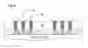
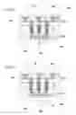
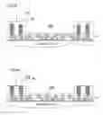
FIG. 1A shows a prior art substrate for IC package
FIG. 1A shows a prior art substrate for IC package disclosed in US2014/0102777A1 which has an embedded silicon interposer 20. The silicon interposer 20 has four lateral sides 206. A molding compound 22 wraps the silicon interposer 20 around the four lateral sides 206. A plurality of via metal 200 is made through the silicon interposer 20. An insulation liner 201 is made between the through via 200 and the silicon interposer 20 for an electrical insulation there-between. A top redistribution layer 21 is made on top of the silicon interposer 20 with a plurality of metal pad 210 exposed on top. The plurality of metal pad 210 on top is provided for accommodating an IC chip (not shown) to mount. A circuit built-up layer 25 is made on bottom of the silicon interposer 20 with a plurality of metal pad 220 configured on bottom. A plurality of solder ball 24 is configured and each solder ball 24 is configured on bottom of a corresponding bottom metal pad 220.
FIG. 1B shows a reversed view of FIG. 1A. FIG. 1B is made to present the prior art of FIG. 1A in a position similar to a package substrate of the present invention to facilitate a comparison there between. FIG. 1B shows an up-down view of FIG. 1A. The top solder ball 24 is configured for mounting the package substrate onto a mother board (not shown). The bottom metal pad 210 is configured for a chip or chips to mount.
BRIEF DESCRIPTION OF THE DRAWINGS
FIG. 1A˜1B show a prior art substrate for IC package
FIGS. 2A˜2L and 3A˜3C, shows a manufacturing process according to the present invention.
FIG. 3D is a first embodiment of the present invention.
FIG. 3E is a second embodiment of the present invention.
FIG. 3F shows an IC chip mounted on bottom of FIG. 3D
FIG. 3F′ shows an IC chip mounted on bottom of FIG. 3E
FIG. 3G shows an IC package unit obtained through singulating the product of FIG. 3F.
FIG. 3G′ shows an IC package unit obtained through singulating the product of FIG. 3F′
FIGS. 2A˜2L and 4A˜4C, shows a manufacturing process according to the present invention.
FIG. 4D is a third embodiment of the present invention.
FIG. 4E is a fourth embodiment of the present invention.
FIG. 4F shows an IC chip mounted on bottom of FIG. 4D
FIG. 4F′ shows an IC chip mounted on bottom of FIG. 4E
FIG. 4G shows an IC package unit obtained through singulating the product of FIG. 4F.
FIG. 4G′ shows an IC package unit obtained through singulating the product of FIG. 4F′
FIGS. 2A˜2L and 5A˜5C, shows a manufacturing process according to the present invention.
FIG. 5D is a fifth embodiment of the present invention.
FIG. 5E is a sixth embodiment of the present invention.
FIG. 5F shows an IC chip mounted on bottom of FIG. 5D
FIG. 5F′ shows an IC chip mounted on bottom of FIG. 5E
FIG. 5G shows an IC package unit obtained through singulating the product of FIG. 5F.
FIG. 5G′ shows an IC package unit obtained through singulating the product of FIG. 5F′
FIG. 6A˜6M is a seventh embodiment of the present invention.
DETAILED DESCRIPTION OF THE INVENTION
FIGS. 2A˜2L and 3A˜3C, Shows a Manufacturing Process According to the Present Invention. FIG. 3D is a First Embodiment of the Present Invention; and FIG. 3E is a Second Embodiment of the Present Invention.
A molding compound supported RDL for IC package is fabricated, includes the following steps:
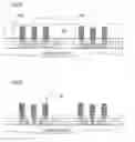
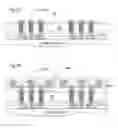
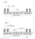
FIG. 2A shows: preparing a temporary carrier; applying a release layer 31 on top of the temporary carrier; and applying a bottom seed layer 32 on top of the release layer 31.
FIG. 2B shows: applying a patterned photo resist 33 on top of the bottom seed layer 32.
FIG. 2C shows: forming a patterned first bottom metal pad 341.
FIG. 2D shows: stripping the photo-resist 33.
FIG. 2E shows: stripping the bottom seed layer 32 between the first bottom metal pads 341.
FIG. 2F shows: forming a bottom RDL (RDL 1) using the first bottom metal pad 341 as a starting point; forming a plurality of first top metal pad 343 on top of the bottom RDL (RDL 1), wherein at least one circuit layer 342 is made between the first bottom metal pad 341 and the first top metal pad 343. A first top dielectric layer 353 is formed on top of the first top metal pad 343 and a plurality opening is made to expose a top of each first top metal pad 343. The first bottom metal pad 341, circuit layer 342, and the first top metal pad 343 are embedded in the dielectric layers 351, 352, 353; forming a first top dielectric layer with a plurality of opening, each opening exposes a top of a corresponding first top metal pad;
FIG. 2G shows: applying a top seed layer 352 on top of the first top dielectric layer 353 and the first top metal pad;
FIG. 2H shows: forming a patterned photo resist 332 on top of the top seed layer 352;
FIG. 2I shows: forming a plurality of metal pillar 36, each is formed on top of a corresponding first top metal pad 343;
FIG. 2J show: stripping the photo resist 332 and leaving the metal pillar 36 exposed;
-
- stripping the top seed layer 322 between metal pillars 36;
- revealing the plurality of metal pillar;
FIG. 2K shows: applying a molding compound 37 to encapsulate the plurality of metal pillar 36;
FIG. 2L shows: thinning from top of the molding compound 37; and
-
- revealing a top surface of each metal pillar 36.
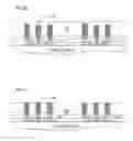
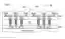
FIG. 3A shows: removing portion of the molding compound 37 from top;
-
- revealing a top end of each metal pillar 36;
FIG. 3B shows: forming a protection layer 361, such as an Electroless Nickel/Electroless Palladium/Immersion Gold (ENEPIG), on each revealed top of the metal pillar 36;
FIG. 3C shows: planting a plurality of solder ball 38, each is planted on top of a corresponding ENEPIG 362 which brackets a top end of a corresponding metal pillar 36;
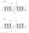
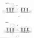
FIG. 3D shows: removing the temporary carrier; and removing the bottom seed layer 32 from bottom of each first bottom metal pad 341. FIG. 3D shows a molding compound 37 wrapping a plurality of metal pillar 36, a protection layer 361 is configured on top of a corresponding metal pillar 36; a solder ball is configured on top of each protection layer 361; a bottom RDL (RDL 1) is made on bottom of the molding compound 37.
FIG. 3E shows: forming a bottom protection layer 39 on bottom of a corresponding first bottom metal pad 341. The protection layer is ENEPIG. The protection layer prevents oxidation of the exposed end of the metal pillar 36 before next step. FIG. 3E shows a molding compound 37 wrapping a plurality of metal pillar 36, a protection layer 361 is configured on top of a corresponding metal pillar 36; a solder ball is configured on top of each protection layer 361; a bottom RDL (RDL 1) is made on bottom of the molding compound 37; a bottom protection layer 39 is made on bottom of a corresponding first bottom metal pad 341.
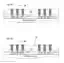
FIG. 3F Shows an IC Chip Mounted on Bottom of FIG. 3D
FIG. 3F shows a chip 391 mounted on bottom of FIG. 3D; the chip 391 is electrically coupled to the first bottom metal pad 341 through a plurality of solder ball. An under fill 392 can be made between the chip 391 and the first bottom metal pad 341.
FIG. 3F′ Shows an IC Chip Mounted on Bottom of FIG. 3E
FIG. 3F′ shows a chip 391 mounted on bottom of FIG. 3E; the chip 391 is electrically coupled to the bottom protection layer 39 through a plurality of solder ball. An under fill 392 can be made between the chip 391 and the bottom protection layer 39.
FIG. 3G Shows an IC Package Unit Obtained through Singulating the Product of FIG. 3F.
FIG. 3G shows an IC package which is a package based on the molding compound supported RDL of the first embodiment according to the present invention.
FIG. 3G′ Shows an IC Package Unit Obtained through Singulating the Product of FIG. 3F′
FIG. 3G′ shows an IC package which is a package based on the molding compound supported RDL of the second embodiment according to the present invention.
FIGS. 2A˜2L and 4A˜4C, Shows a Manufacturing Process According to the Present Invention. FIG. 4D is a Third Embodiment of the Present Invention. FIG. 4E is a Fourth Embodiment of the Present Invention.
The manufacturing process of FIGS. 2A˜2L is the same as described in previous paragraph and omitted here for simplification.
FIG. 4A shows: removing portion of the molding compound 37 from top;
-
- revealing a top end of each metal pillar 36;
FIG. 4B shows: forming a protection layer 362, such as an Organic Solderability Preservatives (OSP), on each revealed top of the metal pillar 36. The protection layer prevents oxidation of the exposed end of the metal pillar 36 before next step.
FIG. 4C shows: planting a plurality of solder ball 38, each is planted on top of a corresponding protection layer 362, however OSP is cleaned out by soldering flux and heat; therefore, the solder ball 38 can be seen planted directly on a top of a corresponding metal pillar 36.
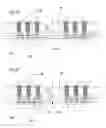
FIG. 4D shows: removing the temporary carrier; and removing the seed layer 32 from bottom of each first bottom metal pad 341.
FIG. 4E shows: forming a bottom protection layer 39 on bottom of a corresponding first bottom metal pad 341. The protection layer is ENEPIG. FIG. 4E shows a molding compound 37 wrapping a plurality of metal pillar 36; a solder ball is configured on top of a corresponding metal pillar 36; a bottom RDL (RDL 1) is made on bottom of the molding compound 37; a bottom protection layer 39 is made on bottom of a corresponding first bottom metal pad 341.
FIG. 4F Shows an IC Chip Mounted on Bottom of FIG. 4D
FIG. 4F shows an IC chip mounted on bottom of FIG. 4D; the chip 391 is electrically coupled to the first bottom metal pad 341 through a plurality of solder ball. An under fill 392 can be made between the chip 391 and the first bottom metal pad 341.
FIG. 4F′ Shows an IC Chip Mounted on Bottom of FIG. 4E
FIG. 4F′ shows an IC chip 391 mounted on bottom of FIG. 4E; the chip 391 is electrically coupled to the bottom protection layer 39 through a plurality of solder ball. An under fill 392 can be made between the chip 391 and the bottom protection layer 39.
FIG. 4G Shows an IC Package Unit Obtained through Singulating the Product of FIG. 4F.
FIG. 4G shows an IC package which is a package based on the molding compound supported RDL of the third embodiment according to the present invention.
FIG. 4G′ Shows an IC Package Unit Obtained through Singulating the Product of FIG. 4F′
FIG. 4G′ shows an IC package which is a package based on the molding compound supported RDL of the fourth embodiment according to the present invention.
FIGS. 2A˜2L and 5A˜5C, Shows a Manufacturing Process According to the Present Invention. FIG. 5D is a Fifth Embodiment of the Present Invention. FIG. 5E is a Sixth Embodiment of the Present Invention.
The manufacturing process of FIGS. 2A˜2L is the same as described in previous paragraph and omitted here for simplification.
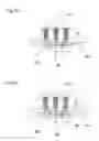
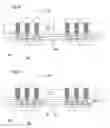
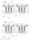
FIG. 5A shows: forming a second bottom metal pad 441 on top of a corresponding metal pillar 36;
FIG. 5B shows: forming a top RDL (RDL 2) on top of the molding compound 37; forming a plurality of second top metal pad 443 on top of the top RDL (RDL 2);
FIG. 5C shows: planting a plurality of solder ball 38, each is planted on top of a corresponding second top metal pad;
FIG. 5D shows: removing the temporary carrier; and removing the bottom seed layer 32 from bottom of each first bottom metal pad 341.
FIG. 5E shows: forming a bottom protection layer 39 on bottom of a corresponding first bottom metal pad 341.
FIG. 5F Shows an IC Chip Mounted on Bottom of FIG. 5D
FIG. 5F shows an IC chip mounted on bottom of FIG. 5D; the chip 391 is electrically coupled to the first bottom metal pad 341 through a plurality of solder ball. An under fill 392 can be made between the chip 391 and the first bottom metal pad 341.
FIG. 5F′ Shows an IC Chip Mounted on Bottom of FIG. 5E
FIG. 5F′ shows an IC chip 391 mounted on bottom of FIG. 5E; the chip 391 is electrically coupled to the bottom protection layer 39 through a plurality of solder ball. An under fill 392 can be made between the chip 391 and the bottom protection layer 39.
FIG. 5G Shows an IC Package Unit Obtained through Singulating the Product of FIG. 5F.
FIG. 5G shows an IC package which is a package based on the molding compound supported RDL of the fifth embodiment according to the present invention.
FIG. 5G′ Shows an IC Package Unit Obtained through Singulating the Product of FIG. 5F′
FIG. 5G′ shows an IC package which is a package based on the molding compound supported RDL of the sixth embodiment according to the present invention.
FIG. 6A˜6M is a Seventh Embodiment of the Present Invention.
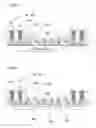
FIG. 6A shows: preparing a temporary carrier; applying a release layer 31 on top of the temporary carrier; and applying a bottom seed layer 32 on top of the release layer 31.
FIG. 6B shows: forming a redistribution layer RDL1 on top of the seed layer 32.
FIG. 6C shows: forming a seed layer 322 on top of the redistribution layer RDL1.
FIG. 6D shows: forming a patterned photo-resist PR on top of the seed layer 322.
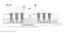
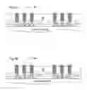
FIG. 6E shows a plurality of metal pillar 36 is formed in the periphery of the package unit.
FIG. 6F shows stripping the photo resist PR, and revealing the plurality of metal pillar 36;
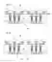
FIG. 6G shows applying a cylindrical molding compound 372 to encapsulate the plurality of metal pillar 36 to form a central cavity 388 in the center of the cylindrical molding compound 372.
FIG. 6H shows thinning from top of the molding compound 372, and revealing a top of each metal pillar 36.
FIG. 6I shows removing portion of the molding compound 372 from top, and revealing a top end of each metal pillar 36;
FIG. 6J shows forming a protection layer 361, such as an ENEPIG 362 on each revealed top of the metal pillar 36;
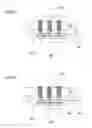
FIG. 6K shows planting a plurality of solder ball 38, each is planted on top of a corresponding ENEPIG 362 which brackets a top end of a corresponding metal pillar 36; mounting at least one passive element 395 such as a capacitor in the central cavity 388.
FIG. 6L shows removing the temporary carrier, removing the seed layer 32, and attaching at least one IC chip 391 from bottom of the package.
FIG. 6M shows a top view of FIG. 6H. FIG. 6I shows least a capacitor 395 is configured in the central cavity 388. The central cavity 388 is surrounded by the cylindrical molding compound 372.
The passive element 395 is configured near the bottom chip 391; the close distance shortens the circuit trace therebetween so that simultaneously switching noise (SSN) can be reduced to a minimum at a first stage when power is on for the IC package.
While several embodiments have been described by way of example, it will be apparent to those skilled in the art that various modifications may be configured without departs from the spirit of the present invention. Such modifications are all within the scope of the present invention, as defined by the appended claims.
Claims
1. A molding compound supported redistribution layer (RDL) structure for an integrated circuit (IC) package, the molding compound supported RDL structure comprising:
a molding compound;
a central cavity surrounded by the molding compound;
a plurality of metal pillars partially embedded in the molding compound, each metal pillar among the plurality of metal pillars having a bottom end protruded below the molding compound;
a redistribution layer having a plurality of bottom metal pads and a plurality of top metal pads; and
a chip mounted on bottom of the plurality of bottom metal pads,
wherein
a density of the plurality of bottom metal pads is higher than the density of the plurality of top metal pads;
the bottom end of each metal pillar among the plurality of metal pillars is electrically coupled to a corresponding top metal pad among the plurality of top metal pads;
at least one of the plurality of top metal pads is located in the central cavity and is configured for mounting at least one passive element; and
wherein, in a thickness direction of the RDL structure, the redistribution layer is arranged between the chip and the plurality of metal pillars.
2. A molding compound supported RDL structure as claimed in claim 1, further comprising:
a top protection layer bracketing a top end of a corresponding metal pillar among the plurality of metal pillars.
3. A molding compound supported RDL structure as claimed in claim 2, wherein the top protection layer is selected from the group consisting of Electroless Nickel/Electroless Palladium/Immersion Gold (ENEPIG) and Organic Solderability Preservatives (OSP).
4. A molding compound supported RDL structure as claimed in claim 2, further comprising:
a plurality of solder balls, each configured on top of the top protection layer bracketing the top end of a corresponding metal pillar among the plurality of metal pillars.
5. A molding compound supported RDL structure as claimed in claim 1, further comprising:
a plurality of solder balls, each directly configured on top of a corresponding metal pillar among the plurality of metal pillars.
6. A molding compound supported RDL structure as claimed in claim 4, further comprising:
a bottom protection layer configured on bottom of a corresponding bottom metal pad among the plurality of bottom metal pads.
7. A molding compound supported RDL structure as claimed in claim 6, wherein the bottom protection layer is selected from the group consisting of ENEPIG and OSP.
8. A molding compound supported RDL structure as claimed in claim 5, further comprising:
a bottom protection layer configured on bottom of a corresponding bottom metal pad among the plurality of bottom metal pads.
9. A molding compound supported RDL structure as claimed in claim 8, wherein the bottom protection layer is selected from the group consisting of ENEPIG and OSP.
10. A fabricating process for a molding compound supported redistribution layer (RDL) structure for an integrated circuit (IC) package, the fabricating process comprising:
applying a release layer on top of a temporary carrier;
applying a bottom seed layer on top of the releasing layer;
forming a redistribution layer on top of the bottom seed layer, the redistribution layer having a plurality of bottom metal pads and a plurality of top metal pads;
applying a top seed layer on top of the redistribution layer;
forming a patterned photo resist on top of the top seed layer;
forming a plurality of metal pillars, each on top of a corresponding top metal pad among the plurality of top metal pads;
stripping the patterned photo resist;
stripping the top seed layer between the plurality of metal pillars;
applying a molding compound to encapsulate the plurality of metal pillars and to form a central cavity in a center of the molding compound;
thinning the molding compound from top to expose top surfaces of the plurality of metal pillars; and
mounting a chip on bottom of the plurality of bottom metal pads,
wherein, in a thickness direction of the RDL structure, the redistribution layer is arranged between the chip and the plurality of metal pillars.
11. A fabricating process as claimed in claim 10, further comprising:
after said thinning, removing a portion of the molding compound from top to expose top ends of the plurality of metal pillars;
forming a protection layer bracketing the exposed top end of each metal pillar among the plurality of metal pillars;
planting a plurality of solder balls, each on top of the top protection layer which brackets the top end of a corresponding metal pillar among the plurality of metal pillars;
removing the temporary carrier; and
removing the bottom seed layer.
12. A fabricating process as claimed in claim 11, further comprising:
forming a bottom protection layer on bottom of a corresponding bottom metal pad among the plurality of bottom metal pads.
13. A fabricating process as claimed in claim 10, further comprising:
forming a protection layer bracketing the exposed top end of each metal pillar among the plurality of metal pillars;
planting a plurality of solder balls, each on top of the top protection layer which brackets the top end of a corresponding metal pillar among the plurality of metal pillars, wherein the top protection layer is cleaned out by soldering flux and heat and each of the plurality of solder balls is directly configured on top of a corresponding metal pillar among the plurality of metal pillars;
removing the temporary carrier; and
removing the bottom seed layer.
14. A fabricating process as claimed in claim 13, further comprising:
forming a bottom protection layer on bottom of a corresponding bottom metal pad among the plurality of bottom metal pads.
15. A fabricating process as claimed in claim 10, further comprising:
mounting at least one passive element over at least one of the plurality of top metal pads located in the central cavity,
wherein said chip is electrically connected to the at least one passive element by the redistribution layer arranged, in the thickness direction, between the chip and the at least one passive element.
16. A molding compound supported RDL structure as claimed in claim 1, further comprising:
at least one passive element mounted over said at least one of the plurality of top metal pads located in the central cavity,
wherein said chip is electrically connected to the at least one passive element by the redistribution layer arranged, in the thickness direction, between the chip and the at least one passive element.
17. (canceled)
18. (canceled)
19. A molding compound supported RDL structure as claimed in claim 16, wherein
the at least one passive element overlaps the chip in the thickness direction of the redistribution layer.
20. A molding compound supported RDL structure as claimed in claim 19, wherein
the molding compound has a topmost surface and a bottommost surface,
each metal pillar among the plurality of metal pillars extends from the topmost surface of the molding compound, through an entire thickness of the molding compound, to and further beyond the bottommost surface of the molding compound, and terminates at the bottom end protruded below the bottommost surface of the molding compound, and
the at least one passive element is co-elevational with the molding compound.
21. A molding compound supported RDL structure as claimed in claim 20, wherein
the at least one passive element comprises a plurality of passive elements arranged in the central cavity, and
adjacent passive elements among the plurality of passive elements have respective sidewalls physically spaced from each other.
22. A molding compound supported RDL structure as claimed in claim 1, wherein
the redistribution layer further comprises a topmost dielectric layer, and
the plurality of top metal pads and the bottom end of each metal pillar among the plurality of metal pillars are embedded in the topmost dielectric layer.
Images & Drawings included:


Sources:
- United States Patent and Trademark Office - verify current appl. status at the USPTO↗
Similar patent applications:
- » 20160118312
Molding compound supported RDL for IC package
Recent applications in this class:
- » 20250279348 2025-09-04
FINISHING ON PACKAGING SUBSTRATE WITH ULTRA HIGH-DENSITY INTERCONNECTS - » 20250266345 2025-08-21
METHODS AND APPARATUS TO REDUCE DISCOLORATION OF SOLDER RESISTS IN IMMERSION COOLING ENVIRONMENTS - » 20250259923 2025-08-14
POWER SEMICONDUCTOR MODULE ARRANGEMENT AND METHOD FOR PRODUCING THE SAME - » 20250253229 2025-08-07
CIRCUIT BOARD AND SEMICONDUCTOR PACKAGE COMPRISING SAME - » 20250226306 2025-07-10
ELECTRONIC DEVICE - » 20250218927 2025-07-03
FLAT PACKAGE - » 20250218926 2025-07-03
MICROELECTRONIC ASSEMBLIES INCLUDING CAVITY-LESS ENCAPSULATED DIES - » 20250132243 2025-04-24
SEMICONDUCTOR PACKAGE - » 20250112144 2025-04-03
INTEGRATED CIRCUIT PACKAGES INCLUDING A SUBSTRATE HAVING THERMAL ISOMERIC MOIETIES AND NON-THERMAL ISOMERIC MOIETIES - » 20250105133 2025-03-27
SEMICONDUCTOR PACKAGE INCLUDING INSULATING MATERIAL