Conductive organic semiconductor compound, method for preparing the same and organic thin-film transistor including the same
US20160149137A1
2016-05-26
14/659,809
2015-03-17
✅ Patent granted
US 9,941,476 B2
2018-04-10
-
-
John P Dulka
Goldilocks Zone IP Law
2035-12-23
Abstract:
The present disclosure provides an organic semiconductor compound, which has superior charge mobility, low band gap, wide light absorption area and adequate molecular energy level. The conductive organic semiconductor compound of the present disclosure can be used as a material for various organic optoelectric devices such as an organic photodiode (OPD), an organic light-emitting diode (OLED), an organic thin-film transistor (OTFT), an organic solar cell, etc. In addition, it can be prepared into a thin film via a solution process, can be advantageously used to fabricate large-area devices and can reduce the cost of device fabrication.
Inventors:
- Min-Jae KO 19 🇰🇷 Seoul, South Korea
- Hong-Gon KIM 33 🇰🇷 Seoul, South Korea
- Doh-Kwon LEE 31 🇰🇷 Seoul, South Korea
- Bong-Soo KIM 25 🇰🇷 Seoul, South Korea
- Jin Young KIM 184 🇰🇷 Seoul, South Korea
- Sungmin Park 33 🇰🇷 Seoul, South Korea
- Hae Jung SON 25 🇰🇷 Seoul, South Korea
Assignee:
- Korea Institute of Science and Technology 2,066 🇰🇷 Seoul, South Korea
Applicant:
Interested in similar patents?
Get notified when new applications in this technology area are published.
Classification:
H01L51/0043 » CPC further
Solid state devices using organic materials as the active part, or using a combination of organic materials with other materials as the active part; Processes or apparatus specially adapted for the manufacture or treatment of such devices, or of parts thereof; Selection of organic semiconducting materials, e.g. organic light sensitive or organic light emitting materials; Organic polymers or oligomers Copolymers
H01L51/0096 » CPC further
Solid state devices using organic materials as the active part, or using a combination of organic materials with other materials as the active part; Processes or apparatus specially adapted for the manufacture or treatment of such devices, or of parts thereof Substrates
H01L51/105 » CPC further
Solid state devices using organic materials as the active part, or using a combination of organic materials with other materials as the active part; Processes or apparatus specially adapted for the manufacture or treatment of such devices, or of parts thereof specially adapted for rectifying, amplifying, oscillating or switching, or capacitors or resistors with at least one potential- jump barrier or surface barrier multistep processes for their manufacture; Details of devices; Electrodes Ohmic contacts, e.g. source and drain electrodes
H01L51/055 » CPC further
Solid state devices using organic materials as the active part, or using a combination of organic materials with other materials as the active part; Processes or apparatus specially adapted for the manufacture or treatment of such devices, or of parts thereof specially adapted for rectifying, amplifying, oscillating or switching, or capacitors or resistors with at least one potential- jump barrier or surface barrier multistep processes for their manufacture the devices being controllable only by the electric current supplied or the electric potential applied, to an electrode which does not carry the current to be rectified, amplified or swiched, e.g. three-terminal devices; Field-effect devices, e.g. TFTs insulated gate field effect transistors characterised by the gate conductor
H01L51/0525 » CPC further
Solid state devices using organic materials as the active part, or using a combination of organic materials with other materials as the active part; Processes or apparatus specially adapted for the manufacture or treatment of such devices, or of parts thereof specially adapted for rectifying, amplifying, oscillating or switching, or capacitors or resistors with at least one potential- jump barrier or surface barrier multistep processes for their manufacture the devices being controllable only by the electric current supplied or the electric potential applied, to an electrode which does not carry the current to be rectified, amplified or swiched, e.g. three-terminal devices; Field-effect devices, e.g. TFTs insulated gate field effect transistors characterised by the gate dielectric the gate dielectric comprising only inorganic materials
H01L2251/308 » CPC further
Indexing scheme relating to organic semiconductor devices covered by group; Materials; Inorganic materials; Oxides, e.g. metal oxides; Transparent conductive oxides [TCO] composed of indium oxides, e.g. ITO
H01L2251/301 » CPC further
Indexing scheme relating to organic semiconductor devices covered by group; Materials Inorganic materials
H01L51/10 IPC
Solid state devices using organic materials as the active part, or using a combination of organic materials with other materials as the active part; Processes or apparatus specially adapted for the manufacture or treatment of such devices, or of parts thereof specially adapted for rectifying, amplifying, oscillating or switching, or capacitors or resistors with at least one potential- jump barrier or surface barrier multistep processes for their manufacture Details of devices
H01L51/0036 » CPC main
Solid state devices using organic materials as the active part, or using a combination of organic materials with other materials as the active part; Processes or apparatus specially adapted for the manufacture or treatment of such devices, or of parts thereof; Selection of organic semiconducting materials, e.g. organic light sensitive or organic light emitting materials; Organic polymers or oligomers comprising aromatic, heteroaromatic, or arrylic chains, e.g. polyaniline , polyphenylene , polyphenylene vinylene Heteroaromatic compounds comprising sulfur or selene, e.g. polythiophene
H01L51/0035 » CPC further
Solid state devices using organic materials as the active part, or using a combination of organic materials with other materials as the active part; Processes or apparatus specially adapted for the manufacture or treatment of such devices, or of parts thereof; Selection of organic semiconducting materials, e.g. organic light sensitive or organic light emitting materials; Organic polymers or oligomers comprising aromatic, heteroaromatic, or arrylic chains, e.g. polyaniline , polyphenylene , polyphenylene vinylene
C08G2261/592 » CPC further
Macromolecular compounds obtained by reactions forming a carbon-to-carbon link in the main chain of the macromolecule; Physical properties; Stability against heat
C08G61/123 » CPC further
Macromolecular compounds obtained by reactions forming a carbon-to-carbon link in the main chain of the macromolecule; Macromolecular compounds containing atoms other than carbon in the main chain of the macromolecule derived from five- or six-membered heterocyclic compounds, other than imides derived from five-membered heterocyclic compounds
C08G61/124 » CPC further
Macromolecular compounds obtained by reactions forming a carbon-to-carbon link in the main chain of the macromolecule; Macromolecular compounds containing atoms other than carbon in the main chain of the macromolecule derived from five- or six-membered heterocyclic compounds, other than imides derived from five-membered heterocyclic compounds with a five-membered ring containing one nitrogen atom in the ring
C08G61/126 » CPC further
Macromolecular compounds obtained by reactions forming a carbon-to-carbon link in the main chain of the macromolecule; Macromolecular compounds containing atoms other than carbon in the main chain of the macromolecule derived from five- or six-membered heterocyclic compounds, other than imides derived from five-membered heterocyclic compounds with a five-membered ring containing one sulfur atom in the ring
C08G2261/12 » CPC further
Macromolecular compounds obtained by reactions forming a carbon-to-carbon link in the main chain of the macromolecule; Definition of the polymer structure Copolymers
C08G2261/146 » CPC further
Macromolecular compounds obtained by reactions forming a carbon-to-carbon link in the main chain of the macromolecule; Definition of the polymer structure; Side-groups Side-chains containing halogens
C08G2261/1412 » CPC further
Macromolecular compounds obtained by reactions forming a carbon-to-carbon link in the main chain of the macromolecule; Definition of the polymer structure; Side-groups; Side-chains having aliphatic units Saturated aliphatic units
C08G2261/18 » CPC further
Macromolecular compounds obtained by reactions forming a carbon-to-carbon link in the main chain of the macromolecule; Definition of the polymer structure conjugated
C08G2261/3223 » CPC further
Macromolecular compounds obtained by reactions forming a carbon-to-carbon link in the main chain of the macromolecule; Monomer units or repeat units incorporating structural elements in the main chain incorporating heteroaromatic structural elements in the main chain non-condensed containing one or more sulfur atoms as the only heteroatom, e.g. thiophene
C08G2261/3229 » CPC further
Macromolecular compounds obtained by reactions forming a carbon-to-carbon link in the main chain of the macromolecule; Monomer units or repeat units incorporating structural elements in the main chain incorporating heteroaromatic structural elements in the main chain non-condensed containing nitrogen and sulfur as heteroatoms
C08G2261/3241 » CPC further
Macromolecular compounds obtained by reactions forming a carbon-to-carbon link in the main chain of the macromolecule; Monomer units or repeat units incorporating structural elements in the main chain incorporating heteroaromatic structural elements in the main chain condensed containing one or more nitrogen atoms as the only heteroatom, e.g. carbazole
C08G2261/3243 » CPC further
Macromolecular compounds obtained by reactions forming a carbon-to-carbon link in the main chain of the macromolecule; Monomer units or repeat units incorporating structural elements in the main chain incorporating heteroaromatic structural elements in the main chain condensed containing one or more sulfur atoms as the only heteroatom, e.g. benzothiophene
C08G2261/3245 » CPC further
Macromolecular compounds obtained by reactions forming a carbon-to-carbon link in the main chain of the macromolecule; Monomer units or repeat units incorporating structural elements in the main chain incorporating heteroaromatic structural elements in the main chain condensed containing nitrogen and oxygen as heteroatoms
C08G2261/3246 » CPC further
Macromolecular compounds obtained by reactions forming a carbon-to-carbon link in the main chain of the macromolecule; Monomer units or repeat units incorporating structural elements in the main chain incorporating heteroaromatic structural elements in the main chain condensed containing nitrogen and sulfur as heteroatoms
C08G2261/334 » CPC further
Macromolecular compounds obtained by reactions forming a carbon-to-carbon link in the main chain of the macromolecule; Monomer units or repeat units incorporating structural elements in the main chain incorporating non-aromatic structural elements in the main chain containing heteroatoms
C08G2261/344 » CPC further
Macromolecular compounds obtained by reactions forming a carbon-to-carbon link in the main chain of the macromolecule; Monomer units or repeat units incorporating structural elements in the main chain incorporating partially-aromatic structural elements in the main chain containing heteroatoms
C08G2261/364 » CPC further
Macromolecular compounds obtained by reactions forming a carbon-to-carbon link in the main chain of the macromolecule; Monomer units or repeat units incorporating structural elements in the main chain; Oligomers, i.e. comprising up to 10 repeat units containing hetero atoms
C08G2261/414 » CPC further
Macromolecular compounds obtained by reactions forming a carbon-to-carbon link in the main chain of the macromolecule; Polymerisation processes; Organometallic coupling reactions Stille reactions
C08G2261/92 » CPC further
Macromolecular compounds obtained by reactions forming a carbon-to-carbon link in the main chain of the macromolecule; Applications TFT applications
H01L51/0545 » CPC further
Solid state devices using organic materials as the active part, or using a combination of organic materials with other materials as the active part; Processes or apparatus specially adapted for the manufacture or treatment of such devices, or of parts thereof specially adapted for rectifying, amplifying, oscillating or switching, or capacitors or resistors with at least one potential- jump barrier or surface barrier multistep processes for their manufacture the devices being controllable only by the electric current supplied or the electric potential applied, to an electrode which does not carry the current to be rectified, amplified or swiched, e.g. three-terminal devices; Field-effect devices, e.g. TFTs insulated gate field effect transistors Lateral single gate single channel transistors with inverted structure, i.e. the organic semiconductor layer is formed after the gate electrode
H01L51/0558 » CPC further
Solid state devices using organic materials as the active part, or using a combination of organic materials with other materials as the active part; Processes or apparatus specially adapted for the manufacture or treatment of such devices, or of parts thereof specially adapted for rectifying, amplifying, oscillating or switching, or capacitors or resistors with at least one potential- jump barrier or surface barrier multistep processes for their manufacture the devices being controllable only by the electric current supplied or the electric potential applied, to an electrode which does not carry the current to be rectified, amplified or swiched, e.g. three-terminal devices; Field-effect devices, e.g. TFTs insulated gate field effect transistors characterised by the channel of the transistor
Y02E10/549 » CPC further
Energy generation through renewable energy sources; Photovoltaic [PV] energy Organic PV cells
Y02E10/549 » CPC further
Energy generation through renewable energy sources; Photovoltaic [PV] energy Organic PV cells
H01L51/00 IPC
Solid state devices using organic materials as the active part, or using a combination of organic materials with other materials as the active part; Processes or apparatus specially adapted for the manufacture or treatment of such devices, or of parts thereof
C08G61/12 IPC
Macromolecular compounds obtained by reactions forming a carbon-to-carbon link in the main chain of the macromolecule Macromolecular compounds containing atoms other than carbon in the main chain of the macromolecule
H01L51/05 IPC
Solid state devices using organic materials as the active part, or using a combination of organic materials with other materials as the active part; Processes or apparatus specially adapted for the manufacture or treatment of such devices, or of parts thereof specially adapted for rectifying, amplifying, oscillating or switching, or capacitors or resistors with at least one potential- jump barrier or surface barrier multistep processes for their manufacture
Description
CROSS-REFERENCE TO RELATED APPLICATIONS
This application claims priority under 35 U.S.C. §119 to Korean Patent Application No. 10-2014-0163341 filed on Nov. 21, 2014 in the Korean Intellectual Property Office, the disclosure of which is incorporated herein by reference in its entirety.
TECHNICAL FIELD
The present disclosure relates to a novel organic semiconductor compound containing difluorothiophene, more particularly to a new n-type organic semiconductor compound having high solubility and thermal stability, a method for preparing the same and various uses thereof.
BACKGROUND
The advent of organic semiconductors has enabled fabrication on a flexible plastic substrate and thus realization of a flexible display. Since it was reported that a conjugated polymer exhibits semiconductor properties and an electrical conductivity comparable to that of a metal can be achieved by doping it, the organic semiconductors are being developed more actively.
Recently, many researches are being conducted on organic light emitting diodes that can be used for various mobile electronic devices and on organic thin-film transistors wherein even the devices for driving the light emitting diodes are replaced by organic materials.
The organic thin-film transistor is advantageous over the thin-film transistor using amorphous silicon or polysilicon in that it can be fabricated at low cost via a simple process and is excellently compatible with plastic substrates used to fabricate flexible displays. In particular, when an organic semiconductor material with superior solubility is used, a thin film can be prepared easily via a solution process, which allows for preparation with large area at much lower cost.
The existing general organic thin-film transistor has a structure of substrate/gate electrode/insulating layer/electrode (source and drain) layers/organic semiconductor layer. A gate electrode is formed on a substrate, an insulating layer is formed on the gate electrode, and an organic semiconductor layer, a source electrode and a drain electrode are formed sequentially on the insulating layer. When an organic semiconductor is used as an n-type semiconductor in the organic thin-film transistor having such a structure, if a low voltage is applied between the source and drain electrodes, a current proportional to the applied voltage flows. At this time, if a negative voltage is applied to the gate electrode, electrons having negative charge are forced to the upper organic semiconductor layer due to the electric field formed by the voltage. As a result, a depletion layer without conductive charges is formed near the insulating layer. In this situation, even when a voltage is applied between the source and drain electrodes, the current is low because of decreased amount of conductive charge carriers. Conversely, if a positive voltage is applied to the gate electrode, a negatively charged accumulation layer is formed near the insulating layer due to the electric field formed by the applied voltage. In this case, a large current can flow because there are many conductive charge carriers between the source and drain electrodes. Accordingly, the current flowing between the source and drain electrodes can be controlled by alternatingly applying negative and positive voltages to the gate electrode in the state where a voltage is applied between the source and drain electrodes.
In the existing organic thin-film transistor including the n-type semiconductor operating based on the above-described principle, a substrate and source, drain and gate electrodes with high thermal stability, an insulator with high insulating property (dielectric constant) and an organic semiconductor that allows facile charge transport are required. To overcome the problems of the organic thin-film transistor, there are much to be improved for the materials of the insulator, organic semiconductor, etc. In particular, since the organic semiconductor is the key material, to overcome the problem of the organic semiconductor material will provide a good solution to the problem of the organic thin-film transistor.
Until now, there has been more development in the p-type organic semiconductor materials based on hole transport than that of the n-type semiconductor materials based on electron transport. It is because, since hole mobility is larger than electron mobility in most cases, the n-type organic semiconductor tends to exhibit lower performance and conductivity as compared to the p-type organic semiconductor. Since fullerene (C60), which is the representative n-type organic semiconductor material, has low LUMO energy, it can transport electrons well. It is reported that an electron mobility up to 6 cm2/V·s can be achieved in vacuum. However, if an n-type transistor device is fabricated using the fullerene organic semiconductor material via a solution process, the electron mobility is very low as about 2.8×10⁻² cm2/V·s (non-patent document 1).
Although an n-type polymer semiconductor having an electron mobility of 1 cm2/V·s was reported, the electron mobility is still far from commercialization (non-patent document 2). That is to say, there have been little development of a flexible, organic semiconductor material which has superior electron mobility and can be usefully used for a solution process.
To construct circuits such as a p-n junction diode, a bipolar transistor, a transducer, etc. using an organic material, the development of an n-type organic semiconductor material is necessary. Especially, the development of a novel n-type organic semiconductor material that can solve the problems of the existing art is necessary. A superior n-type organic semiconductor that can solve the above-described problems will be usefully applied not only in transistors but also as an electron acceptor material for organic thin-film solar cells.
REFERENCES OF THE RELATED ART
Non-Patent Documents
- Non-patent document 1. T. D. Anthopoulos, B. Singh, N. Marjanovic, N. S. Sariciftci, A. M. Ramil, H. Sitter, M. Colle, and D. M. de Leeuw, Appl. Phys. Lett., 89, 213504 (2006).
- Non-patent document 2. T. Lei, J.-H. Dou, X.-Y. Cao, J.-Y. Wang, J. Pei, Adv. Mater. 25, 6589 (2013); H, Yan1, Z, Chen1, Y, Zheng1, C, Newman1, J. R. Quinn1, F, Dotz, M, Kastler, A. Facchetti, Nature 457, 679 (2009).
SUMMARY
The present disclosure is directed to providing a conductive organic semiconductor compound having superior charge mobility, low band gap, wide light absorption area and adequate molecular energy level and a method for preparing the same.
The present disclosure is also directed to providing an organic semiconductor thin film and an organic thin-film transistor using the conductive organic semiconductor compound.
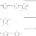
In an aspect, the present disclosure provides a conductive organic semiconductor compound represented by [Chemical Formula I] or [Chemical Formula II]:
In [Chemical Formula I] and [Chemical Formula II], Ar is selected from [Structural Formula 1]:
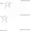
In [Structural Formula 1],
each of R1 and R2, which are identical or different, is independently selected from a group consisting of hydrogen, a halogen group, a cyano group, a nitro group, a hydroxyl group, an amide group, an ester group, a ketone group, a thioester group, a silyl group, a substituted or unsubstituted C1-C30 alkyl group, a substituted or unsubstituted C2-C30 alkenyl group, a substituted or unsubstituted C2-C30 alkynyl group, a substituted or unsubstituted C2-C50 heteroaryl group containing at least one of S, N, O, P and Si, a substituted or unsubstituted C3-C30 cycloalkyl group, a substituted or unsubstituted C3-C30 cycloalkenyl group, a substituted or unsubstituted C5-C50 aryl group, a substituted or unsubstituted C1-C30 alkoxy group, a substituted or unsubstituted C5-C50 aryloxy group, a substituted or unsubstituted C1-C30 alkylamino group, a substituted or unsubstituted C6-C30 arylamino group, a substituted or unsubstituted C1-C30 alkylsilyl group and a substituted or unsubstituted C5-C50 arylsilyl group, and
n is an integer from 5 to 100,000.
[Chemical Formula II] may be represented by [Chemical Formula III] or [Chemical Formula IV]:
In [Chemical Formula III] and [Chemical Formula IV],
each of R3 and R4, which are identical or different, is independently selected from a group consisting of hydrogen, a halogen group, a cyano group, a nitro group, a hydroxyl group, an amide group, an ester group, a ketone group, a thioester group, a silyl group, a substituted or unsubstituted C1-C30 alkyl group, a substituted or unsubstituted C2-C30 alkenyl group, a substituted or unsubstituted C2-C30 alkynyl group, a substituted or unsubstituted C2-C50 heteroaryl group containing at least one of S, N, O, P and Si, a substituted or unsubstituted C3-C30 cycloalkyl group, a substituted or unsubstituted C3-C30 cycloalkenyl group, a substituted or unsubstituted C5-C50 aryl group, a substituted or unsubstituted C1-C30 alkoxy group, a substituted or unsubstituted C5-C50 aryloxy group, a substituted or unsubstituted C1-C30 alkylamino group, a substituted or unsubstituted C6-C30 arylamino group, a substituted or unsubstituted C1-C30 alkylsilyl group and a substituted or unsubstituted C5-C50 arylsilyl group, and
n is an integer from 5 to 100,000.
[Chemical Formula III] may be represented by [Chemical Formula V]:
In [Chemical Formula V], n is an integer from 5 to 100,000.
[Chemical Formula IV] may be represented by [Chemical Formula VI]:
In [Chemical Formula VI], n is an integer from 5 to 100,000.
The conductive organic semiconductor compound may have an electron mobility of 1×10⁻⁶ cm2/V·s or higher.
The conductive organic semiconductor compound may have a band gap of 1.0-3.0 eV.
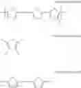
In another aspect, the present disclosure provides a method for preparing a conductive organic semiconductor compound represented by [Chemical Formula I], including dissolving a compound represented by [Chemical Formula VII] and a compound represented by [Chemical Formula VIII] in a solvent and causing them to react by adding a palladium catalyst:
In [Chemical Formula I], [Chemical Formula VII] and [Chemical Formula VIII], X is a halogen selected from Cl, Br and I, Y is selected from R6R7R8SnCl and BO2R9R10, and n is an integer from 5 to 100,000.
Each of R6, R7 and R8, which are identical or different, is hydrogen or a C1-C8 alkyl group, each of R9, R10, which are identical or different, is hydrogen or a C1-C8 alkyl group and the R9 and the R10 may be linked by a chemical bond.
Ar is the same as defined above in the description of the conductive organic semiconductor compound.
In another aspect, the present disclosure provides a method for preparing a conductive organic semiconductor compound represented by [Chemical Formula II], including dissolving a compound represented by [Chemical Formula VII] and a compound represented by [Chemical Formula IX] in a solvent and causing them to react by adding a palladium catalyst:
In [Chemical Formula II], [Chemical Formula VII] and [Chemical Formula IX], X is a halogen selected from Cl, Br and I, Y is selected from R6R7R8SnCl and BO2R9R10, and n is an integer from 5 to 100,000.
Each of R6, R7 and R8, which are identical or different, is hydrogen or a C1-C8 alkyl group, each of R9, R10, which are identical or different, is hydrogen or a C1-C8 alkyl group and the R9 and the R10 may be linked by a chemical bond.
Ar is the same as defined above in the description of the conductive organic semiconductor compound.
A molar mixing ratio of the compound represented by [Chemical Formula VII] and the compound represented by [Chemical Formula VIII] or [Chemical Formula IX] may be 1:0.5-2.
The solvent may be one or more selected from a group consisting of toluene, dimethylformamide, methanol, hexane, tri(o-tolyl)phosphine, chlorobenzene, ethylene acetate, tetrahydrofuran and N-methylpyrrolidinone.
The preparation method may be conducted at 100-200° C. for 10-60 hours.
In another aspect, the present disclosure provides an organic semiconductor thin film including one or more of the conductive organic semiconductor compound described above.
The conductive organic semiconductor compound may be prepared into a thin film by a method selected from a group consisting of vacuum deposition, screen printing, printing, spin coating, dipping and inkjet printing.
In another aspect, the present disclosure provides an organic thin-film transistor, including a substrate, a gate electrode formed on the substrate, an insulating layer formed on the gate electrode, the organic semiconductor thin film formed on the insulating layer, and a source electrode layer and a drain electrode layer formed on the organic semiconductor thin film.
The organic thin-film transistor may have a top-contact or bottom-contact structure.
The gate electrode, the source electrode and the drain electrode may be selected from a group consisting of gold, silver, aluminum, nickel, chromium and indium tin oxide.
The substrate may be selected from a group consisting of glass, polyethylene naphthalate, polyethylene terephthalate, polycarbonate, polyvinyl alcohol, polyacrylate, polyimide, polynorbornene and polyethersulfone.
The insulating layer may be selected from a group consisting of a ferroelectric insulator selected from a group consisting of Ba0.33Sr0.66TiO3 (BST), Al2O3, Ta2O5, La2O5, Y2O3 and TiO2, an inorganic insulator selected from a group consisting of PdZr0.33Ti0.66O3 (PZT), Bi4Ti3O12, BaMgF4, SrBi2(TaNb)2O9, Ba(ZrTi)O3(BZT), BaTiO3, SrTiO3, Bi4Ti3O12, SiO2, SiNx and AlON, polyimide, BCB, parylene, polyacrylate, polyvinyl alcohol and polyvinylphenol.
Since the conductive organic semiconductor compound according to the present disclosure has superior charge mobility, low band gap, wide light absorption area and adequate molecular energy level, it can be used as a material for various organic optoelectric devices such as an organic photodiode (OPD), an organic light-emitting diode (OLED), an organic thin-film transistor (OTFT), an organic solar cell, etc. In addition, it can be prepared into a thin film via a solution process, can be advantageously used to fabricate large-area devices and can reduce the cost of device fabrication.
BRIEF DESCRIPTION OF DRAWINGS
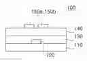
FIG. 1 is a cross-sectional view showing the structure of an organic thin-film transistor including a conductive organic semiconductor compound according to the present disclosure.
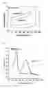
FIG. 2 shows the thermogravimetric analysis (TGA) result of a conductive organic semiconductor compound prepared in Synthesis Example 6 (PNDI2F3T) and a conductive organic semiconductor compound prepared in Synthesis Example 8 (PDPP2F3T).
FIG. 3 shows the differential scanning calorimetry (DSC) result of a conductive organic semiconductor compound prepared in Synthesis Example 6 (PNDI2F3T) and a conductive organic semiconductor compound prepared in Synthesis Example 8 (PDPP2F3T).
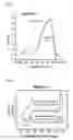
FIG. 4 shows the UV-vis absorption spectra of an organic semiconductor thin film prepared in Example 2 using a conductive organic semiconductor compound (PNDI2F3T, Synthesis Example 6) before and after annealing.
FIG. 5 shows the UV-vis absorption spectra of an organic semiconductor thin film prepared in Example 2 using a conductive organic semiconductor compound (PDPP2F3T, Synthesis Example 8) before and after annealing.
FIG. 6 shows the electrochemical properties of an organic semiconductor thin film prepared in Example 1 using a conductive organic semiconductor compound (PNDI2F3T, Synthesis Example 5 or 6) measured by cyclic voltammetry.
FIG. 7 shows the electrochemical properties of an organic semiconductor thin film prepared in Example 1 using a conductive organic semiconductor compound (PDPP2F3T, Synthesis Example 7 or 8) measured by cyclic voltammetry.
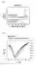
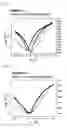
FIG. 8 shows the current-voltage (J-V) curve showing the electron mobility of an organic thin-film transistor prepared in Example 3 using a conductive organic semiconductor compound (PNDI2F3T, Synthesis Example 6). Gold was used as a top electrode of the organic thin-film transistor.
FIG. 9 shows the current-voltage (J-V) curve showing the electron mobility of an organic thin-film transistor prepared in Example 3 using a conductive organic semiconductor compound (PNDI2F3T, Synthesis Example 6). Aluminum was used as a top electrode of the organic thin-film transistor.
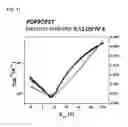
FIG. 10 shows the current-voltage (J-V) curve showing the electron mobility of an organic thin-film transistor prepared in Example 3 using a conductive organic semiconductor compound (PDPP2F3T, Synthesis Example 8). Gold was used as a top electrode of the organic thin-film transistor.
FIG. 11 shows the current-voltage (J-V) curve showing the electron mobility of an organic thin-film transistor prepared in Example 3 using a conductive organic semiconductor compound (PDPP2F3T, Synthesis Example 8). Aluminum was used as a top electrode of the organic thin-film transistor.
DETAILED DESCRIPTION OF EMBODIMENTS
Hereinafter, various aspects and exemplary embodiments of the present disclosure are described in further detail.
In an aspect, the present disclosure provides a conductive organic semiconductor compound represented by [Chemical Formula I] or [Chemical Formula II]:
In [Chemical Formula I] and [Chemical Formula II], Ar is selected from [Structural Formula 1]:
In [Structural Formula 1],
each of R1 and R2, which are identical or different, is independently selected from a group consisting of hydrogen, a halogen group, a cyano group, a nitro group, a hydroxyl group, an amide group, an ester group, a ketone group, a thioester group, a silyl group, a substituted or unsubstituted C1-C30 alkyl group, a substituted or unsubstituted C2-C30 alkenyl group, a substituted or unsubstituted C2-C30 alkynyl group, a substituted or unsubstituted C2-C50 heteroaryl group containing at least one of S, N, O, P and Si, a substituted or unsubstituted C3-C30 cycloalkyl group, a substituted or unsubstituted C3-C30 cycloalkenyl group, a substituted or unsubstituted C5-C50 aryl group, a substituted or unsubstituted C1-C30 alkoxy group, a substituted or unsubstituted C5-C50 aryloxy group, a substituted or unsubstituted C1-C30 alkylamino group, a substituted or unsubstituted C6-C30 arylamino group, a substituted or unsubstituted C1-C30 alkylsilyl group and a substituted or unsubstituted C5-C50 arylsilyl group, and
n is an integer from 5 to 100,000.
The conductive organic semiconductor compound represented by [Chemical Formula II] may be represented by [Chemical Formula III] or [Chemical Formula IV]:
In [Chemical Formula III] and [Chemical Formula IV],
each of R3 and R4, which are identical or different, is independently selected from a group consisting of hydrogen, a halogen group, a cyano group, a nitro group, a hydroxyl group, an amide group, an ester group, a ketone group, a thioester group, a silyl group, a substituted or unsubstituted C1-C30 alkyl group, a substituted or unsubstituted C2-C30 alkenyl group, a substituted or unsubstituted C2-C30 alkynyl group, a substituted or unsubstituted C2-C50 heteroaryl group containing at least one of S, N, O, P and Si, a substituted or unsubstituted C3-C30 cycloalkyl group, a substituted or unsubstituted C3-C30 cycloalkenyl group, a substituted or unsubstituted C5-C50 aryl group, a substituted or unsubstituted C1-C30 alkoxy group, a substituted or unsubstituted C5-C50 aryloxy group, a substituted or unsubstituted C1-C30 alkylamino group, a substituted or unsubstituted C6-C30 arylamino group, a substituted or unsubstituted C1-C30 alkylsilyl group and a substituted or unsubstituted C5-C50 arylsilyl group, and
n is an integer from 5 to 100,000.
The conductive organic semiconductor compound represented by [Chemical Formula III] may be represented by [Chemical Formula V]:
In [Chemical Formula V], n is an integer from 5 to 100,000.
The conductive organic semiconductor compound represented by [Chemical Formula IV] may be represented by [Chemical Formula VI]:
In [Chemical Formula VI], n is an integer from 5 to 100,000.
Since the conductive organic semiconductor compound has a number average molecular weight (Mn) of about 10,000-100,000, it can be controlled to have superior solubility for various organic solvents. Accordingly, it can be prepared into a thin film with superior crystallinity in various organic solvents.
In particular, since the conductive organic semiconductor compound has high a repeat unit having a thiophene monomer and a dipyrrolopyrrole monomer with high hole mobility and superior light absorption ability and a dithienobenzodithiophene core with excellent hole conductivity, it has low band gap and exhibits high charge mobility and low cutoff current loss when used as an organic semiconductor of a transistor.
The conductive organic semiconductor compound may have an electron mobility of 1×10⁻⁶ cm2/V·s or higher.
Since the conductive organic semiconductor compound has a low band gap of 1.0-3.0 eV, it can be usefully used as a material for an organic optoelectric device selected from an organic photodiode, an organic light-emitting diode, an organic thin-film transistor and an organic solar cell.
The conductive organic semiconductor compound may be an n-type organic semiconductor compound.
In another aspect, the present disclosure provides a method for preparing a conductive organic semiconductor compound represented by [Chemical Formula I], including dissolving a compound represented by [Chemical Formula VII] and a compound represented by [Chemical Formula VIII] in a solvent and causing them to react by adding a palladium catalyst:
In [Chemical Formula I], [Chemical Formula VII] and [Chemical Formula VIII], X is a halogen selected from Cl, Br and I, Y is selected from R6R7R8SnCl and BO2R9R10, and n is an integer from 5 to 100,000.
Each of R6, R7 and R8, which are identical or different, is hydrogen or a C1-C8 alkyl group, each of R9, R10, which are identical or different, is hydrogen or a C1-C8 alkyl group and the R9 and the R10 may be linked by a chemical bond.
Ar is selected from [Structural Formula 1]:
In [Structural Formula 1],
each of R1 and R2, which are identical or different, is independently selected from a group consisting of hydrogen, a halogen group, a cyano group, a nitro group, a hydroxyl group, an amide group, an ester group, a ketone group, a thioester group, a silyl group, a substituted or unsubstituted C1-C30 alkyl group, a substituted or unsubstituted C2-C30 alkenyl group, a substituted or unsubstituted C2-C30 alkynyl group, a substituted or unsubstituted C2-C50 heteroaryl group containing at least one of S, N, O, P and Si, a substituted or unsubstituted C3-C30 cycloalkyl group, a substituted or unsubstituted C3-C30 cycloalkenyl group, a substituted or unsubstituted C5-C50 aryl group, a substituted or unsubstituted C1-C30 alkoxy group, a substituted or unsubstituted C5-C50 aryloxy group, a substituted or unsubstituted C1-C30 alkylamino group, a substituted or unsubstituted C6-C30 arylamino group, a substituted or unsubstituted C1-C30 alkylsilyl group and a substituted or unsubstituted C5-C50 arylsilyl group, and
n is an integer from 5 to 100,000.
In another aspect, the present disclosure provides a method for preparing a conductive organic semiconductor compound represented by [Chemical Formula II], including dissolving a compound represented by [Chemical Formula VII] and a compound represented by [Chemical Formula IX] in a solvent and causing them to react by adding a palladium catalyst:
In [Chemical Formula II], [Chemical Formula VII] and [Chemical Formula IX], X is a halogen selected from Cl, Br and I, Y is selected from R6R7R8SnCl and BO2R9R10, and n is an integer from 5 to 100,000.
Each of R6, R7 and R8, which are identical or different, is hydrogen or a C1-C8 alkyl group, each of R9, R10, which are identical or different, is hydrogen or a C1-C8 alkyl group and the R9 and the R10 may be linked by a chemical bond.
Ar is the same as defined above in the description of the method for preparing a conductive organic semiconductor compound represented by [Chemical Formula I].
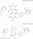
In the methods for preparing a conductive organic semiconductor compound represented by [Chemical Formula I] and a conductive organic semiconductor compound represented by [Chemical Formula II], the palladium catalyst may be a palladium(0) catalyst such as tetrakis(triphenylphosphine)palladium(0) (Pd(PPh3)4) or a palladium(II) catalyst such as 1,4-bis(triphenylphosphine)palladium(II) dichloride (PdCl2(PPh3)2), [1,4-bis(diphenylphosphine)butane]palladium(II) dichloride (Pd(dppb)Cl2), [1,1′-bis(diphenylphosphino)ferrocene]palladium(II) dichloride (Pd(dppf)Cl2) or palladium(II) acetate (Pd(OAc)2).
The content of the catalyst may be controlled depending on the monomers. For example, the tetrakis(triphenylphosphine)palladium compound may be used in an amount of 5-20 parts by weight based on 100 parts by weight of the monomer represented by [Chemical Formula VII].
In the preparation method, the solvent may be one or more selected from a group consisting of toluene, dimethylformamide, methanol, hexane, tri(o-tolyl)phosphine, chlorobenzene, ethylene acetate, tetrahydrofuran and N-methylpyrrolidinone.
The preparation method may be performed at 100-200° C. for 10-60 hours, more specifically at 100-140° C. for 20-40 hours.
The conductive organic semiconductor compound may be prepared into an organic semiconductor thin film. The organic semiconductor thin film may be prepared by a method selected from vacuum deposition, screen printing, printing, spin coating, dipping and inkjet printing.
Since the conductive organic semiconductor compound can be prepared into a thin film via a solution process, a large-area thin film can be prepared easily at low cost.
FIG. 1 is a cross-sectional view showing the structure of an organic thin-film transistor including a conductive organic semiconductor compound according to the present disclosure.
Referring to FIG. 1, the organic thin-film transistor 100 includes: a substrate 110; a gate electrode 120 formed on the substrate 110; an insulating layer 130 formed on the gate electrode 120; an organic semiconductor thin film 140 formed on the insulating layer 130; and a source electrode layer and a drain electrode layer 150a, 150b formed on the organic semiconductor thin film 140.
The substrate 110 may be formed of an inorganic material, an organic material or a composite of an inorganic material and an organic material. Specifically, it may be selected from a group consisting of glass, polyethylene naphthalate, polyethylene terephthalate, polycarbonate, polyvinyl alcohol, polyacrylate, polyimide, polynorbornene and polyethersulfone, although not being limited thereto.
The gate electrode 120 and the source electrode layer and the drain electrode layer 150a, 150b may be formed of a commonly used metal. Specifically, it may be selected from a group consisting of gold, silver, aluminum, nickel, chromium and indium tin oxide, although not being limited thereto.
The insulating layer 130 may be formed of a commonly used insulator with a high dielectric constant. Specifically, it may be selected from a group consisting of ferroelectric insulator selected from a group consisting of Ba0.33Sr0.66TiO3 (BST), Al2O3, Ta2O5, La2O5, Y2O3 and TiO2, an inorganic insulator selected from a group consisting of PdZr0.33Ti0.66O3 (PZT), Bi4Ti3O12, BaMgF4, SrBi2(TaNb)2O9, Ba(ZrTi)O3(BZT), BaTiO3, SrTiO3, Bi4Ti3O12, SiO2, SiNx and AlON, polyimide, BCB, parylene, polyacrylate, polyvinyl alcohol and polyvinylphenol, although not being limited thereto.
Specifically, the organic semiconductor thin film 140 may be an organic semiconductor thin film prepared from the conductive organic semiconductor compound represented by [Chemical Formula I] or the conductive organic semiconductor compound represented by [Chemical Formula II] described above. A description about the conductive organic semiconductor compounds will be omitted since it is the same as above.
Since the conductive organic semiconductor compound has excellent properties such as superior solubility and flexibility and low band gap, it can be used not only for the organic thin-film transistor but also for various memory devices, organic light-emitting diodes, photosensors, laser devices or photovoltaic devices such as an organic solar cell.
In particular, an organic solar cell prepared using the conductive organic semiconductor compound is advantageous in that the quantum yield is about 4 times or higher than that of the existing solar cell and the process cost is much lower.
Hereinafter, the present disclosure will be described in more detail through examples. However, the scope and content of the present disclosure cannot interpreted as being reduced or limited by the examples. In addition, it will be obvious that various changes and modifications can be easily made by those of ordinary skill in the art based on the present disclosure including the examples and that those changes and modifications are included in the scope of the appended claims.
EXAMPLES
Synthesis Examples
Synthesis of Conductive Organic Semiconductor Compound According to the Present Disclosure
Synthesis Example 1
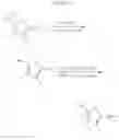
Synthesis of 2,5-dibromo-3,4-difluoro-thiophene (Chemical Formula 2)
A compound of Chemical Formula 1 (2.28 g, 8.62 mmol) and dichloromethane (10 mL) were added to a 100-mL flask containing a magnetic stirring bar. After cooling to 0° C., bromine (0.97 mL, 18.96 mmol) was slowly added dropwise. After slowly raising temperature to 50° C., reaction was performed for 3 hours. Then, after removing the remaining bromine with sodium bisulfite, followed by extraction with dichloromethane, the organic layer was dehydrated with magnesium sulfate. After removing the solvent using a rotary evaporator, followed by purification by column chromatography (hexane), 2,5-dibromo-3,4-difluoro-thiophene (Chemical Formula 2) (1.5 g, 62.6%) was obtained.
13C NMR (100 MHz, CDCl3): δ 90.33, 143.95.
Synthesis Example 2
Synthesis of 3,4-difluoro-2,5-bis-trimethylstannyl-thiophene (Chemical Formula 3)
The compound of Chemical Formula 2 (1.22 g, 4.39 mmol) and anhydrous tetrahydrofuran (18 mL) were added to a 100-mL flask containing a magnetic stirring bar under argon atmosphere. After cooling to −78° C., 1.6 M n-butyllithium (5.77 mL, 9.23 mmol) was slowly added dropwise. After maintaining at −78° C. for 40 minutes, followed by addition of a trimethyltin chloride solution (21.98 mL, 21.98 mmol, 1 M), reaction was performed for 12 hours at room temperature with stirring. After extracting with water and diethyl ether, the organic layer was dehydrated with magnesium sulfate. After removing the solvent using a rotary evaporator, followed by recrystallization in methanol at low temperature, 3,4-difluoro-2,5-bis-trimethylstannyl-thiophene (Chemical Formula 3) (786.2 mg, 40.1%) was obtained.
1H NMR (400 MHz, CDCl3): δ 0.39 (s, 12H).
Synthesis Example 3
Synthesis of N,N′-bis(2-decyltetradecyl)-2,6-di(thiophen-2-yl)naphthalene-1,4,5,8-bis(dicarboximide) (Chemical Formula 5)
The compound of Chemical Formula 4 (302.2 mg, 0.275 mmol), 2-tributylstannylthiophene (0.262 mL, 0.825 mmol) and tetrakis(triphenylphosphine)palladium(0) (Pd(PPh3)4) (15.9 mg, 0.014 mmol) were added to a 10-mL flask containing a magnetic stirring bar. Then, degassed toluene (4.8 mL) and dimethylformamide (1.2 mL) were added as solvents. After performing reaction at 120° C. for about 12 hours, the reaction mixture was cooled to room temperature, diluted with dichloromethane and washed 3 times with water and brine. The organic layer was dehydrated with magnesium sulfate and the solvent was removed using a rotary evaporator. After separation by column chromatography (dichloromethane:hexane=1:1), N,N′-bis(2-decyltetradecyl)-2,6-di(thiophen-2-yl)naphthalene-1,4,5,8-bis(dicarboximide) (Chemical Formula 5) (249.8 mg, 82.3%) was obtained.
1H NMR (400 MHz, CDCl3): δ 0.82-0.89 (m, 12H), 1.10-1.45 (m, 80H), 1.83-2.10 (br, 2H), 4.07 (d, 4H), 7.20 (d, 2H), 7.31 (d, 2H), 7.60 (d, 2H), 8.75 (s, 2H).
Synthesis Example 4
Synthesis of N,N′-bis(2-decyltetradecyl)-2,6-bis(5-bromothiophen-2-yl)naphthalene-1,4,5,8-bis(dicarboximide) (Chemical Formula 6)
The compound of Chemical Formula 5 (249.8 mg, 0.226 mmol), chloroform (8 mL) and dimethylformamide (2 mL) were added to a 25-mL flask containing a magnetic stirring bar. Then, a solution of N-bromosuccinimide (NBS) (96.7 mg, 0.543 mmol) dissolved in chloroform (2 mL) and dimethylformamide (3 mL) was slowly added dropwise. After covering with aluminum foil to prevent exposure to light and performing reaction at room temperature for 2 days, the solvent was removed using a rotary evaporator. After separation by column chromatography (dichloromethane:hexane=1:2), N,N′-bis(2-decyltetradecyl)-2,6-bis(5-bromothiophen-2-yl)naphthalene-1,4,5,8-bis(dicarboximide) (Chemical Formula 6) (205 mg, 71.9%) was obtained.
1H NMR (400 MHz, CDCl3): δ 0.79-0.92 (m, 12H), 1.10-1.43 (m, 80H), 1.83-2.01 (m, 2H), 4.06 (d, 4H), 7.08 (d, 2H), 7.14 (d, 2H), 8.71 (s, 2H).
Synthesis Example 5
Synthesis of PNDI2F3T (Chemical Formula V) (Synthesis Method 1)
The 3,4-difluoro-2,5-bis-trimethylstannyl-thiophene (Chemical Formula 3) (35.7 mg, 0.08 mmol) obtained in Synthesis Example 2, the N,N′-bis(2-decyltetradecyl)-2,6-bis(5-bromothiophen-2-yl)naphthalene-1,4,5,8-bis(dicarboximide) (Chemical Formula 6) (101 mg, 0.08 mmol) obtained in Synthesis Example 4 and tetrakis(triphenylphosphine)palladium(0) (Pd(PPh3)4) (3.9 mg, 3.44 μmol) were added to a 5-mL flask containing a magnetic stirring bar. Then, degassed toluene (1.3 mL) and dimethylformamide (0.3 mL) were added as solvents. After performing reaction at 120° C. for about 36 hours, the reaction mixture was cooled to room temperature, reprecipitated in methanol (50 mL) and then filtered. The reaction mixture was Soxhlet extracted with hexane and methanol and then with chloroform. The extracted solution was passed through a celite filter and the solvent was removed using a rotary evaporator. After reprecipitation in methanol (50 mL), a polymer PNDI2F3T (Chemical Formula V) (62 mg, 63.5%) was obtained.
GPC: Mn=13.5 kg/mol; PDI=1.53.
Synthesis Example 6
Synthesis of PNDI2F3T (Chemical Formula V) (Synthesis Method 2)
The 3,4-difluoro-2,5-bis-trimethylstannyl-thiophene (Chemical Formula 3) (35.5 mg, 0.08 mmol) obtained in Synthesis Example 2, the N,N′-bis(2-decyltetradecyl)-2,6-bis(5-bromothiophen-2-yl)naphthalene-1,4,5,8-bis(dicarboximide) (Chemical Formula 6) (100.4 mg, 0.08 mmol) obtained in Synthesis Example 4, tris(dibenzylideneacetone)dipalladium(0) (Pd2[dba]3) (1.5 mg, 1.6 μmol) and tri(o-tolyl)phosphine (1.9 mg, 6.4 μmol) were added to a 5-mL flask containing a magnetic stirring bar. Then, degassed chlorobenzene (1.6 mL) was added as a solvent. After performing reaction at 120° C. for about 36 hours, the reaction mixture was cooled to room temperature, reprecipitated in methanol (50 mL) and then filtered. The reaction mixture was Soxhlet extracted with hexane and methanol and then with chloroform. The extracted solution was passed through a celite filter and the solvent was removed using a rotary evaporator. After reprecipitation in methanol (50 mL), a polymer PNDI2F3T (Chemical Formula V) (82.5 mg, 85.0%) was obtained.
GPC: Mn=24.7 kg/mol; PDI=1.83.
Synthesis Example 7
Synthesis of PDPP2F3T (Chemical Formula VI) (Synthesis Method 1)
The 3,4-difluoro-2,5-bis-trimethylstannyl-thiophene (Chemical Formula 3) (53.6 mg, 0.12 mmol) obtained in Synthesis Example 2, 3,6-bis(5-bromothiophen-2-yl)-2,5-bis(2-decyltetradecyl)pyrrolo[3,4-c]pyrrole-1,4(2H,5H)-dione (Chemical Formula 7) (136.1 mg, 0.12 mmol) and tetrakis(triphenylphosphine)palladium(0) (Pd(PPh3)4) (6.0 mg, 5.17 μmol) were added to a 5-mL flask containing a magnetic stirring bar. Then, degassed toluene (1.9 mL) and dimethylformamide (0.5 mL) were added as solvents. After performing reaction at 120° C. for about 36 hours, the reaction mixture was cooled to room temperature, reprecipitated in methanol (50 mL) and then filtered. The reaction mixture was Soxhlet extracted with methanol, acetone and ethylene acetate and then with chloroform. The extracted solution was passed through a celite filter and the solvent was removed using a rotary evaporator. After reprecipitation in methanol (50 mL), a polymer PDPP2F3T (Chemical Formula VI) (90 mg, 68.8%) was obtained.
GPC: Mn=26.8 kg/mol; PDI=2.98.
Synthesis Example 8
Synthesis of PDPP2F3T (Chemical Formula VI) (Synthesis Method 2)
The 3,4-difluoro-2,5-bis-trimethylstannyl-thiophene (Chemical Formula 3) (50.8 mg, 0.114 mmol) obtained in Synthesis Example 2, 3,6-bis(5-bromothiophen-2-yl)-2,5-bis(2-decyltetradecyl)pyrrolo[3,4-c]pyrrole-1,4(2H,5H)-dione (Chemical Formula 7) (129.0 mg, 0.114 mmol), tris(dibenzylideneacetone)dipalladium(0) (Pd2[dba]3) (2.1 mg, 2.3 μmol) and tri(o-tolyl)phosphine (2.8 mg, 9.1 μmol) were added to a 5-mL flask containing a magnetic stirring bar. Then, degassed chlorobenzene (2.3 mL) was added as a solvent. After performing reaction at 120° C. for about 36 hours, the reaction mixture was cooled to room temperature, reprecipitated in methanol (50 mL) and then filtered. The reaction mixture was Soxhlet extracted with methanol and ethylene acetate and then with chloroform. The extracted solution was passed through a celite filter and the solvent was removed using a rotary evaporator. After reprecipitation in methanol (50 mL), a polymer PDPP2F3T (Chemical Formula VI) (108.9 mg, 87.7%) was obtained.
GPC: Mn=39.8 kg/mol; PDI=2.76.
Example 1
Preparation of Organic Semiconductor Thin Film
A glass substrate was prepared by drying after washing in isopropyl alcohol for 10 minutes, in acetone for 10 minutes and then in isopropyl alcohol for 10 minutes.
Then, a solution obtained by dissolving the conductive organic semiconductor compound (10 mg) prepared in Synthesis Example 5, 6, 7 or 8 in 1 mL of chlorobenzene was spin coated on the glass substrate at 1000 rpm to obtain each organic semiconductor thin film. Subsequently, the thin film was annealed at 200° C.
Example 2
Analysis of Electrical Properties of Conductive Organic Semiconductor Material
The electrochemical properties of the organic semiconductor thin film prepared in Example 1 was analyzed by cyclic voltammetry and its energy level was calculated.
Cyclic voltammetry measurement was made as follows. First, the organic semiconductor thin film (Example 1) coated on a carbon glass electrode was prepared as a working electrode, a platinum wire was prepared as a counter electrode and Ag/Ag+ was prepared as a reference electrode. A voltage was applied to the reference electrode (Ag/Ag+) using a potentiometer and the current flowing as a result of redox reaction of the analyte below the working electrode was measured at the counter electrode. The measured current was corrected for redox potential measurement using ferrocene/ferrocenium (Fc/Fc+) under the same condition. The redox potential of ferrocene/ferrocenium (Fc/Fc+) was 0.09 eV higher than that of the Ag/Ag+ electrode. The voltage when oxidation started ((pox) and the voltage (φred) when reduction started were measured and the highest occupied molecular orbital (HOMO) energy level and the lowest unoccupied molecular orbital (LUMO) energy level were calculated according to Equation 1.
EHOMO=−4.8(ΦOX−0.09)(eV)
ELUMO=−4.8(Φred−0.09)(eV) Equation 1
Example 3
Fabrication of Organic Thin-Film Transistor Using Conductive Organic Semiconductor Material
A transistor having a top-contact structure was fabricated using the conductive organic semiconductor compounds synthesized in Synthesis Examples 6 and 8 (PNDI2F3T, PDPP2F3T). The structure is shown in detail in FIG. 1.
To fabricate the transistor, first, a 300-nm thick silicon oxide film was formed on a heavily p-doped silicon gate electrode as insulating layer. Subsequently, a 20-nm thick Cytop™ thin film was formed on the insulating layer by spin coating and then a zirconium oxide film was formed by spin coating a solution of zirconium(IV) acetylacetonate (Zr(acac)4) dissolved in DMF via a sol-gel process. After annealing at 200° C. for an hour, a 40-nm thick polymer thin film was formed by spin coating a 0.2 wt % solution of the polymer dissolved in chloroform. Then, gold or aluminum was deposited to a thickness of 60 nm to form source and drain electrodes.
Test Example 1
Thermal Properties of Conductive Organic Semiconductor Compound
FIG. 2 shows the thermogravimetric analysis (TGA) result of the conductive organic semiconductor compound prepared in Synthesis Example 6 (PNDI2F3T) and the conductive organic semiconductor compound prepared in Synthesis Example 8 (PDPP2F3T). And, FIG. 3 shows the differential scanning calorimetry (DSC) result of the conductive organic semiconductor compound prepared in Synthesis Example 6 (PNDI2F3T) and the conductive organic semiconductor compound prepared in Synthesis Example 8 (PDPP2F3T).
As seen from FIG. 2 and FIG. 3, the conductive organic semiconductor compounds according to the present disclosure have superior thermal stability with high glass transition temperatures (Tg) above 400° C. (initial decomposition temperatures: 418° C. and 457° C., respectively). Accordingly, they can exhibit long life time when used as materials for an organic optoelectric device and can exhibit superior process stability when thermal deposition is necessary.
Test Example 2
Optical Properties of Conductive Organic Semiconductor Compound
FIG. 4 shows the UV-vis absorption spectra of the organic semiconductor thin film prepared in Example 2 using the conductive organic semiconductor compound (PNDI2F3T, Synthesis Example 6) before and after annealing. And, FIG. 5 shows the UV-vis absorption spectra of the organic semiconductor thin film prepared in Example 2 using the conductive organic semiconductor compound (PDPP2F3T, Synthesis Example 8) before and after annealing. In FIG. 4 and FIG. 5, the organic semiconductor thin film before the annealing was denoted as pristine film and the organic semiconductor thin film after the annealing was denoted as annealed film.
The maximum absorption wavelength (λmax), onset absorption wavelength (λonset) and optical band gap (Eg,opt) of the organic semiconductor thin film prepared in Example 2 using the conductive organic semiconductor compound (PNDI2F3T, Synthesis Example 6; PDPP2F3T, Synthesis Example 8) measured after the annealing are described in [Table 1].
| TABLE 1 | |||
| Maximum absorption | Onset absorption | Optical band | |
| wavelength (λmax) | wavelength (λonset) | gap (Eg,opt) | |
| PNDI2F3T | 407, 680 nm | 829 nm | 1.50 eV |
| (Synthesis | |||
| Example 6) | |||
| PDPP2F3T | 850 nm | 940 nm | 1.32 eV |
| (Synthesis | |||
| Example 8) | |||
As seen from FIG. 4, FIG. 5 and Table 1, the organic semiconductor thin films prepared from the conductive organic semiconductor compounds according to the present disclosure had low band gaps required for organic solar cells. This suggests that the conductive organic semiconductor compound of the present disclosure can be used to prepare a high-efficiency organic solar cell.
Test Example 3
Characteristics of Organic Thin-Film Transistor
After measuring the drain voltage-drain current vs. gate voltage and the gate voltage-drain current vs. drain voltage using the Keithley 2400 source/measure units, the characteristics of the fabricated device in the saturation regime were evaluated according to the following equation.
I d s = W C i 2 L μ ( V g s - V T ) 2 Equation 2
In Equation 2, VT is the threshold voltage, Vgs is the applied gate voltage, μ is the field-effect charge mobility, W and L are the channel width and length, and C is the capacitance of the insulating layer. The threshold voltage is determined by the gate voltage when Ids is 0 from the graph of √{square root over (Ids)} vs. Vgs, and the field-effect charge mobility is calculated from the slope of the √{square root over (Ids)} vs. Vgs curve.
FIGS. 8 and 9 show the current-voltage (J-V) curves showing the electron mobility of the organic thin-film transistors prepared in Example 3 using the conductive organic semiconductor compound (PNDI2F3T, Synthesis Example 6). Gold or aluminum was used as the top electrode of the organic thin-film transistors, respectively.
FIGS. 10 and 11 show the current-voltage (J-V) curves showing the electron mobility of the organic thin-film transistors prepared in Example 3 using the conductive organic semiconductor compound (PDPP2F3T, Synthesis Example 8). Gold or aluminum was used as the top electrode of the organic thin-film transistors, respectively.
The performance of the organic thin-film transistors is described in more detail in Table 2.
| TABLE 2 | |||
| Mobility | |||
| Condition | (cm2/Vs) | Ion/off | |
| PNDI2F3T (Synthesis | Au electrode | 0.19 | |
| Example 6) | Al electrode | 0.25 | |
| PDPP2F3T (Synthesis | Au electrode | 0.1 | |
| Example 8) | Al electrode | 0.13 | |
| Existing transistor | Adv. Funct. Mater. 2013, | 0.01 | — |
| [Comparative | 24, 1151-1162 | ||
| Example 1] | |||
| Existing transistor | Adv. Funct. Mater. 2013, | 6.5 × 10⁻⁴ | — |
| [Comparative | 24, 1151-1162 | ||
| Example 2] | |||
| Existing transistor | Chem. Mater., 2013, 25, | 0.05 | 104-105 |
| [Comparative | 2178-2183 | ||
| Example 3] | |||
As seen from Table 2, the transistors using the organic semiconductor thin films (i.e., the conductive organic semiconductor compounds) of the present disclosure exhibit significantly improved performance as compared to the transistors using the existing conductive organic semiconductor compounds. For example, the polymers wherein fluorine-free thiophene was introduced instead of difluorothiophene to the PNDI2F3T (Synthesis Example 6) of the present disclosure (Comparative Example 1 and Comparative Example 2) showed charge mobility of 0.01 cm2/Vs and 6.5×10⁻⁴ cm2/Vs, and the polymer wherein 2,1,3-benzothiadiazole was introduced instead of difluorothiophene showed charge mobility of 0.05 cm2/Vs. In contrast, the polymer organic semiconductors according to the present disclosure showed 4 to tens of times increased charge mobility.
Claims
What is claimed is:1. A conductive organic semiconductor compound represented by [Chemical Formula I] or [Chemical Formula II]:
wherein Ar is selected from [Structural Formula 1] and n is an integer from 5 to 100,000:
wherein
each of R1 and R2, which are identical or different, is independently selected from a group consisting of hydrogen, a halogen group, a cyano group, a nitro group, a hydroxyl group, an amide group, an ester group, a ketone group, a thioester group, a silyl group, a substituted or unsubstituted C1-C30 alkyl group, a substituted or unsubstituted C2-C30 alkenyl group, a substituted or unsubstituted C2-C30 alkynyl group, a substituted or unsubstituted C2-C50 heteroaryl group containing at least one of S, N, O, P and Si, a substituted or unsubstituted C3-C30 cycloalkyl group, a substituted or unsubstituted C3-C30 cycloalkenyl group, a substituted or unsubstituted C5-C50 aryl group, a substituted or unsubstituted C1-C30 alkoxy group, a substituted or unsubstituted C5-C50 aryloxy group, a substituted or unsubstituted C1-C30 alkylamino group, a substituted or unsubstituted C6-C30 arylamino group, a substituted or unsubstituted C1-C30 alkylsilyl group and a substituted or unsubstituted C5-C50 arylsilyl group.
2. The conductive organic semiconductor compound according to claim 1, wherein [Chemical Formula II] is represented by [Chemical Formula III] or [Chemical Formula IV]:
wherein
each of R3 and R4, which are identical or different, is independently selected from a group consisting of hydrogen, a halogen group, a cyano group, a nitro group, a hydroxyl group, an amide group, an ester group, a ketone group, a thioester group, a silyl group, a substituted or unsubstituted C1-C30 alkyl group, a substituted or unsubstituted C2-C30 alkenyl group, a substituted or unsubstituted C2-C30 alkynyl group, a substituted or unsubstituted C2-C50 heteroaryl group containing at least one of S, N, O, P and Si, a substituted or unsubstituted C3-C30 cycloalkyl group, a substituted or unsubstituted C3-C30 cycloalkenyl group, a substituted or unsubstituted C5-C50 aryl group, a substituted or unsubstituted C1-C30 alkoxy group, a substituted or unsubstituted C5-C50 aryloxy group, a substituted or unsubstituted C1-C30 alkylamino group, a substituted or unsubstituted C6-C30 arylamino group, a substituted or unsubstituted C1-C30 alkylsilyl group and a substituted or unsubstituted C5-C50 arylsilyl group, and
n is an integer from 5 to 100,000.
3. The conductive organic semiconductor compound according to claim 2, wherein [Chemical Formula III] is represented by [Chemical Formula V]:
wherein n is an integer from 5 to 100,000.
4. The conductive organic semiconductor compound according to claim 2, wherein [Chemical Formula IV] is represented by [Chemical Formula VI]:
wherein n is an integer from 5 to 100,000.
5. The conductive organic semiconductor compound according to claim 1, wherein the conductive organic semiconductor compound has an electron mobility of 1×10⁻⁶ cm2/V·s or higher.
6. The conductive organic semiconductor compound according to claim 1, wherein the conductive organic semiconductor compound has a band gap of 1.0-3.0 eV.
7. An organic semiconductor thin film comprising one or more conductive organic semiconductor compound according to claim 1.
8. An organic thin-film transistor, comprising:
a substrate;
a gate electrode formed on the substrate;
an insulating layer formed on the gate electrode;
the organic semiconductor thin film according to claim 7 formed on the insulating layer; and
a source electrode layer and a drain electrode layer formed on the organic semiconductor thin film.
9. The organic thin-film transistor according to claim 8, wherein the organic thin-film transistor has a top-contact or bottom-contact structure.
10. The organic thin-film transistor according to claim 8, wherein the gate electrode, the source electrode and the drain electrode are selected from a group consisting of gold, silver, aluminum, nickel, chromium and indium tin oxide.
11. The organic thin-film transistor according to claim 8, wherein the substrate is selected from a group consisting of glass, polyethylene naphthalate, polyethylene terephthalate, polycarbonate, polyvinyl alcohol, polyacrylate, polyimide, polynorbornene and polyethersulfone.
12. The organic thin-film transistor according to claim 8, wherein the insulating layer is selected from a group consisting of Ba0.33Sr0.66TiO3 (BST), Al2O3, Ta2O5, La2O5, Y2O3, TiO2, PdZr0.33Ti0.66O3 (PZT), Bi4Ti3O12, BaMgF4, SrBi2(TaNb)2O9, Ba(ZrTi)O3(BZT), BaTiO3, SrTiO3, Bi4Ti3O12, SiO2, SiNx, AlON, polyimide, BCB, parylene, polyacrylate, polyvinyl alcohol and polyvinylphenol.
Images & Drawings included:


Sources:
- United States Patent and Trademark Office - verify current appl. status at the USPTO↗
Recent applications in this class:
- » 20230180593 2023-06-08
Fluorine-substituted Pi-bridge (Pi-bridge) selenide polymer acceptor and preparation and application thereof - » 20230165128 2023-05-25
Fused dithieno benzothiadiazole polymers for organic photovoltaics - » 20230165127 2023-05-25
Fused dithieno benzothiadiazole polymers for organic photovolatics - » 20230132579 2023-05-04
PHOTOELECTRIC CONVERSION ELEMENT, IMAGING ELEMENT, OPTICAL SENSOR, AND COMPOUND - » 20230129045 2023-04-27
STRUCTURE OF THE PHOTODIODE - » 20230126747 2023-04-27
Organic semiconducting compound and the organic photoelectric components using the same - » 20230122001 2023-04-20
POLYMER - » 20230102448 2023-03-30
PHOTOACTIVE MATERIAL - » 20230100003 2023-03-30
ORGANIC ELECTROLUMINESCENT COMPOUND AND ORGANIC ELECTROLUMINESCENT DEVICE COMPRISING THE SAME - » 20230097966 2023-03-30
PHOTOACTIVE COMPOSITION
Recent applications for this Assignee:
- » 20250294796 2025-09-18
GATE ALL AROUND FIELD EFFECT TRANSISTOR HAVING MULTIPLE GATE STACK STRUCTURE AND FABRICATION METHOD THEREFOR - » 20250288978 2025-09-18
MULTI-ELEMENT CATALYST INCLUDING INTERMETALLIC ALLOY NANOPARTICLES AND METHOD FOR PREPARING THE SAME - » 20250286083 2025-09-11
METHOD OF MANUFACTURING CATALYST AND ELECTRODE USING SUPERCRITICAL FLUID - » 20250281415 2025-09-11
EXOSOMES EXPRESSING RSVF AND USE THEREOF - » 20250280550 2025-09-04
CAPACITOR AND METHOD FOR MANUFACTURING THE SAME - » 20250278659 2025-09-04
SYSTEM FOR CALCULATING QUANTUM CHEMISTRY BASED ON QUDIT - » 20250250454 2025-08-07
MXene SURFACE-MODIFIED WITH METAL ALKOXIDE AND PREPARATION METHOD THEREOF - » 20250250324 2025-08-07
NOVEL FUSION PROTEIN FOR ELIMINATING NEURODEGENERATIVE DISEASE-CAUSING FACTOR AND USE THEREOF - » 20250246640 2025-07-31
ELECTRODE COMPRISING CERIA NANOTUBE ANTIOXIDANT, AND MEMBRANE-ELECTRODE ASSEMBLY AND FUEL CELL COMPRISING THE SAME - » 20250239968 2025-07-24
THREE-DIMENSIONAL SOLAR POWER GENERATION SYSTEM FOR SMART FARMS