Coaxial copper pillar
US20170047281A1
2017-02-16
15/074,757
2016-03-18
✅ Patent granted
US 9,837,347 B2
2017-12-05
-
-
Matthew Landau | Krista Soderholm
JCIPRNET
2036-04-25
Abstract:
A coaxial copper pillar for signal transmission with signal shield is disclosed so that signal integrity for the signal passes transmission is maintained. One embodiment shows at least one coaxial copper pillar is made as a terminal connector for a chip package, the coaxial copper pillars are made adaptive for electrically coupling the chip package to a mother board.
Applicant:
Interested in similar patents?
Get notified when new applications in this technology area are published.
Classification:
H01L21/563 » CPC further
Processes or apparatus adapted for the manufacture or treatment of semiconductor or solid state devices or of parts thereof; Manufacture or treatment of semiconductor devices or of parts thereof the devices having at least one potential-jump barrier or surface barrier, e.g. PN junction, depletion layer or carrier concentration layer; Assembly of semiconductor devices using processes or apparatus not provided for in a single one of the subgroups - , e.g. sealing of a cap to a base of a container; Encapsulations, e.g. encapsulation layers, coatings Encapsulation of active face of flip-chip device, e.g. underfilling or underencapsulation of flip-chip, encapsulation preform on chip or mounting substrate
H05K1/111 » CPC further
Printed circuits; Details; Printed elements for providing electric connections to or between printed circuits Pads for surface mounting, e.g. lay-out
H05K1/111 » CPC further
Printed circuits; Details; Printed elements for providing electric connections to or between printed circuits Pads for surface mounting, e.g. lay-out
H01B11/1817 » CPC further
Communication cables or conductors; Coaxial cables; Analogous cables having more than one inner conductor within a common outer conductor; Construction of the conductors Co-axial cables with at least one metal deposit conductor
H01B13/0165 » CPC further
Apparatus or processes specially adapted for manufacturing conductors or cables for manufacturing co-axial cables of the layers outside the outer conductor
H05K2201/10242 » CPC further
Indexing scheme relating to printed circuits covered by; Details of components or other objects attached to or integrated in a printed circuit board; Other objects, e.g. metallic pieces Metallic cylinders
H05K2201/10242 » CPC further
Indexing scheme relating to printed circuits covered by; Details of components or other objects attached to or integrated in a printed circuit board; Other objects, e.g. metallic pieces Metallic cylinders
H05K2201/10378 » CPC further
Indexing scheme relating to printed circuits covered by; Details of components or other objects attached to or integrated in a printed circuit board; Other objects, e.g. metallic pieces Interposers
H05K2201/10378 » CPC further
Indexing scheme relating to printed circuits covered by; Details of components or other objects attached to or integrated in a printed circuit board; Other objects, e.g. metallic pieces Interposers
H01B13/016 IPC
Apparatus or processes specially adapted for manufacturing conductors or cables for manufacturing co-axial cables
H01B11/18 IPC
Communication cables or conductors Coaxial cables; Analogous cables having more than one inner conductor within a common outer conductor
H05K1/11 IPC
Printed circuits; Details Printed elements for providing electric connections to or between printed circuits
H05K1/11 IPC
Printed circuits; Details Printed elements for providing electric connections to or between printed circuits
H01L23/49866 » CPC main
Details of semiconductor or other solid state devices; Arrangements for conducting electric current to or from the solid state body in operation, e.g. leads, terminal arrangements ; Selection of materials therefor consisting of soldered constructions; Leads, on insulating substrates, characterised by the materials
H01L21/0273 » CPC further
Processes or apparatus adapted for the manufacture or treatment of semiconductor or solid state devices or of parts thereof; Manufacture or treatment of semiconductor devices or of parts thereof; Making masks on semiconductor bodies for further photolithographic processing not provided for in group or comprising organic layers characterised by the treatment of photoresist layers
H01L23/49811 » CPC further
Details of semiconductor or other solid state devices; Arrangements for conducting electric current to or from the solid state body in operation, e.g. leads, terminal arrangements ; Selection of materials therefor consisting of soldered constructions; Leads, on insulating substrates, Additional leads joined to the metallisation on the insulating substrate, e.g. pins, bumps, wires, flat leads
H01L24/97 » CPC further
Arrangements for connecting or disconnecting semiconductor or solid-state bodies; Methods or apparatus related thereto; Batch processes at chip-level, i.e. with connecting carried out on a plurality of singulated devices, i.e. on diced chips the devices being connected to a common substrate, e.g. interposer, said common substrate being separable into individual assemblies after connecting
H01L21/561 » CPC further
Processes or apparatus adapted for the manufacture or treatment of semiconductor or solid state devices or of parts thereof; Manufacture or treatment of semiconductor devices or of parts thereof the devices having at least one potential-jump barrier or surface barrier, e.g. PN junction, depletion layer or carrier concentration layer; Assembly of semiconductor devices using processes or apparatus not provided for in a single one of the subgroups - , e.g. sealing of a cap to a base of a container; Encapsulations, e.g. encapsulation layers, coatings Batch processing
H01L24/16 » CPC further
Arrangements for connecting or disconnecting semiconductor or solid-state bodies; Methods or apparatus related thereto; Means for bonding being attached to, or being formed on, the surface to be connected, e.g. chip-to-package, die-attach, "first-level" interconnects; Manufacturing methods related thereto; Bump connectors ; Manufacturing methods related thereto; Structure, shape, material or disposition of the bump connectors after the connecting process of an individual bump connector
H01L24/32 » CPC further
Arrangements for connecting or disconnecting semiconductor or solid-state bodies; Methods or apparatus related thereto; Means for bonding being attached to, or being formed on, the surface to be connected, e.g. chip-to-package, die-attach, "first-level" interconnects; Manufacturing methods related thereto; Layer connectors, e.g. plate connectors, solder or adhesive layers; Manufacturing methods related thereto; Structure, shape, material or disposition of the layer connectors after the connecting process of an individual layer connector
H01L24/73 » CPC further
Arrangements for connecting or disconnecting semiconductor or solid-state bodies; Methods or apparatus related thereto Means for bonding being of different types provided for in two or more of groups , , , , , , ,
H01L24/92 » CPC further
Arrangements for connecting or disconnecting semiconductor or solid-state bodies; Methods or apparatus related thereto; Methods for connecting semiconductor or solid state bodies including different methods provided for in two or more of groups - Specific sequence of method steps
H01L2224/73204 » CPC further
Indexing scheme for arrangements for connecting or disconnecting semiconductor or solid-state bodies and methods related thereto as covered by; Means for bonding being of different types provided for in two or more of groups; Location after the connecting process on the same surface; Bump and layer connectors the bump connector being embedded into the layer connector
H01L2224/92125 » CPC further
Indexing scheme for arrangements for connecting or disconnecting semiconductor or solid-state bodies and methods related thereto as covered by; Methods for connecting semiconductor or solid state bodies including different methods provided for in two or more of groups - ; Specific sequence of method steps; Connecting a surface with connectors of different types; Sequential connecting processes the first connecting process involving a bump connector the second connecting process involving a layer connector
H01L2224/97 » CPC further
Indexing scheme for arrangements for connecting or disconnecting semiconductor or solid-state bodies and methods related thereto as covered by; Batch processes at chip-level, i.e. with connecting carried out on a plurality of singulated devices, i.e. on diced chips the devices being connected to a common substrate, e.g. interposer, said common substrate being separable into individual assemblies after connecting
H01L2924/15311 » CPC further
Indexing scheme for arrangements or methods for connecting or disconnecting semiconductor or solid-state bodies as covered by; Details of package parts other than the semiconductor or other solid state devices to be connected; Die mounting substrate; Connection portion the connection portion being formed only on the surface of the substrate opposite to the die mounting surface being a ball array, e.g. BGA
H01L2924/18161 » CPC further
Indexing scheme for arrangements or methods for connecting or disconnecting semiconductor or solid-state bodies as covered by; Details of package parts other than the semiconductor or other solid state devices to be connected; Encapsulation; Shape; Exposing the passive side of the semiconductor or solid-state body of a flip chip
H05K3/4007 » CPC further
Apparatus or processes for manufacturing printed circuits; Forming printed elements for providing electric connections to or between printed circuits Surface contacts, e.g. bumps
H05K3/4007 » CPC further
Apparatus or processes for manufacturing printed circuits; Forming printed elements for providing electric connections to or between printed circuits Surface contacts, e.g. bumps
H05K2201/09809 » CPC further
Indexing scheme relating to printed circuits covered by; Shape and layout; Shape and layout details of conductors covering at least two types of conductors provided for in - Coaxial layout
H05K2201/09809 » CPC further
Indexing scheme relating to printed circuits covered by; Shape and layout; Shape and layout details of conductors covering at least two types of conductors provided for in - Coaxial layout
H01L23/498 IPC
Details of semiconductor or other solid state devices; Arrangements for conducting electric current to or from the solid state body in operation, e.g. leads, terminal arrangements ; Selection of materials therefor consisting of soldered constructions Leads, on insulating substrates,
H01L21/78 » CPC further
Processes or apparatus adapted for the manufacture or treatment of semiconductor or solid state devices or of parts thereof; Manufacture or treatment of devices consisting of a plurality of solid state components formed in or on a common substrate or of parts thereof; Manufacture of integrated circuit devices or of parts thereof; Manufacture or treatment of devices consisting of a plurality of solid state components or integrated circuits formed in, or on, a common substrate with subsequent division of the substrate into plural individual devices
H01L23/00 IPC
Details of semiconductor or other solid state devices
H01L21/48 IPC
Processes or apparatus adapted for the manufacture or treatment of semiconductor or solid state devices or of parts thereof; Manufacture or treatment of semiconductor devices or of parts thereof the devices having at least one potential-jump barrier or surface barrier, e.g. PN junction, depletion layer or carrier concentration layer Manufacture or treatment of parts, e.g. containers, prior to assembly of the devices, using processes not provided for in a single one of the subgroups -
H01L21/027 IPC
Processes or apparatus adapted for the manufacture or treatment of semiconductor or solid state devices or of parts thereof; Manufacture or treatment of semiconductor devices or of parts thereof Making masks on semiconductor bodies for further photolithographic processing not provided for in group or
H01L21/56 IPC
Processes or apparatus adapted for the manufacture or treatment of semiconductor or solid state devices or of parts thereof; Manufacture or treatment of semiconductor devices or of parts thereof the devices having at least one potential-jump barrier or surface barrier, e.g. PN junction, depletion layer or carrier concentration layer; Assembly of semiconductor devices using processes or apparatus not provided for in a single one of the subgroups - , e.g. sealing of a cap to a base of a container Encapsulations, e.g. encapsulation layers, coatings
H05K3/40 IPC
Apparatus or processes for manufacturing printed circuits Forming printed elements for providing electric connections to or between printed circuits
H05K3/40 IPC
Apparatus or processes for manufacturing printed circuits Forming printed elements for providing electric connections to or between printed circuits
H01L21/4853 » CPC further
Processes or apparatus adapted for the manufacture or treatment of semiconductor or solid state devices or of parts thereof; Manufacture or treatment of semiconductor devices or of parts thereof the devices having at least one potential-jump barrier or surface barrier, e.g. PN junction, depletion layer or carrier concentration layer; Manufacture or treatment of parts, e.g. containers, prior to assembly of the devices, using processes not provided for in a single one of the subgroups -; Conductive parts; Leads on or in insulating or insulated substrates, e.g. metallisation Connection or disconnection of other leads to or from a metallisation, e.g. pins, wires, bumps
H01L2924/01029 » CPC further
Indexing scheme for arrangements or methods for connecting or disconnecting semiconductor or solid-state bodies as covered by; Chemical elements Copper [Cu]
Description
BACKGROUND
Technical Field
The present invention relates to a coaxial copper pillar, especially relates to a coaxial copper pillar designed for signal transmission in an electronic system.
Description of Related Art
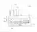
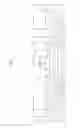
FIG. 1 show a prior art
FIG. 1 shows a prior art
FIG. 1 shows a chip package and a mother board 11. The chip package is ready to be mounted onto the mother board 11. The mother board 11 has a plurality of metal pads 113 on a bottom surface. The chip package has a plurality of solder balls 123 adaptive for electrically coupled to the metal pads 113 of the mother board 11. The chip package comprises a package substrate 12. The package substrate 12 has a plurality of top metal pads 121. A passivation layer 122 is configured on a top surface of the package substrate 12. A chip 13 is configured on a bottom of the package substrate 12. A finer metal connector to replace the solder ball connector is needed to develop for a compact chip package.
BRIEF DESCRIPTION OF THE DRAWINGS
FIG. 1 show a prior art.
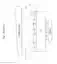
FIGS. 2A˜2C show an embodiment according to the present invention.
FIGS. 3˜2C show a fabricating process for the embodiment according to the present invention.
DETAILED DESCRIPTION OF THE INVENTION
A coaxial copper pillar is fabricated for maintaining a signal integrity during signal transmission. The coaxial copper pillar has a core copper pillar made for signal transmission and a dielectric layer wraps around the core copper pillar. A copper layer wraps around the dielectric layer as a signal shield.
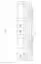
FIGS. 2A˜2C show an embodiment system according to the present invention.
FIG. 2A shows a mother board 21 having a coaxial metal pad 210 formed on a bottom surface of the mother board 121. The coaxial metal pad 210 comprises a core metal pad 211 and a circular metal pad 212. The circular metal pad 212 encircles the core metal pad 211. The core metal pad 211 is made electrically coupled to a signal line of an electronic system (not shown). The circular metal pad 212 is made electrically coupled to a ground line of the electronic system.
FIG. 2B shows a bottom view of the coaxial metal pad of FIG. 2A. FIG. 2B shows the circular metal pad 212 encircles the core metal pad 211. The circular metal pad 212 functions as a signal shield for the core metal pad 211.
FIG. 2C shows a chip package having a coaxial copper pillar according to the present invention.
FIG. 2C shows a package substrate 22. The package substrate 22 has a plurality of top metal pads 121. A coaxial copper pillar 310 is formed on a top surface of a selected top copper pillar 121.
The coaxial copper pillar 310 comprises a core copper pillar 125. The core copper pillar 125 has a bottom end electrically coupled to the selected top metal pad 121. The coaxial copper pillar 310 comprises a dielectric layer 225 wraps around an outer surface of the core copper pillar 125. Further, a copper layer 325 wraps around an outer surface of the dielectric layer 225.
The package substrate 22 comprises a first redistribution layer RDL1 and a second redistribution layer RDL2. The first redistribution layer RDL1 has a first redistribution circuitry RDC1 embedded in a first dielectric layer(s) D1, D2. The second redistribution layer RDL2 configured on a top surface of the first redistribution layer RDL1. The second redistribution layer RDL2 comprises a second redistribution circuitry RDC2 embedded in a second dielectric layer(s) D3, D4. The top metal pad 121 is configured on a top surface of the package substrate 22 and is a portion of the second redistribution circuit RDC2.
At lease one chip 13 is configured on a bottom surface of the package substrate 22. The chip 13 is electrically coupled to a bottom metal pad of the package substrate 22. An underfill material 126 is filled into a gap between the chip 13 and a bottom surface of the package substrate 22. A molding compound 127 encapsulates the chip 13.
A passivation layer 122 is configured on a top surface of the package substrate 22 and exposes a central area of the top metal pad 121 for further electrical connection.
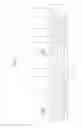
FIGS. 3˜21 show a fabricating process for a coaxial copper pillar according to the present invention.
A fabricating process for a coaxial copper pillar, comprises:
FIG. 3 shows: preparing a substrate 22; wherein at least one metal pad 121 is configured on a top surface of the substrate 22; a passivation 122 is configured on a top surface of the substrate 22; and a central area of the metal pad 121 is exposed;
FIG. 4 shows: forming a seed layer 123 on a top surface of each metal pad 121 and the passivation layer 122;
FIG. 5 shows: forming a first photoresist layer (PR1) on a top surface of the seed layer 123;
FIG. 6 shows: patterning the first photoresist layer (PR1) to form a plurality of first grooves 124;
FIG. 7 shows: plating to fill metal, e.g. copper, in each first groove 124 to form a plurality of copper pillars 125;
FIG. 8 shows: stripping the first photoresist layer (PR1);
FIG. 9 shows: stripping the seed layer 123 between the copper pillars 125;
FIG. 10 shows: forming a second photoresist layer (PR2) on a top surface of the passivation layer 122 and the copper pillars 125;
FIG. 11 shows: patterning the second photoresist layer (PR2) to form a plurality of second grooves 224 to expose selected copper pillars 125;
FIG. 12 shows: filling dielectric material 225 into the second grooves 224;
FIG. 13 shows: removing excessive materials on a top surface of the copper pillars 125;
FIG. 14 shows: stripping the second photoresist layer (PR2);
FIG. 15 shows: forming a third photoresist layer (PR3);
FIG. 16 shows: patterning the third photoresist layer (PR3) to form a plurality of third grooves 324 to expose the selected copper pillar 125 wrapped by the dielectric layer 225;
FIG. 17 shows: electroless plating to form copper layer 325, 325T wrapping an exposed surface of the dielectric layer; wherein the copper layer 325 wraps a side wall surface, and the copper layer 325T is configured on a top surface of the selected copper pillar 125 wrapped by the dielectric layer 225;
FIG. 18 shows: stripping the third photoresist layer (PR3);
FIG. 19 shows: removing the top copper layer 325T on a top surface of the copper pillar 125 wrapped by the dielectric layer 225;
FIG. 20 shows: mounting at least a chip 13 on a bottom surface of the bottom pads 221; and underfilling a space between the chip 13 and the substrate 22; and
FIG. 21 shows: singulating to form a plurality of chip package units.
While several embodiments have been described by way of example, it will be apparent to those skilled in the art that various modifications may be configured without departs from the spirit of the present invention. Such modifications are all within the scope of the present invention, as defined by the appended claims.
Claims
What is claimed is:1. A coaxial copper pillar, comprises:
a core copper pillar, configured on a top surface of a metal pad;
a dielectric layer, wrapping around an outer surface of the core copper pillar; and
a metal layer, wrapping around an outer surface of the dielectric layer.
2. A coaxial copper pillar as claimed in claim 1, further comprises:
a passivation layer, configured on a top surface of the metal pad and a central area of the metal pad is exposed; the metal pad is connected to a bottom end of the core copper pillar.
3. A coaxial copper pillar as claimed in claim 1, wherein the metal pad is a terminal pad of a circuitry, and the circuitry is embedded in a dielectric layer.
4. A coaxial copper pillar as claimed in claim 3, wherein the circuitry further comprises:
a bottom first redistribution circuitry, configured on a bottom end of the core copper pillars; the bottom first redistribution circuit is embedded in a first dielectric layer; and
a bottom second redistribution circuitry, configured on a bottom surface of the bottom first redistribution circuitry; the second redistribution circuitry is embedded in a second dielectric layer.
5. A circuit board having a coaxial metal pad, comprising:
a core metal pad, configured on a surface of the circuit board; and
a circular metal pad, encircling the core metal pad.
6. A fabricating process for a coaxial copper pillar, comprises:
preparing a substrate having a plurality of bottom pads and a plurality of top pads; a passivation, configured on a top surface of the substrate and a central area of the metal pad is exposed;
forming a seed layer on a top surface of each metal pad and the passivation layer;
forming a first photoresist layer (PR1) on a top surface of the seed layer;
patterning the first photoresist layer (PR1) to form a plurality of first grooves;
plating to fill metal in the grooves to form a plurality of copper pillars;
stripping the first photoresist layer (PR1);
stripping the seed layer between the copper pillars;
forming a second photoresist layer (PR2) on a top surface of the passivation layer and the copper pillars;
patterning the second photoresist layer (PR2) to form a plurality of second grooves to expose selected copper pillars;
filling dielectric material into the second grooves;
removing excessive materials on a top surface of the copper pillars;
stripping the second photoresist layer (PR2);
forming a third photoresist layer (PR3);
patterning the third photoresist layer (PR3) to form a plurality of third grooves to expose the selected copper pillar wrapped by the dielectric layer;
electroless plating to form copper layer wrapping an exposed surface of the dielectric layer;
stripping the third photoresist layer (PR3); and
removing the copper layer on a top surface of the copper pillar and the dielectric layer.
7. A fabricating process for a coaxial copper pillar as claimed in claim 6, comprises:
mounting at least a chip on a bottom surface of the bottom pads;
underfilling a space between the chip and the substrate; and
singulating to form a plurality of chip package units.
Images & Drawings included:


Sources:
- United States Patent and Trademark Office - verify current appl. status at the USPTO↗
Recent applications in this class:
- » 20250226305 2025-07-10
CIRCUIT BOARD AND SEMICONDUCTOR PACKAGE COMPRISING SAME - » 20250218925 2025-07-03
ELECTROLESS NICKEL-ELECTROLESS PALLADIUM-IMMERSION GOLD (ENEPIG) WITH THIN NICKEL LAYER AS A SURFACE FINISH FOR EMBEDDED DIE ATTACHMENTS - » 20250218924 2025-07-03
ELECTROLESS NICKEL-ELECTROLESS PALLADIUM-IMMERSION GOLD (ENEPIG) AS A SURFACE FINISH FOR EMBEDDED DIE ATTACHMENTS - » 20250174545 2025-05-29
ELECTRONIC DEVICES AND METHODS OF MANUFACTURING ELECTRONIC DEVICES - » 20250157913 2025-05-15
SEMICONDUCTOR DEVICE - » 20250014983 2025-01-09
ELECTRICALLY CONDUCTIVE VIAS AND METHODS FOR PRODUCING SAME - » 20240312900 2024-09-19
CHIP PACKAGE STRUCTURE WITH METAL-CONTAINING LAYER - » 20240304539 2024-09-12
METAL-CERAMIC MIXED PACKAGE SUBSTRATE PLATED WITH NON-MAGNETIC LAYER STACK - » 20240178126 2024-05-30
DOUBLE-SIDE COOLED POWER MODULES - » 20240153863 2024-05-09
SEMICONDUCTOR PACKAGE AND MANUFACTURING METHOD THEREOF