Manufacture method of AMOLED back plate and structure thereof
US20170077203A1
2017-03-16
15/340,948
2016-11-01
✅ Patent granted
US 9,947,736 B2
2018-04-17
-
-
Cheung Lee | Stephen C Smith
Andrew C. Cheng
2036-11-01
Abstract:
An AMOLED back plate includes a substrate on which a buffer layer and a poly-silicon section are sequentially formed. A source and a drain are respectively formed of P-type heavy doped micro silicon on the poly-silicon section that have edges facing and spaced from each other to define a channel therebetween. A gate isolation layer is formed on the buffer layer, the source, the drain and the channel. A gate is formed on the gate isolation layer and has opposite edges that face in directions toward the edges of the source and the drain. The opposite edges of the gate are spaced from the edges of the source and the drain by predetermined spacing distance in horizontal directions so as to prevent the gate from overlapping the source and the drain.
Assignee:
- Shenzhen China Star Optoelectronics Technology Co Ltd. 3,202 🇨🇳 Shenzhen, Guangdong, China
- SHENZHEN CHINA STAR OPTOELECTRONICS TECHNOLOGY CO., LTD. 1,397 🇨🇳 Shenzhen, China
Applicant:
Interested in similar patents?
Get notified when new applications in this technology area are published.
Classification:
H01L27/3262 » CPC main
Devices consisting of a plurality of semiconductor or other solid-state components formed in or on a common substrate including components using organic materials as the active part, or using a combination of organic materials with other materials as the active part with components specially adapted for light emission, e.g. flat-panel displays using organic light-emitting diodes [OLED]; Matrix-type displays; Active matrix displays special geometry or disposition of pixel-elements of TFT
H01L27/3246 » CPC further
Devices consisting of a plurality of semiconductor or other solid-state components formed in or on a common substrate including components using organic materials as the active part, or using a combination of organic materials with other materials as the active part with components specially adapted for light emission, e.g. flat-panel displays using organic light-emitting diodes [OLED]; Matrix-type displays; Active matrix displays Pixel defining structures, e.g. banks
H01L27/3248 » CPC further
Devices consisting of a plurality of semiconductor or other solid-state components formed in or on a common substrate including components using organic materials as the active part, or using a combination of organic materials with other materials as the active part with components specially adapted for light emission, e.g. flat-panel displays using organic light-emitting diodes [OLED]; Matrix-type displays; Active matrix displays Connection of the pixel electrode to the TFT
H01L27/3265 » CPC further
Devices consisting of a plurality of semiconductor or other solid-state components formed in or on a common substrate including components using organic materials as the active part, or using a combination of organic materials with other materials as the active part with components specially adapted for light emission, e.g. flat-panel displays using organic light-emitting diodes [OLED]; Matrix-type displays; Active matrix displays special geometry or disposition of pixel-elements of capacitor
H01L51/5215 » CPC further
Solid state devices using organic materials as the active part, or using a combination of organic materials with other materials as the active part; Processes or apparatus specially adapted for the manufacture or treatment of such devices, or of parts thereof specially adapted for light emission, e.g. organic light emitting diodes [OLED] or polymer light emitting devices [PLED]; Details of devices; Electrodes; Anodes, i.e. with high work-function material composed of transparent multilayers
H01L27/32 IPC
Devices consisting of a plurality of semiconductor or other solid-state components formed in or on a common substrate including components using organic materials as the active part, or using a combination of organic materials with other materials as the active part with components specially adapted for light emission, e.g. flat-panel displays using organic light-emitting diodes [OLED]
H01L51/52 IPC
Solid state devices using organic materials as the active part, or using a combination of organic materials with other materials as the active part; Processes or apparatus specially adapted for the manufacture or treatment of such devices, or of parts thereof specially adapted for light emission, e.g. organic light emitting diodes [OLED] or polymer light emitting devices [PLED] Details of devices
H01L21/0262 » CPC further
Processes or apparatus adapted for the manufacture or treatment of semiconductor or solid state devices or of parts thereof; Manufacture or treatment of semiconductor devices or of parts thereof; Forming layers; Forming inorganic semiconducting materials on a substrate; Formation types; Deposition types Reduction or decomposition of gaseous compounds, e.g. CVD
H01L27/1255 » CPC further
Devices consisting of a plurality of semiconductor or other solid-state components formed in or on a common substrate including semiconductor components specially adapted for rectifying, oscillating, amplifying or switching and having at least one potential-jump barrier or surface barrier; including integrated passive circuit elements with at least one potential-jump barrier or surface barrier the substrate being other than a semiconductor body, e.g. an insulating body comprising a plurality of TFTs formed on a non-semiconducting substrate, e.g. driving circuits for AMLCDs integrated with passive devices, e.g. auxiliary capacitors
H01L29/41775 » CPC further
Semiconductor devices adapted for rectifying, amplifying, oscillating or switching, or capacitors or resistors with at least one potential-jump barrier or surface barrier, e.g. PN junction depletion layer or carrier concentration layer; Details of semiconductor bodies or of electrodes thereof; Multistep manufacturing processes therefor; Electrodes ; Multistep manufacturing processes therefor characterised by their shape, relative sizes or dispositions carrying the current to be rectified, amplified or switched; Source or drain electrodes for field effect devices characterised by the proximity or the relative position of the source or drain electrode and the gate electrode, e.g. the source or drain electrode separated from the gate electrode by side-walls or spreading around or above the gate electrode
H01L29/458 » CPC further
Semiconductor devices adapted for rectifying, amplifying, oscillating or switching, or capacitors or resistors with at least one potential-jump barrier or surface barrier, e.g. PN junction depletion layer or carrier concentration layer; Details of semiconductor bodies or of electrodes thereof; Multistep manufacturing processes therefor; Electrodes ; Multistep manufacturing processes therefor characterised by the materials of which they are formed; Ohmic electrodes on silicon for thin film silicon, e.g. source or drain electrode
H01L29/4908 » CPC further
Semiconductor devices adapted for rectifying, amplifying, oscillating or switching, or capacitors or resistors with at least one potential-jump barrier or surface barrier, e.g. PN junction depletion layer or carrier concentration layer; Details of semiconductor bodies or of electrodes thereof; Multistep manufacturing processes therefor; Electrodes ; Multistep manufacturing processes therefor characterised by the materials of which they are formed; Metal-insulator-semiconductor electrodes, e.g. gates of MOSFET for thin film semiconductor, e.g. gate of TFT
H01L29/4958 » CPC further
Semiconductor devices adapted for rectifying, amplifying, oscillating or switching, or capacitors or resistors with at least one potential-jump barrier or surface barrier, e.g. PN junction depletion layer or carrier concentration layer; Details of semiconductor bodies or of electrodes thereof; Multistep manufacturing processes therefor; Electrodes ; Multistep manufacturing processes therefor characterised by the materials of which they are formed; Metal-insulator-semiconductor electrodes, e.g. gates of MOSFET the conductor material next to the insulator being a simple metal, e.g. W, Mo with a multiple layer structure
H01L51/56 » CPC further
Solid state devices using organic materials as the active part, or using a combination of organic materials with other materials as the active part; Processes or apparatus specially adapted for the manufacture or treatment of such devices, or of parts thereof specially adapted for light emission, e.g. organic light emitting diodes [OLED] or polymer light emitting devices [PLED] Processes or apparatus specially adapted for the manufacture or treatment of such devices or of parts thereof
H01L27/1222 » CPC further
Devices consisting of a plurality of semiconductor or other solid-state components formed in or on a common substrate including semiconductor components specially adapted for rectifying, oscillating, amplifying or switching and having at least one potential-jump barrier or surface barrier; including integrated passive circuit elements with at least one potential-jump barrier or surface barrier the substrate being other than a semiconductor body, e.g. an insulating body comprising a plurality of TFTs formed on a non-semiconducting substrate, e.g. driving circuits for AMLCDs with a particular composition, shape or crystalline structure of the active layer
H01L27/1274 » CPC further
Devices consisting of a plurality of semiconductor or other solid-state components formed in or on a common substrate including semiconductor components specially adapted for rectifying, oscillating, amplifying or switching and having at least one potential-jump barrier or surface barrier; including integrated passive circuit elements with at least one potential-jump barrier or surface barrier the substrate being other than a semiconductor body, e.g. an insulating body comprising a plurality of TFTs formed on a non-semiconducting substrate, e.g. driving circuits for AMLCDs; Multistep manufacturing methods with a particular formation, treatment or patterning of the active layer specially adapted to the circuit arrangement using crystallisation of amorphous semiconductor or recrystallisation of crystalline semiconductor
H01L29/7833 » CPC further
Semiconductor devices adapted for rectifying, amplifying, oscillating or switching, or capacitors or resistors with at least one potential-jump barrier or surface barrier, e.g. PN junction depletion layer or carrier concentration layer; Details of semiconductor bodies or of electrodes thereof; Multistep manufacturing processes therefor; Types of semiconductor device ; Multistep manufacturing processes therefor controllable by only the electric current supplied, or only the electric potential applied, to an electrode which does not carry the current to be rectified, amplified or switched; Unipolar devices, e.g. field effect transistors; Field effect transistors with field effect produced by an insulated gate with lightly doped drain or source extension, e.g. LDD MOSFET's; DDD MOSFET's
H01L2227/323 » CPC further
Indexing scheme for devices consisting of a plurality of semiconductor or other solid state components formed in or on a common substrate covered by group; Devices including an organic light emitting device [OLED], e.g. OLED display Multistep processes for AMOLED
H01L2251/301 » CPC further
Indexing scheme relating to organic semiconductor devices covered by group; Materials Inorganic materials
H01L2251/306 » CPC further
Indexing scheme relating to organic semiconductor devices covered by group; Materials; Inorganic materials; Oxides, e.g. metal oxides; Transparent conductive oxides [TCO] composed of tin oxides, e.g. F doped SnO
H01L2251/308 » CPC further
Indexing scheme relating to organic semiconductor devices covered by group; Materials; Inorganic materials; Oxides, e.g. metal oxides; Transparent conductive oxides [TCO] composed of indium oxides, e.g. ITO
H01L29/45 IPC
Semiconductor devices adapted for rectifying, amplifying, oscillating or switching, or capacitors or resistors with at least one potential-jump barrier or surface barrier, e.g. PN junction depletion layer or carrier concentration layer; Details of semiconductor bodies or of electrodes thereof; Multistep manufacturing processes therefor; Electrodes ; Multistep manufacturing processes therefor characterised by the materials of which they are formed Ohmic electrodes
H01L27/12 IPC
Devices consisting of a plurality of semiconductor or other solid-state components formed in or on a common substrate including semiconductor components specially adapted for rectifying, oscillating, amplifying or switching and having at least one potential-jump barrier or surface barrier; including integrated passive circuit elements with at least one potential-jump barrier or surface barrier the substrate being other than a semiconductor body, e.g. an insulating body
H01L29/49 IPC
Semiconductor devices adapted for rectifying, amplifying, oscillating or switching, or capacitors or resistors with at least one potential-jump barrier or surface barrier, e.g. PN junction depletion layer or carrier concentration layer; Details of semiconductor bodies or of electrodes thereof; Multistep manufacturing processes therefor; Electrodes ; Multistep manufacturing processes therefor characterised by the materials of which they are formed Metal-insulator-semiconductor electrodes, e.g. gates of MOSFET
H01L21/02 IPC
Processes or apparatus adapted for the manufacture or treatment of semiconductor or solid state devices or of parts thereof Manufacture or treatment of semiconductor devices or of parts thereof
H01L29/786 IPC
Semiconductor devices adapted for rectifying, amplifying, oscillating or switching, or capacitors or resistors with at least one potential-jump barrier or surface barrier, e.g. PN junction depletion layer or carrier concentration layer; Details of semiconductor bodies or of electrodes thereof; Multistep manufacturing processes therefor; Types of semiconductor device ; Multistep manufacturing processes therefor controllable by only the electric current supplied, or only the electric potential applied, to an electrode which does not carry the current to be rectified, amplified or switched; Unipolar devices, e.g. field effect transistors; Field effect transistors with field effect produced by an insulated gate Thin film transistors, i.e. transistors with a channel being at least partly a thin film
H01L21/306 IPC
Processes or apparatus adapted for the manufacture or treatment of semiconductor or solid state devices or of parts thereof; Manufacture or treatment of semiconductor devices or of parts thereof the devices having at least one potential-jump barrier or surface barrier, e.g. PN junction, depletion layer or carrier concentration layer the devices having semiconductor bodies comprising elements of Group IV of the Periodic System or AB compounds with or without impurities, e.g. doping materials; Treatment of semiconductor bodies using processes or apparatus not provided for in groups - to change their surface-physical characteristics or shape, e.g. etching, polishing, cutting Chemical or electrical treatment, e.g. electrolytic etching
H01L29/66 IPC
Semiconductor devices adapted for rectifying, amplifying, oscillating or switching, or capacitors or resistors with at least one potential-jump barrier or surface barrier, e.g. PN junction depletion layer or carrier concentration layer; Details of semiconductor bodies or of electrodes thereof; Multistep manufacturing processes therefor Types of semiconductor device ; Multistep manufacturing processes therefor
H01L29/417 IPC
Semiconductor devices adapted for rectifying, amplifying, oscillating or switching, or capacitors or resistors with at least one potential-jump barrier or surface barrier, e.g. PN junction depletion layer or carrier concentration layer; Details of semiconductor bodies or of electrodes thereof; Multistep manufacturing processes therefor; Electrodes ; Multistep manufacturing processes therefor characterised by their shape, relative sizes or dispositions carrying the current to be rectified, amplified or switched
H01L29/78 IPC
Semiconductor devices adapted for rectifying, amplifying, oscillating or switching, or capacitors or resistors with at least one potential-jump barrier or surface barrier, e.g. PN junction depletion layer or carrier concentration layer; Details of semiconductor bodies or of electrodes thereof; Multistep manufacturing processes therefor; Types of semiconductor device ; Multistep manufacturing processes therefor controllable by only the electric current supplied, or only the electric potential applied, to an electrode which does not carry the current to be rectified, amplified or switched; Unipolar devices, e.g. field effect transistors; Field effect transistors with field effect produced by an insulated gate
Description
CROSS REFERENCE TO RELATED APPLICATIONS
This is a divisional application of co-pending U.S. patent application Ser. No. 14/429,082, filed on Mar. 18, 2015.
BACKGROUND OF THE INVENTION
1. Field of the Invention
The present invention relates to a display technology field, and more particularly to a manufacture method of an AMOLED back plate and a structure thereof.
2. The Related Arts
In the display field, liquid crystal display (LCD), organic light emitting diode (OLED) and other panel display techniques have been gradually replaced the conventional cathode ray tube (CRT) displays. The OLED possesses many outstanding properties of self-illumination, low driving voltage, high luminescence efficiency, fast response, high clarity and contrast, near 180° view angle, wide range of working temperature, applicability of flexible display and large scale full color display. The OLED is considered as the most potential flat panel display technology.
The OLED can be categorized as passive matrix OLED (PMOLED) and active matrix OLED (AMOLED) according to the driving types. Generally, the AMOLED comprises a low temperature poly-silicon (LTPS) drive back plate and an electroluminescence layer for being the self-illumination component. The low temperature poly-silicon possesses higher electron mobility. For the AMOLED, the LTPS material possesses advantages of high resolution, fast response, high brightness, high aperture ratio, low power consumption, et cetera.
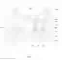
A structure of an AMOLED back plate according to prior art is shown in FIG. 1. The manufacture process of the AMOLED back plate generally is:
step 1, deposing a buffer layer 200 on a glass substrate 100;
step 2, deposing an amorphous silicon layer (a-Si) on the buffer layer 200, and using the Laser process to make the amorphous silicon layer to be crystallized and converted to be a poly-silicon layer (Poly-Si);
step 3, patterning the poly-silicon layer with photo and etch processes to form a first poly-silicon section 301 and a second poly-silicon section 303;
step 4, deposing an N type heavy doped amorphous silicon layer N+a-Si on the buffer layer 200, the first poly-silicon section 301 and the second poly-silicon section 303, and implementing the photo process to define the position of a channel 400, and etching to pattern the N type heavy doped amorphous silicon layer N+a-Si for forming a source/a drain 401 on the first poly-silicon section 301 and an electrode 403 on the second poly-silicon section 303 except an area corresponding to the channel 400;
step 5, deposing and patterning the gate isolation layer 500 on the buffer layer 200, the source/the drain 401 and the electrode 403;
step 6, deposing and patterning a first metal layer on the gate isolation layer 500 to form a gate 601 and a metal electrode 603, wherein the gate 601 is above the source/the drain 401 and partially overlaps the source/the drain 401 in a horizontal direction;
step 7, sequentially forming an interlayer insulation layer 700, a metal source/a metal drain 801, a flat layer 900, an anode 1000, a pixel definition layer 1100 and a photo spacer 1200 on the gate isolation layer 500, the gate 601 and the metal electrode 603 with deposition, photo and etch processes.
The metal source/the metal drain 801 are electrically connected to the source/the drain 401; and the anode 1000 is electrically connected to the metal source/the metal drain 801.
The first poly-silicon section 301, the source/the drain 401, the gate 601 and the metal source/the metal drain 801 construct a drive TFT, and the second poly-silicon section 303, the electrode 403 and the metal electrode 603 construct a storage capacitor.
The drive TFT of the AMOLED back plate shown in FIG. 1 is an NMOS, and the AMOLED panel may suffer image sticking more easily. Besides, the contact resistance between the source/the drain 401 formed with the N type heavy doped amorphous silicon layer N+a-Si and the first poly-silicon section 301 is higher, and thus, the conductive current of the drive TFT can be lower. In addition, the source/the drain 401 and the gate 601 partially overlap each other in the horizontal direction and this may cause a leakage current of the drive TFT to be excessively high.
SUMMARY OF THE INVENTION
An objective of the present invention is to provide a manufacture method of an AMOLED back plate, which can improve the electrical property of a drive TFT to make a conductive current higher and a leakage current lower, and diminish image sticking for raising the display quality of the AMOLED.
Another objective of the present invention is to provide an AMOLED back plate, which can improve the electrical property of the drive TFT to make a conductive current higher and a leakage current lower, and diminish image sticking for raising the display quality of the AMOLED.
For realizing the aforesaid objectives, the present invention provides a manufacture method of an AMOLED back plate, which comprises sequentially deposing a buffer layer, an amorphous silicon layer on a substrate, and crystallizing and converting the amorphous silicon layer to be a poly-silicon layer, and patterning the poly-silicon layer, and then deposing a P type heavy doped micro silicon layer, and implementing a photo process to define a position of a channel, and etching the P type heavy doped micro silicon layer to form a source/a drain, and thereafter, sequentially forming a gate isolation layer, a gate, an interlayer insulation layer, a metal source/a metal drain, a flat layer, an anode, a pixel definition layer and a photo spacer; the source/the drain and the gate do not overlap in the horizontal direction and are mutually spaced.
The manufacture method of the AMOLED back plate comprises the following steps:
step 1, providing a substrate and deposing a buffer layer on the substrate;
step 2, deposing an amorphous silicon layer on the buffer layer and implementing an excimer laser annealing process to the amorphous silicon layer to make the amorphous silicon layer crystallized and converted into a poly-silicon layer;
step 3, patterning the poly-silicon layer with photo and etch processes to form a first poly-silicon section and a second poly-silicon section;
step 4, deposing a P type heavy doped micro silicon layer on the buffer layer, the first poly-silicon section and the second poly-silicon section; implementing a photo process to define a position of a channel; and etching the P type heavy doped micro silicon layer to pattern the P type heavy doped micro silicon layer for forming a source/a drain on the first poly-silicon section and an electrode on the second poly-silicon section except an area corresponding to the channel;
step 5, deposing and patterning a gate isolation layer on the buffer layer, the source/the drain and the electrode;
step 6, deposing and patterning a first metal layer on the gate isolation layer to form a gate and a metal electrode;
wherein the gate is above the channel and the source/the drain and the gate are mutually spaced with a certain distance in a horizontal direction;
step 7, sequentially forming an interlayer insulation layer, a metal source/a metal drain, a flat layer, an anode, a pixel definition layer, and a photo spacer on the gate isolation layer, the gate and the metal electrode with deposition, photo and etch processes;
wherein the metal source/the metal drain are electrically connected to the source/the drain; and the anode is electrically connected to the metal source/the metal drain; and
wherein the first poly-silicon section, the source/the drain, the gate and the metal source/the metal drain construct a drive TFT, and the second poly-silicon section, the electrode and the metal electrode construct a storage capacitor.
In the step 4, the P type heavy doped micro silicon layer is deposed by chemical vapor deposition (CVD).
The mutually spaced distance of the source/the drain and the gate in the horizontal direction is 0.1-0.5 μm.
A material of the gate is a stacked combination of one or more of molybdenum, titanium, aluminum and copper.
A material of the buffer layer is silicon nitride, silicon oxide, or a combination thereof; and a material of the interlayer insulation layer is silicon oxide, silicon nitride or a combination thereof.
A material of the anode is an indium tin oxide/silver/indium tin oxide compound thin film.
The present invention further provides a structure of an AMOLED back plate, comprising a substrate, a buffer layer located on the substrate, a first poly-silicon section and a second poly-silicon section arranged in space on the buffer layer, a source/a drain and an electrode respectively located on the first poly-silicon section and the second poly-silicon section, a gate isolation layer located on the buffer layer, the source/the drain and the electrode, a gate and a metal electrode located on the gate isolation layer, and an interlayer insulation layer, a metal source/a metal drain, a flat layer, an anode, a pixel definition layer and a photo spacer, sequentially formed on the gate isolation layer, the gate and the metal electrode, wherein the metal source/the metal drain are electrically connected to the source/the drain and the anode is electrically connected to the metal source/the metal drain;
wherein a material of the source/the drain is P type heavy doped micro silicon; a channel is located between the source/the drain; and the gate is above the channel and the source/the drain and the gate are mutually spaced in a horizontal direction;
wherein the first poly-silicon section, the source/the drain, the gate and the metal source/the metal drain construct a drive TFT, and the second poly-silicon section, the electrode and the metal electrode construct a storage capacitor.
The mutually spaced distance of the source/the drain and the gate in the horizontal direction is 0.1-0.5 μm.
A material of the gate is a stacked combination of one or more of molybdenum, titanium, aluminum and copper; a material of the buffer layer is silicon nitride, silicon oxide, or a combination thereof; a material of the interlayer insulation layer is silicon oxide, silicon nitride or a combination thereof; and a material of the anode is an indium tin oxide/silver/indium tin oxide compound thin film.
The present invention further provides a structure of an AMOLED back plate, comprising a substrate, a buffer layer located on the substrate, a first poly-silicon section and a second poly-silicon section arranged in space on the buffer layer, a source/a drain and an electrode respectively located on the first poly-silicon section and the second poly-silicon section, a gate isolation layer located on the buffer layer, the source/the drain and the electrode, a gate and a metal electrode located on the gate isolation layer, and an interlayer insulation layer, a metal source/a metal drain, a flat layer, an anode, a pixel definition layer and a photo spacer, sequentially formed on the gate isolation layer, the gate and the metal electrode, wherein the metal source/the metal drain are electrically connected to the source/the drain and the anode is electrically connected to the metal source/the metal drain;
wherein a material of the source/the drain is P type heavy doped micro silicon; a channel is located between the source/the drain; the gate is above the channel, and the source/the drain and the gate are mutually spaced in a horizontal direction;
wherein the first poly-silicon section, the source/the drain, the gate and the metal source/the metal drain construct a drive TFT, and the second poly-silicon section, the electrode and the metal electrode construct a storage capacitor;
wherein the mutually spaced distance of the source/the drain and the gate in the horizontal direction is 0.1-0.5 μm;
wherein a material of the gate is a stacked combination of one or more of molybdenum, titanium, aluminum and copper; a material of the buffer layer is silicon nitride, silicon oxide, or a combination thereof; a material of the interlayer insulation layer is silicon oxide, silicon nitride or a combination thereof; and a material of the anode is an indium tin oxide/silver/indium tin oxide compound thin film.
The benefits of the present invention are as follows. The present invention provides a manufacture method of an AMOLED back plate, in which by deposing and patterning a P type heavy doped micro silicon layer to form a source/a drain, and making the source/the drain and a gate be mutually spaced in a horizontal direction, the contact resistance between the source/the drain and a first poly-silicon section can be reduced to improve the electrical property of a drive TFT to make a conductive current higher and a leakage current lower, and diminish image sticking for raising the display quality of the AMOLED. The present invention also provides a structure of an AMOLED back plate, in which by locating a source/a drain of which a material is P type heavy doped micro silicon such that the source/the drain and a gate are mutually spaced in a horizontal direction, the contact resistance between the source/the drain and a first poly-silicon section can be reduced to improve the electrical property of a drive TFT to make a conductive current higher and a leakage current lower, and diminish image sticking for raising the display quality of the AMOLED.
BRIEF DESCRIPTION OF THE DRAWINGS
The technical solution and the beneficial effects of the present invention are best understood from the following detailed description with reference to the accompanying figures and embodiments.
In the drawings:
FIG. 1 is a diagram of an AMOLED back plate structure according to prior art;
FIG. 2 is a flowchart of a manufacture method of an AMOLED back plate according to the present invention;
FIG. 3 is a diagram of step 3 in the manufacture method of the AMOLED back plate according to the present invention;
FIG. 4 is a diagram of step 4 in the manufacture method of the AMOLED back plate according to the present invention;
FIG. 5 is a diagram of step 5 in the manufacture method of the AMOLED back plate according to the present invention;
FIG. 6 is a diagram of step 6 in the manufacture method of the AMOLED back plate according to the present invention; and
FIG. 7 is a diagram of step 7 in the manufacture method of the AMOLED back plate and a diagram of a structure of the AMOLED back plate according to the present invention.
DETAILED DESCRIPTION OF THE PREFERRED EMBODIMENTS
For better explaining the technical solution and the effect of the present invention, the present invention will be further described in detail with the accompanying drawings and the specific embodiments.
Referring to FIGS. 2-7, the present invention provides a manufacture method of an AMOLED back plate, comprising the following steps:
step 1, providing a substrate 1 and deposing a buffer layer 2 on the substrate 1.
The substrate 1 is a transparent substrate. Preferably, the substrate 1 is a glass substrate or a plastic substrate.
A material of the buffer layer 2 is silicon nitride (SiNx), silicon oxide (SiOx), or a combination thereof.
step 2, deposing an amorphous silicon layer on the buffer layer 2, and implementing an excimer laser annealing process to the amorphous silicon layer to make the amorphous silicon layer crystallized and converted into a poly-silicon layer.
step 3, as shown in FIG. 3, patterning the poly-silicon layer with photo and etch processes to form a first poly-silicon section 31 and a second poly-silicon section 33.
step 4, as shown in FIG. 4, deposing a P type heavy doped micro silicon (P+micro-crystallized Si) layer P+uc-Si on the buffer layer 2, the first poly-silicon section 31 and the second poly-silicon section 33 by chemical vapor deposition (CVD); implementing a photo process to define a position of a channel 40; and etching the P type heavy doped micro silicon layer P+uc-Si to pattern the P type heavy doped micro silicon layer P+uc-Si for forming a source/a drain 41 on the first poly-silicon section 31 and an electrode 43 on the second poly-silicon section 33 except an area corresponding to the channel 40.
step 5, as shown in FIG. 5, deposing and patterning a gate isolation layer 5 on the buffer layer 2, the source/the drain 41 and the electrode 43.
step 6, as shown in FIG. 6, deposing and patterning a first metal layer on the gate isolation layer 5 to form a gate 61 and a metal electrode 63.
The gate 61 is located above the channel 40, and the source/the drain 41 and the gate 61 are mutually spaced with a certain distance in a horizontal direction. Furthermore, the mutually spaced distance of the source/the drain 41 and the gate 61 in the horizontal direction is 0.1-0.5 μm.
A material of the gate 61 and the metal electrode 63 is a stacked combination of one or more of molybdenum (Mo), titanium (Ti), aluminum (Al) and copper (Cu).
step 7, as shown in FIG. 7, sequentially forming an interlayer insulation layer 7, a metal source/a metal drain 81, a flat layer 9, an anode 10, a pixel definition layer 11, and a photo spacer 12 on the gate isolation layer 5, the gate 61 and the metal electrode 63 with deposition, photo and etch processes.
The metal source/the metal drain 81 are electrically connected to the source/the drain 41; and the anode 10 is electrically connected to the metal source/the metal drain 81.
A material of the interlayer insulation layer 7 is silicon oxide, silicon nitride or a combination thereof. A material of the anode 10 is an indium tin oxide/silver/indium tin oxide (ITO/Ag/ITO) compound thin film.
The first poly-silicon section 31, the source/the drain 41, the gate 61 and the metal source/the metal drain 81 construct a drive TFT, and the second poly-silicon section 33, the electrode 43 and the metal electrode 63 construct a storage capacitor.
In the aforesaid manufacture method of the AMOLED back plate, the source/the drain 41 is obtained by deposing and patterning a P type heavy doped micro silicon layer P+uc-Si, and thus, the drive TFT is a P type TFT, and the AMOLED driven by the P type TFT can diminish image sticking to thus improve the display quality of the AMOLED. Further, the material property of the P type heavy doped micro silicon is more similar with that of the poly-silicon, and thus, the contact resistance between the source/the drain 41 and the first poly-silicon section 31 can be reduced to improve the electrical property of the drive TFT to make a conductive current higher. The source/the drain 41 and the gate 61 are mutually spaced in the horizontal direction with no overlapping area therebetween so as to make a leakage current of the drive TFT lower.
Referring to FIG. 7, the present invention also provides a structure of an AMOLED back plate, which comprises a substrate 1, a buffer layer 2 located on the substrate 1, a first poly-silicon section 31 and a second poly-silicon section 33 arranged in space on the buffer layer 2, a source/a drain 41 and an electrode 43 respectively located on the first poly-silicon section 31 and the second poly-silicon section 33, a gate isolation layer 5 located on the buffer layer 2, the source/the drain 41 and the electrode 43, a gate 61 and a metal electrode 63 located on the gate isolation layer 5, and an interlayer insulation layer 7, a metal source/a metal drain 81, a flat layer 9, an anode 10, a pixel definition layer 11 and a photo spacer 12 sequentially formed on the gate isolation layer 5, the gate 61 and the metal electrode 63.
The metal source/the metal drain 81 are electrically connected to the source/the drain 41. The anode 10 is electrically connected to the metal source/the metal drain 81. The first poly-silicon section 31, the source/the drain 41, the gate 61 and the metal source/the metal drain 81 construct a drive TFT, and the second poly-silicon section 33, the electrode 43 and the metal electrode 63 construct a storage capacitor.
A material of the source/the drain 41 is P type heavy doped micro silicon (P+uc-Si). A channel 40 is located between the source/the drain 41. The gate 61 is located above the channel 40. The source/the drain 41 and the gate 61 do not overlap each other and are mutually spaced in a horizontal direction. Furthermore, the mutually spaced distance between the source/the drain 41 and the gate 61 in the horizontal direction is 0.1-0.5 μm.
Specifically, the substrate 1 is a transparent substrate. Preferably, the substrate 1 is a glass substrate or a plastic substrate. A material of the gate 61 is a stacked combination of one or more of molybdenum, titanium, aluminum and copper. A material of the buffer layer 2 is silicon nitride, silicon oxide, or a combination thereof. A material of the interlayer insulation layer 7 is silicon oxide, silicon nitride or a combination thereof. A material of the anode 10 is an indium tin oxide/silver/indium tin oxide compound thin film.
In the aforesaid structure of AMOLED back plate, the material of the source/the drain 41 is P type heavy doped micro silicon P+uc-Si, and thus, the drive TFT is a P type TFT, and the AMOLED driven by the P type TFT can diminish image sticking and thus improving the display quality of the AMOLED. Further, the material property of the P type heavy doped micro silicon is more similar with that of the poly-silicon, and thus, the contact resistance between the source/the drain 41 and the first poly-silicon section 31 can be reduced to improve the electrical property of the drive TFT to make a conductive current higher. The source/the drain 41 and the gate 61 are mutually spaced in the horizontal direction with no overlapping area therebetween so as to make a leakage current of the drive TFT lower.
In conclusion, in the manufacture method of an AMOLED back plate of the present invention, by deposing and patterning a P type heavy doped micro silicon layer to form a source/a drain and making the source/the drain and a gate be mutually spaced in a horizontal direction, the contact resistance between the source/the drain and a first poly-silicon section can be reduced to improve the electrical property of the drive TFT to make a conductive current higher and a leakage current lower, and diminish image sticking for raising the display quality of the AMOLED. In a structure of an AMOLED back plate of the present invention, by locating a source/a drain of which a material is P type heavy doped micro silicon such that the source/the drain and a gate are mutually spaced from each other in a horizontal direction, the contact resistance between the source/the drain and a first poly-silicon section can be reduced to improve the electrical property of the drive TFT to make a conductive current higher and a leakage current lower, and diminish image sticking for raising the display quality of the AMOLED.
The above provides only specific embodiments of the present invention, and the scope of the present invention is not limited to it. To those skilled in the art, modification or substitution that are easily derived should be covered by the protection scope sought for the invention. Thus, the scope of the invention should be defined by the appended claims.
Claims
What is claimed is:1. An active matrix organic light emitting diode (AMOLED) back plate, comprising:
a substrate;
a buffer layer located on the substrate;
a first poly-silicon section and a second poly-silicon section arranged on the buffer layer and spaced from each other;
a source/a drain and an electrode respectively located on the first poly-silicon section and the second poly-silicon section;
a gate isolation layer located on the buffer layer, the source/the drain and the electrode;
a gate and a metal electrode formed on the gate isolation layer; and
an interlayer insulation layer, a metal source/a metal drain, a flat layer, an anode, a pixel definition layer, and a photo spacer, which are sequentially formed on the gate isolation layer, the gate and the metal electrode such that the metal source/the metal drain are electrically connected to the source/the drain and the anode is electrically connected to the metal source/the metal drain;
wherein the source/the drain is formed of a material comprising P type heavy doped micro silicon, such that a first portion of the P type heavy doped micro silicon that forms the source and a second portion of the P type heavy doped micro silicon that forms drain respectively have a first edge and a second edge, which face each other and are spaced from each other by a spacing distance in which a channel is formed and located between the source and the drain; and the gate that is formed on the gate isolation layer is located above the channel such that the gate has opposite side edges respectively facing in directions toward the first edge of the first portion of the P type heavy doped micro silicon and the second edge of the second portion of the P type heavy doped micro silicon and the opposite side edges of the gate are respectively spaced, in horizontal directions, from the first and second edges of the first and second portions of the P type heavy doped micro silicon by predetermined spacing distances to prevent the gate from overlapping the source and the drain; and
wherein the first poly-silicon section, the source/the drain, the gate, and the metal source/the metal drain construct a drive TFT, and the second poly-silicon section, the electrode, and the metal electrode construct a storage capacitor.
2. The AMOLED back plate as claimed in claim 1, wherein the predetermined spacing distances between the opposite edges of the gate and the first and second edges of the first and second portions of the P type heavy doped micro silicon are each within a range of 0.1-0.5 μm.
3. The AMOLED back plate as claimed in claim 1, wherein the gate is formed of a material that comprises a stacked combination of one or more of molybdenum, titanium, aluminum and copper.
4. The AMOLED back plate as claimed in claim 1, wherein the buffer layer is formed of a material comprising one of silicon nitride and silicon oxide, or a combination thereof.
5. The AMOLED back plate as claimed in claim 1, wherein the interlayer insulation layer is formed of a material comprising one of silicon oxide and silicon nitride or a combination thereof.
6. The AMOLED back plate as claimed in claim 1, wherein the anode comprises an indium tin oxide/silver/indium tin oxide compound film.
7. An active matrix organic light emitting diode (AMOLED) back plate, comprising:
a substrate;
a buffer layer located on the substrate;
a first poly-silicon section and a second poly-silicon section arranged on the buffer layer and spaced from each other;
a source/a drain and an electrode respectively located on the first poly-silicon section and the second poly-silicon section;
a gate isolation layer located on the buffer layer, the source/the drain and the electrode;
a gate and a metal electrode formed on the gate isolation layer; and
an interlayer insulation layer, a metal source/a metal drain, a flat layer, an anode, a pixel definition layer, and a photo spacer, which are sequentially formed on the gate isolation layer, the gate and the metal electrode such that the metal source/the metal drain are electrically connected to the source/the drain and the anode is electrically connected to the metal source/the metal drain;
wherein the source/the drain is formed of a material comprising P type heavy doped micro silicon, such that a first portion of the P type heavy doped micro silicon that forms the source and a second portion of the P type heavy doped micro silicon that forms drain respectively have a first edge and a second edge, which face each other and are spaced from each other by a spacing distance in which a channel is formed and located between the source and the drain; and the gate that is formed on the gate isolation layer is located above the channel such that the gate has opposite side edges respectively facing in directions toward the first edge of the first portion of the P type heavy doped micro silicon and the second edge of the second portion of the P type heavy doped micro silicon and the opposite side edges of the gate are respectively spaced, in horizontal directions, from the first and second edges of the first and second portions of the P type heavy doped micro silicon by predetermined spacing distances to prevent the gate from overlapping the source and the drain;
wherein the first poly-silicon section, the source/the drain, the gate, and the metal source/the metal drain construct a drive TFT, and the second poly-silicon section, the electrode, and the metal electrode construct a storage capacitor;
and wherein the predetermined spacing distances between the opposite edges of the gate and the first and second edges of the first and second portions of the P type heavy doped micro silicon are each within a range of 0.1-0.5 μm.
8. The AMOLED back plate as claimed in claim 7, wherein the gate is formed of a material that comprises a stacked combination of one or more of molybdenum, titanium, aluminum and copper.
9. The AMOLED back plate as claimed in claim 7, wherein the buffer layer is formed of a material comprising one of silicon nitride and silicon oxide, or a combination thereof.
10. The AMOLED back plate as claimed in claim 7, wherein the interlayer insulation layer is formed of a material comprising one of silicon oxide and silicon nitride or a combination thereof.
11. The AMOLED back plate as claimed in claim 7, wherein the anode comprises an indium tin oxide/silver/indium tin oxide compound film.
Images & Drawings included:


Sources:
- United States Patent and Trademark Office - verify current appl. status at the USPTO↗
Similar patent applications:
Recent applications in this class:
- » 20240237401 2024-07-11
DISPLAY PANEL, METHOD OF FABRICATING SAME AND DISPLAY DEVICE - » 20240237400 2024-07-11
DISPLAY PANEL AND MANUFACTURING METHOD THEREOF - » 20240215312 2024-06-27
DISPLAY PANEL AND DISPLAY DEVICE - » 20240138186 2024-04-25
DISPLAY PANEL, METHOD OF FABRICATING SAME AND DISPLAY DEVICE - » 20240138185 2024-04-25
DISPLAY PANEL AND MANUFACTURING METHOD THEREOF - » 20230380217 2023-11-23
DISPLAY PANEL - » 20230371308 2023-11-16
DISPLAY APPARATUS - » 20230337468 2023-10-19
DISPLAY DEVICE - » 20230309342 2023-09-28
Display panel, pixel driving circuits, and display device - » 20230292550 2023-09-14
DISPLAY DEVICE AND METHOD OF FABRICATING THE SAME
Recent applications for this Assignee:
- » 20220052204 2022-02-17
Amorphous silicon thin film transistor and method for manufacturing the same - » 20210405424 2021-12-30
Array substrate - » 20210358953 2021-11-18
Pixel structure, array substrate, and display device - » 20210336040 2021-10-28
Manufacturing method of TFT substrate - » 20210335832 2021-10-28
Thin film transistor (TFT) array substrate and display panel - » 20210191204 2021-06-24
Pixel structure and display panel containing same - » 20210090528 2021-03-25
Display driving system - » 20210083229 2021-03-18
OLED display panel and manufacturing method thereof - » 20210083010 2021-03-18
Color filter substrate having a filter layer disposed on quantum dot layer - » 20210082358 2021-03-18
White balance method and device for LCD panel