Printed adhesion deposition to mitigate integrated circuit package delamination
US20170194170A1
2017-07-06
14/985,034
2015-12-30
✅ Patent granted
US 10,727,085 B2
2020-07-28
-
-
Mohsen Ahmadi
Dawn Jos | Charles A. Brill | Frank D. Cimino
2035-12-30
Abstract:
A method includes applying a die attach material to a die pad of an integrated circuit. The die attach material is employed as a bonding material to the die pad. The method includes mounting an integrated circuit die to the die pad of the integrated circuit via the die attach material. The method includes printing an adhesion deposition material on the die attach material appearing at the interface of the integrated circuit die and the die pad of the integrated circuit to mitigate delamination between the integrated circuit die and the die pad.
Inventors:
- Abram Castro 18 🇺🇸 Fort Worth, TX, United States
- Rongwei Zhang 9 🇺🇸 Dallas, TX, United States
- Yong Lin 10 🇺🇸 Plano, TX, United States
- BENJAMIN STASSEN COOK 18 🇺🇸 Rockwall, TX, United States
Assignee:
- TEXAS INSTRUMENTS INCORPORATED 18,931 🇺🇸 Dallas, TX, United States
Applicant:
Interested in similar patents?
Get notified when new applications in this technology area are published.
Classification:
H01L23/3142 » CPC further
Details of semiconductor or other solid state devices; Encapsulations, e.g. encapsulating layers, coatings, e.g. for protection characterised by the arrangement or shape the device being completely enclosed Sealing arrangements between parts, e.g. adhesion promotors
H01L23/49582 » CPC further
Details of semiconductor or other solid state devices; Arrangements for conducting electric current to or from the solid state body in operation, e.g. leads, terminal arrangements ; Selection of materials therefor consisting of soldered constructions; Lead-frames or other flat leads characterised by the materials of the lead frames or layers thereon Metallic layers on lead frames
H01L24/32 » CPC further
Arrangements for connecting or disconnecting semiconductor or solid-state bodies; Methods or apparatus related thereto; Means for bonding being attached to, or being formed on, the surface to be connected, e.g. chip-to-package, die-attach, "first-level" interconnects; Manufacturing methods related thereto; Layer connectors, e.g. plate connectors, solder or adhesive layers; Manufacturing methods related thereto; Structure, shape, material or disposition of the layer connectors after the connecting process of an individual layer connector
H01L24/45 » CPC further
Arrangements for connecting or disconnecting semiconductor or solid-state bodies; Methods or apparatus related thereto; Means for bonding being attached to, or being formed on, the surface to be connected, e.g. chip-to-package, die-attach, "first-level" interconnects; Manufacturing methods related thereto; Wire connectors; Manufacturing methods related thereto; Structure, shape, material or disposition of the wire connectors prior to the connecting process of an individual wire connector
H01L24/48 » CPC further
Arrangements for connecting or disconnecting semiconductor or solid-state bodies; Methods or apparatus related thereto; Means for bonding being attached to, or being formed on, the surface to be connected, e.g. chip-to-package, die-attach, "first-level" interconnects; Manufacturing methods related thereto; Wire connectors; Manufacturing methods related thereto; Structure, shape, material or disposition of the wire connectors after the connecting process of an individual wire connector
H01L23/3107 » CPC further
Details of semiconductor or other solid state devices; Encapsulations, e.g. encapsulating layers, coatings, e.g. for protection characterised by the arrangement or shape the device being completely enclosed
H01L23/49548 » CPC further
Details of semiconductor or other solid state devices; Arrangements for conducting electric current to or from the solid state body in operation, e.g. leads, terminal arrangements ; Selection of materials therefor consisting of soldered constructions; Lead-frames or other flat leads; Geometry of the lead-frame Cross section geometry
H01L24/97 » CPC further
Arrangements for connecting or disconnecting semiconductor or solid-state bodies; Methods or apparatus related thereto; Batch processes at chip-level, i.e. with connecting carried out on a plurality of singulated devices, i.e. on diced chips the devices being connected to a common substrate, e.g. interposer, said common substrate being separable into individual assemblies after connecting
H01L23/14 » CPC further
Details of semiconductor or other solid state devices; Mountings, e.g. non-detachable insulating substrates characterised by the material or its electrical properties
H01L25/0657 » CPC further
Assemblies consisting of a plurality of individual semiconductor or other solid state devices ; Multistep manufacturing processes thereof all the devices being of a type provided for in the same subgroup of groups - , e.g. assemblies of rectifier diodes the devices not having separate containers the devices being of a type provided for in group Stacked arrangements of devices
H01L2224/48996 » CPC further
Indexing scheme for arrangements for connecting or disconnecting semiconductor or solid-state bodies and methods related thereto as covered by; Means for bonding being attached to, or being formed on, the surface to be connected, e.g. chip-to-package, die-attach, "first-level" interconnects; Manufacturing methods related thereto; Wire connectors; Manufacturing methods related thereto; Structure, shape, material or disposition of the wire connectors after the connecting process of an individual wire connector; Auxiliary members for wire connectors, e.g. flow-barriers, reinforcing structures, spacers, alignment aids being formed on an item to be connected not being a semiconductor or solid-state body
H01L2224/73265 » CPC further
Indexing scheme for arrangements for connecting or disconnecting semiconductor or solid-state bodies and methods related thereto as covered by; Means for bonding being of different types provided for in two or more of groups; Location after the connecting process on different surfaces Layer and wire connectors
H01L2224/8392 » CPC further
Indexing scheme for arrangements for connecting or disconnecting semiconductor or solid-state bodies and methods related thereto as covered by; Methods for connecting semiconductor or other solid state bodies using means for bonding being attached to, or being formed on, the surface to be connected using a layer connector; Post-treatment of the layer connector or bonding area Applying permanent coating, e.g. protective coating
H01L2224/83951 » CPC further
Indexing scheme for arrangements for connecting or disconnecting semiconductor or solid-state bodies and methods related thereto as covered by; Methods for connecting semiconductor or other solid state bodies using means for bonding being attached to, or being formed on, the surface to be connected using a layer connector; Post-treatment of the layer connector or bonding area Forming additional members, e.g. for reinforcing, fillet sealant
H01L2224/8502 » CPC further
Indexing scheme for arrangements for connecting or disconnecting semiconductor or solid-state bodies and methods related thereto as covered by; Methods for connecting semiconductor or other solid state bodies using means for bonding being attached to, or being formed on, the surface to be connected using a wire connector; Pre-treatment of the connector or the bonding area Applying permanent coating, e.g. in-situ coating
H01L2224/85051 » CPC further
Indexing scheme for arrangements for connecting or disconnecting semiconductor or solid-state bodies and methods related thereto as covered by; Methods for connecting semiconductor or other solid state bodies using means for bonding being attached to, or being formed on, the surface to be connected using a wire connector; Pre-treatment of the connector or the bonding area Forming additional members, e.g. for "wedge-on-ball", "ball-on-wedge", "ball-on-ball" connections
H01L2224/92247 » CPC further
Indexing scheme for arrangements for connecting or disconnecting semiconductor or solid-state bodies and methods related thereto as covered by; Methods for connecting semiconductor or solid state bodies including different methods provided for in two or more of groups - ; Specific sequence of method steps; Connecting different surfaces of the semiconductor or solid-state body with connectors of different types; Sequential connecting processes the first connecting process involving a layer connector the second connecting process involving a wire connector
H01L2924/00014 » CPC further
Indexing scheme for arrangements or methods for connecting or disconnecting semiconductor or solid-state bodies as covered by; Technical content checked by a classifier the subject-matter covered by the group, the symbol of which is combined with the symbol of this group, being disclosed without further technical details
H01L2924/14 » CPC further
Indexing scheme for arrangements or methods for connecting or disconnecting semiconductor or solid-state bodies as covered by; Details of semiconductor or other solid state devices to be connected; Device type Integrated circuits
H01L2924/3511 » CPC further
Indexing scheme for arrangements or methods for connecting or disconnecting semiconductor or solid-state bodies as covered by; Technical effects; Mechanical effects; Thermal stress Warping
H01L2924/35121 » CPC further
Indexing scheme for arrangements or methods for connecting or disconnecting semiconductor or solid-state bodies as covered by; Technical effects; Mechanical effects; Thermal stress; Cracking Peeling or delaminating
H01L23/31 IPC
Details of semiconductor or other solid state devices; Encapsulations, e.g. encapsulating layers, coatings, e.g. for protection characterised by the arrangement or shape
H01L25/065 IPC
Assemblies consisting of a plurality of individual semiconductor or other solid state devices ; Multistep manufacturing processes thereof all the devices being of a type provided for in the same subgroup of groups - , e.g. assemblies of rectifier diodes the devices not having separate containers the devices being of a type provided for in group
H01L23/13 » CPC further
Details of semiconductor or other solid state devices; Mountings, e.g. non-detachable insulating substrates characterised by the shape
H01L23/15 » CPC further
Details of semiconductor or other solid state devices; Mountings, e.g. non-detachable insulating substrates characterised by the material or its electrical properties Ceramic or glass substrates
H01L21/60 IPC
Processes or apparatus adapted for the manufacture or treatment of semiconductor or solid state devices or of parts thereof; Manufacture or treatment of semiconductor devices or of parts thereof the devices having at least one potential-jump barrier or surface barrier, e.g. PN junction, depletion layer or carrier concentration layer; Assembly of semiconductor devices using processes or apparatus not provided for in a single one of the subgroups - , e.g. sealing of a cap to a base of a container Attaching or detaching leads or other conductive members, to be used for carrying current to or from the device in operation
H01L23/12 » CPC further
Details of semiconductor or other solid state devices Mountings, e.g. non-detachable insulating substrates
H01L24/83 » CPC further
Arrangements for connecting or disconnecting semiconductor or solid-state bodies; Methods or apparatus related thereto; Methods for connecting semiconductor or other solid state bodies using means for bonding being attached to, or being formed on, the surface to be connected using a layer connector
H01L24/85 » CPC further
Arrangements for connecting or disconnecting semiconductor or solid-state bodies; Methods or apparatus related thereto; Methods for connecting semiconductor or other solid state bodies using means for bonding being attached to, or being formed on, the surface to be connected using a wire connector
H01L24/29 » CPC further
Arrangements for connecting or disconnecting semiconductor or solid-state bodies; Methods or apparatus related thereto; Means for bonding being attached to, or being formed on, the surface to be connected, e.g. chip-to-package, die-attach, "first-level" interconnects; Manufacturing methods related thereto; Layer connectors, e.g. plate connectors, solder or adhesive layers; Manufacturing methods related thereto; Structure, shape, material or disposition of the layer connectors prior to the connecting process of an individual layer connector
H01L2021/60277 » CPC further
Processes or apparatus adapted for the manufacture or treatment of semiconductor or solid state devices or of parts thereof; Manufacture or treatment of semiconductor devices or of parts thereof the devices having at least one potential-jump barrier or surface barrier, e.g. PN junction, depletion layer or carrier concentration layer; Assembly of semiconductor devices using processes or apparatus not provided for in a single one of the subgroups - , e.g. sealing of a cap to a base of a container; Attaching or detaching leads or other conductive members, to be used for carrying current to or from the device in operation involving the use of conductive adhesives
H01L23/00 IPC
Details of semiconductor or other solid state devices
H01L23/495 IPC
Details of semiconductor or other solid state devices; Arrangements for conducting electric current to or from the solid state body in operation, e.g. leads, terminal arrangements ; Selection of materials therefor consisting of soldered constructions Lead-frames or other flat leads
H01L21/50 » CPC main
Processes or apparatus adapted for the manufacture or treatment of semiconductor or solid state devices or of parts thereof; Manufacture or treatment of semiconductor devices or of parts thereof the devices having at least one potential-jump barrier or surface barrier, e.g. PN junction, depletion layer or carrier concentration layer Assembly of semiconductor devices using processes or apparatus not provided for in a single one of the subgroups - , e.g. sealing of a cap to a base of a container
H01L23/49513 » CPC further
Details of semiconductor or other solid state devices; Arrangements for conducting electric current to or from the solid state body in operation, e.g. leads, terminal arrangements ; Selection of materials therefor consisting of soldered constructions; Lead-frames or other flat leads characterised by the die pad having bonding material between chip and die pad
H01L2224/80856 » CPC further
Indexing scheme for arrangements for connecting or disconnecting semiconductor or solid-state bodies and methods related thereto as covered by; Methods for connecting semiconductor or other solid state bodies using means for bonding being attached to, or being formed on, the surface to be connected by connecting a bonding area directly to another bonding area, i.e. connectorless bonding, e.g. bumpless bonding; Bonding techniques using a polymer adhesive, e.g. an adhesive based on silicone, epoxy, polyimide, polyester; Hardening the adhesive by curing, i.e. thermosetting Pre-cured adhesive, i.e. B-stage adhesive
H01L2224/83192 » CPC further
Indexing scheme for arrangements for connecting or disconnecting semiconductor or solid-state bodies and methods related thereto as covered by; Methods for connecting semiconductor or other solid state bodies using means for bonding being attached to, or being formed on, the surface to be connected using a layer connector; Arrangement of the layer connectors prior to mounting wherein the layer connectors are disposed only on another item or body to be connected to the semiconductor or solid-state body
H01L2924/181 » CPC further
Indexing scheme for arrangements or methods for connecting or disconnecting semiconductor or solid-state bodies as covered by; Details of package parts other than the semiconductor or other solid state devices to be connected Encapsulation
Description
TECHNICAL FIELD
This disclosure relates to integrated circuits, and more particularly to a printed adhesion deposition method to mitigate integrated circuit delamination.
BACKGROUND
A leaded semiconductor package can consist of various types of materials, which lead to coefficient of thermal expansion (CTE) mismatches and stress between interfaces when an integrated circuit package is exposed to a humid environment and a reflow process (e.g., peak temperature up to 260 C). If the adhesion is poor between the interfaces, package delamination can occur which translates into part failure. For instance, the metallic lead frame and die attached material surfaces are critical for adhesion to molding compound. The lead frame surface is smooth and has a surface ratio of about 1.0 to 1.1 when fabricated. Current methods of adhesion improvement include roughening the lead frame surface and coating the surface with an adhesion promoter layer. In the case of roughening the lead frame surface, the surface can be pre-plated by an electrolytic plating method and is a suitable solution to increase the adhesion between the lead frame and the molding compound but cannot help to increase the adhesion between the die attached surfaces to the molding compound. Also, an adhesion promoter can only be performed in areas where conduction is not needed as adhesion promoters are typically insulators, and they must be matched to both the lead frame, and die attach/mold compound materials making them selective at best. Despite these issues, current methods have been demonstrated in the industry and can address such issues partially but the cost added is high for roughening the lead frame and coating with the adhesion promoter selectively.
Another problem includes the stitch bond area or second bond where the wire connected to the lead finger of the integrated circuit is a critical area for a semiconductor device and prone for delamination. The current method of roughening the lead frame helps to improve the delamination at the stitch area but significantly degrades the wire bond capillary life, which increases the cost. The use of roughen lead frame is also an additional cost to the package.
SUMMARY
This disclosure relates to a printed adhesion deposition method to mitigate integrated circuit delamination. In one aspect, a method includes applying a die attach material to a die pad of an integrated circuit. The die attach material is employed as a bonding material to the die pad. The method includes mounting an integrated circuit die to the die pad of the integrated circuit via the die attach material. The method includes printing an adhesion deposition material on the die attach material appearing at the interface of the integrated circuit die and the die pad of the integrated circuit to mitigate delamination between the integrated circuit die and the die pad.
In another aspect, a method includes printing an adhesion deposition material along a perimeter of a wire mounting area on a lead finger of an integrated circuit. The adhesion deposition material is employed to mitigate contaminants from entering the wire mounting area of the lead finger. The method includes bonding an end of a conductor to a connection point on an integrated circuit die. The method includes bonding another end of the conductor to the wire mounting area on the lead finger of the integrated circuit within the perimeter defined by the adhesion deposition material.
In yet another aspect, an integrated circuit includes a die pad of the integrated circuit. An integrated circuit die is mounted to the die pad of the integrated circuit. The integrated circuit die has a circuit connection point. A first adhesion deposition material is printed along the perimeter of the interface of the integrated circuit die and the die pad of the integrated circuit to mitigate delamination between the integrated circuit die and the die pad. A lead finger on the integrated circuit provides external circuit connections to the integrated circuit die. A second adhesion deposition material is printed along a perimeter of a wire mounting area on the lead finger of the integrated circuit. The second adhesion deposition material employed to mitigate contaminants from entering the wire mounting area of the lead finger. The integrated circuit includes a conductor having a first end bonded to the circuit connection point of the integrated circuit die and a second end bonded to the wire mounting area on the lead finger of the integrated circuit. The second end of the conductor bonded within the perimeter defined by the second adhesion deposition material.
BRIEF DESCRIPTION OF THE DRAWINGS
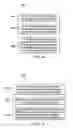
FIGS. 1A and 1B illustrate an example of integrated circuits that employ a printed adhesion deposition material to mitigate integrated circuit delamination.
FIGS. 2A through 2D illustrate an example of a printed adhesion deposition manufacturing process applied to a die attach region of an integrated circuit to mitigate integrated circuit delamination.
FIGS. 3A through 3E illustrate an example of a printed adhesion deposition manufacturing process applied to a lead finger region of an integrated circuit to mitigate integrated circuit delamination.
FIG. 4 illustrates an example of a printed adhesion deposition method for a die attach region of an integrated circuit to mitigate integrated circuit delamination.
FIG. 5 illustrates an example of a printed adhesion perimeter method for a lead finger region of an integrated circuit to mitigate integrated circuit delamination.
DETAILED DESCRIPTION
This disclosure relates to a printed adhesion deposition method to mitigate integrated circuit delamination. Various areas of an integrated circuit can have a printed deposition material applied via an economical printing process such a via an ink jet printer. The printed deposition material can include metal (or metal alloy) nano or micro-particles, where the deposition material mitigates delamination from occurring within the integrated circuit such as at or near the interface between an integrated circuit die and the die pad where the integrated circuit die is mounted. Multi-stage manufacturing methods can be provided that includes applying a die attach material to a die pad of the integrated circuit. The die attach material (e.g., epoxy) is employed as a bonding material to the die pad. This includes mounting the integrated circuit die to the die pad of the integrated circuit via the die attach material. The method then includes printing the adhesion deposition material on the die attach material appearing at the interface of the integrated circuit die and the die pad of the integrated circuit to mitigate delamination between the integrated circuit die and the die pad.
In another aspect, the printed deposition material can be applied to the lead finger area of the integrated circuit. By applying the printed deposition material to the lead finger area, an isolation barrier can be constructed that mitigates contaminants from entering the lead finger area of the integrated circuit. By utilizing the printed deposition material on both the die pad interface and the lead finger areas of the integrated circuit, integrated circuit quality can be improved since delamination is mitigated at the die pad interface and contaminants are reduced from entering the lead finger areas.
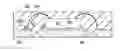
FIGS. 1A and 1B illustrate an example of integrated circuits 100 and 110 that employ a printed adhesion deposition material to mitigate integrated circuit delamination. As used herein, the term circuit can include a collection of active and/or passive elements that perform a circuit function such as an analog circuit or control circuit, for example. The term circuit can also include an integrated circuit where all the circuit elements are fabricated on a common substrate, for example. An integrated circuit die 120 is mounted to a die pad (See e.g., of FIG. 2A for die pad) of the integrated circuit 100. The integrated circuit die 120 can be an analog circuit, digital circuit, or a combination of analog and digital. The integrated circuit die 120 has at least one circuit connection point shown at 124 that can connect via wire 126 to lead finger are 128. An adhesion deposition material (also referred to as first material) 130 is printed along the perimeter of the interface of the integrated circuit die 120 and the die pad of the integrated circuit to mitigate delamination between the integrated circuit die and the die pad. The adhesion deposition material 130 can cover a bonding material 134 that adheres the integrated circuit die 120 to the die pad. The lead finger 128 on the integrated circuit 100 provides external circuit connections to the integrated circuit die 120.
Referring to FIG. 1B and the circuit 110, a second adhesion deposition material such as shown at 140 can be printed along a perimeter of a wire mounting area on a lead finger 144 of the integrated circuit 110. As shown, each lead finger of the circuit 100 can have an area of printed deposition material to mitigate contamination at each area. Also, although not shown, integrated circuits can be manufactured where both the lead finger areas and the integrated circuit die mounting are is coated with the printed deposition material as shown at 130 and 134. The second adhesion deposition material 140 is employed to mitigate contaminants from entering the wire mounting area of the lead finger 144 (or other lead fingers). The integrated circuit 110 includes a conductor such as shown at 150 having a first end bonded to the circuit connection point of the integrated circuit die and a second end bonded to the wire mounting area on the lead finger of the integrated circuit. The second end of the conductor can be bonded within the perimeter defined by the second adhesion deposition material 140. Although rectangular patterns are shown for the printed deposition areas at 130 and 140, substantially any type of pattern can be employed including circular patterns, square patterns, trapezoidal patterns, and so forth depending on the shapes of the lead fingers and or die pad areas, respectively. FIGS. 2A-2D and 3A-3E will now be illustrated and described below that show respective manufacturing processes to apply the printed deposition material to the respective areas for the integrated circuits 100 and/or 110.
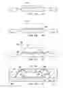
FIGS. 2A through 2D illustrate an example of a printed adhesion deposition manufacturing process applied to a die attach region of an integrated circuit to mitigate integrated circuit delamination. FIG. 2A shows applying a die attach material 204 such as an epoxy to a die pad 208 of an integrated circuit. The die attach material is employed as a bonding material to the die pad 208. FIG. 2B of the manufacturing process includes mounting an integrated circuit die 210 to the die pad 208 of the integrated circuit via the die attach material 204. FIG. 2C of the manufacturing process includes printing an adhesion deposition material such as shown at 220 and 224 via printer 230 on the die attach material appearing at the interface of the integrated circuit die 210 and the die pad 208 of the integrated circuit to mitigate delamination between the integrated circuit die and the die pad. As will be described below with respect to the methods of FIGS. 4 and 5, heating can be applied after the printing. FIG. 2D shows a combined process where wires 240 and 244 are first attached between the die 210 and lead fingers 250 and 254. After the wires are bonded, integrated circuit package molding 260 can be applied.
FIGS. 3A through 3E illustrate an example of a printed adhesion deposition manufacturing process applied to a lead finger region of an integrated circuit to mitigate integrated circuit delamination. FIG. 3A shows applying a die attach material 304 such as an epoxy to a die pad 308 of an integrated circuit. The die attach material is employed as a bonding material to the die pad 308. FIG. 3B of the manufacturing process includes mounting an integrated circuit die 310 to the die pad 308 of the integrated circuit via the die attach material 304. An adhesion deposition material 320 is printed via printer 322 along a perimeter of a wire mounting area 324 on a lead finger 330 of an integrated circuit. The adhesion deposition material is employed to mitigate contaminants and the prorogation of delamination from entering the wire mounting area of the lead finger. FIG. 3D shows bonding an end of a conductor 340 to a connection point on an integrated circuit die 310 and bonding another end of the conductor 340 to the wire mounting area 324 on the lead finger 330 of the integrated circuit within the perimeter defined by the adhesion deposition material. FIG. 3E shows the additional process of applying a molding material 350 to encapsulate the integrated circuit.
In view of the foregoing structural and functional features described above, an example method will be better appreciated with reference to FIGS. 4 and 5. While, for purposes of simplicity of explanation, the methods are shown and described as executing serially, it is to be understood and appreciated that the methods are not limited by the illustrated order, as parts of the methods could occur in different orders and/or concurrently from that shown and described herein. Such methods can be executed to manufacture and integrated circuit, for example.
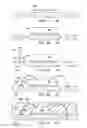
FIG. 4 illustrates an example of a printed adhesion deposition method 400 for a die attach region of an integrated circuit to mitigate integrated circuit delamination. At 410, the method 400 includes applying a die attach material to a die pad of an integrated circuit (See e.g., FIG. 2A). The die attach material is employed as a bonding material to the die pad. At 420, the method 400 includes mounting an integrated circuit die to the die pad of the integrated circuit via the die attach material (See e.g., FIG. 2B). At 430, the method 400 includes printing an adhesion deposition material on the die attach material appearing at the interface of the integrated circuit die and the die pad of the integrated circuit to mitigate delamination between the integrated circuit die and the die pad (See e.g., FIG. 2C).
Although not shown, the method 400 can also include printing the adhesion deposition material via an inkjet printer, a screen printer, or a flexographic printer, for example. The adhesion deposition material can include a metallic particle material that includes nano-particle ink or micro-particle ink, for example. The metallic particle material facilitates an increase of chemical and/or mechanical adhesion at the interface via roughness and/or molecular/atomic forces. The metallic particle material can include a metal and/or a metal alloy. The method 400 can also include heating the adhesion deposition material during or after the printing of the adhesion deposition material. The heating can be applied via laser, flash lamp, infrared, or plasma, microwave, for example. The heating can be in the range of about 80 degrees Celsius to about 200 degrees Celsius, for example. The method 400 can also include bonding at least one wire between the integrated circuit and a lead finger that provides external connections to the integrated circuit. This includes applying a molding material to the integrated circuit to encapsulate the integrated circuit.
FIG. 5 illustrates an example of a printed adhesion perimeter method 500 for a lead finger region of an integrated circuit to mitigate integrated circuit delamination. At 510, the method 500 includes printing an adhesion deposition material along a perimeter of a wire mounting area on a lead finger of an integrated circuit (See e.g., FIG. 3C). The adhesion deposition material is employed to mitigate contaminants from entering the wire mounting area of the lead finger. At 520, the method 500 includes bonding an end of a conductor to a connection point on an integrated circuit die (See e.g., FIG. 3D). At 530, the method 500 includes bonding another end of the conductor to the wire mounting area on the lead finger of the integrated circuit within the perimeter defined by the adhesion deposition material (See e.g., FIG. 3D).
Although not shown, the method 500 can also include printing the adhesion deposition material via an inkjet printer, a screen printer, or a flexographic printer, for example. The adhesion deposition material includes a metallic particle material that includes nano-particle ink or micro-particle ink, for example. The metallic particle material includes a metal or a metal alloy. The method 500 can also include heating the adhesion deposition material during or after the printing of the adhesion deposition material. Similar to the method 400, the method 500 can include heating in the range of about 80 degrees Celsius to about 200 degrees Celsius. The method 500 can also include applying a molding material to the integrated circuit to encapsulate the integrated circuit.
What have been described above are examples. It is, of course, not possible to describe every conceivable combination of components or methodologies, but one of ordinary skill in the art will recognize that many further combinations and permutations are possible. Accordingly, the disclosure is intended to embrace all such alterations, modifications, and variations that fall within the scope of this application, including the appended claims. As used herein, the term “includes” means includes but not limited to, the term “including” means including but not limited to. The term “based on” means based at least in part on. Additionally, where the disclosure or claims recite “a,” “an,” “a first,” or “another” element, or the equivalent thereof, it should be interpreted to include one or more than one such element, neither requiring nor excluding two or more such elements.
Claims
What is claimed is:1. A method, comprising:
applying a die attach material to a die pad of an integrated circuit, the die attach material employed as a bonding material to the die pad;
mounting an integrated circuit die to the die pad of the integrated circuit via the die attach material; and
printing an adhesion deposition material on the die attach material appearing at the interface of the integrated circuit die and the die pad of the integrated circuit to mitigate delamination between the integrated circuit die and the die pad.
2. The method of claim 1, further comprising printing the adhesion deposition material via an inkjet printer, a screen printer, or a flexographic printer.
3. The method of claim 1, wherein the adhesion deposition material includes a metallic particle material that includes nano-particle ink or micro-particle ink.
4. The method of claim 3, wherein the metallic particle material includes a metal or a metal alloy.
5. The method of claim 1, further comprising heating the adhesion deposition material during or after the printing of the adhesion deposition material, where the heating can be applied via laser, flash lamp, infrared, or plasma, microwave.
6. The method of claim 5, wherein the heating is in the range of about 80 degrees Celsius to about 200 degrees Celsius.
7. The method of claim of claim 6, further comprising bonding at least one wire between the integrated circuit and a lead finger that provides external connections to the integrated circuit.
8. The method of claim 7, further comprising applying a molding material to the integrated circuit to encapsulate the integrated circuit.
9. A method, comprising:
printing an adhesion deposition material along a perimeter of a wire mounting area on a lead finger of an integrated circuit, the adhesion deposition material employed to mitigate contaminants from entering the wire mounting area of the lead finger;
bonding an end of a conductor to a connection point on an integrated circuit die; and
bonding another end of the conductor to the wire mounting area on the lead finger of the integrated circuit within the perimeter defined by the adhesion deposition material.
10. The method of claim 9, further comprising printing the adhesion deposition material via an inkjet printer, a screen printer, or a flexographic printer.
11. The method of claim 9, wherein the adhesion deposition material includes a metallic particle material that includes nano-particle ink or micro-particle ink.
12. The method of claim 11, wherein the metallic particle material includes a metal or a metal alloy.
13. The method of claim 9, further comprising heating the adhesion deposition material during or after the printing of the adhesion deposition material.
14. The method of claim 13, wherein the heating is in the range of about 80 degrees Celsius to about 200 degrees Celsius.
15. The method of claim 14, further comprising applying a molding material to the integrated circuit to encapsulate the integrated circuit.
16. An integrated circuit, comprising:
a die pad of the integrated circuit;
an integrated circuit die mounted to the die pad of the integrated circuit, the integrated circuit die having a circuit connection point;
a first adhesion deposition material printed along the perimeter of the interface of the integrated circuit die and the die pad of the integrated circuit to mitigate delamination between the integrated circuit die and the die pad;
a lead finger on the integrated circuit to provide external circuit connections to the integrated circuit die;
a second adhesion deposition material printed along a perimeter of a wire mounting area on the lead finger of the integrated circuit, the second adhesion deposition material employed to mitigate contaminants from entering the wire mounting area of the lead finger; and
a conductor having a first end bonded to the circuit connection point of the integrated circuit die and a second end bonded to the wire mounting area on the lead finger of the integrated circuit, the second end of the conductor bonded within the perimeter defined by the second adhesion deposition material.
17. The circuit of claim 16, wherein the first and second adhesion deposition materials are printed via an inkjet printer, a screen printer, or a flexographic printer.
18. The circuit of claim 16, wherein the adhesion deposition material includes a metallic particle material that includes nano-particle ink or micro-particle ink and the metallic particle material includes a metal or a metal alloy.
19. The circuit of claim 16, wherein the adhesion deposition material is heated during or after the printing of the adhesion deposition material.
20. The circuit of claim 19, wherein the adhesion deposition material is heated in the range of about 80 degrees Celsius to about 200 degrees Celsius.
Images & Drawings included:
Sources:
- United States Patent and Trademark Office - verify current appl. status at the USPTO↗
Recent applications in this class:
- » 20250105025 2025-03-27
BLANKET WAFER LASER PRE-EXPOSURE FOR FAST SELECTIVE LAYER TRANSFERS - » 20240363367 2024-10-31
METHOD FOR PRODUCING AN ELECTRONIC COMPONENT, AND ELECTRONIC COMPONENT - » 20240274442 2024-08-15
SEMICONDUCTOR DEVICE AND METHOD OF MANUFACTURING THE SAME - » 20230386862 2023-11-30
SEMICONDUCTOR DEVICE AND METHOD OF MANUFACTURE - » 20230230853 2023-07-20
MANUFACTURING APPARATUS AND MANUFACTURING METHOD OF SEMICONDUCTOR DEVICE - » 20230197468 2023-06-22
METHOD FOR MANUFACTURING A POWER SEMICONDUCTOR MODULE AND POWER SEMICONDUCTOR MODULE - » 20230110154 2023-04-13
SEMICONDUCTOR DEVICE - » 20230047789 2023-02-16
Semiconductor device and method of manufacturing semiconductor device - » 20220216071 2022-07-07
Semiconductor device and method of manufacture - » 20220068665 2022-03-03
Semiconductor device package and method of manufacturing the same
Recent applications for this Assignee:
- » 20250291595 2025-09-18
CIRCUIT, SYSTEM, AND METHOD FOR MATRIX DECIMATION - » 20250286550 2025-09-11
TRANSISTOR SHUTDOWN CIRCUT - » 20250279725 2025-09-04
CONDUCTION MODE CONTROL - » 20250274138 2025-08-28
SWITCH REGULATOR - » 20250267687 2025-08-21
ENHANCED BROADCAST TRANSMISSION IN UNSLOTTED CHANNEL HOPPING MEDIUM ACCESS CONTROL - » 20250266825 2025-08-21
BOOTSTRAP CIRCUIT - » 20250247097 2025-07-31
LEVEL SHIFTER CIRCUIT - » 20250247082 2025-07-31
LOW AREA AND POWER MULTI-BIT FLIP-FLOP - » 20250246995 2025-07-31
SWITCHING CONVERTER DEADTIME CONTROL - » 20250246345 2025-07-31
TRIMMING RESISTOR USING MODULATED SIGNAL