Pixel compensation circuits, scanning driving circuits and flat display devices
US20180040277A1
2018-02-08
15/024,578
2016-02-25
✅ Patent granted
US 10,192,482 B2
2019-01-29
WO; PCT/CN2016/074529; 20160225
WO; WO2017/128465; 20170803
Premal R Patel
Andrew C. Cheng
2036-08-25
Abstract:
The present disclosure relates to a pixel compensation circuit, a scanning driving circuit and a flat display device. Control end of first controllable transistor connects to first scanning line, first end of first controllable transistor connects to data line; control end of driving transistor connects to second end of first controllable transistor, first end of driving transistor connects to first voltage end; control end of second controllable transistor connects to second scanning line, first end of second controllable transistor connects to second end of driving transistor; anode of OLED connects to second end of second controllable transistor, cathode of OLED is grounded; control end of driving transistor connects to first end of second controllable transistor through first capacitor, first end of second controllable transistor connects to second voltage end through second capacitor.
Inventors:
- Yuying CAI 8 🇨🇳 Shenzhen, Guangdong, China
- Kaiyuan KE 1 🇨🇳 Shenzhen, Guangdong, China
- Yuying Cai 8 🇨🇳 Guangdong, China
- Kaiyuan Ke 1 🇨🇳 Guangdong, China
Assignee:
- Shenzhen China Star Optoelectronics Technology Co Ltd. 3,202 🇨🇳 Shenzhen, Guangdong, China
Applicant:
Interested in similar patents?
Get notified when new applications in this technology area are published.
Classification:
G09G3/3266 » CPC further
Control arrangements or circuits, of interest only in connection with visual indicators other than cathode-ray tubes for presentation of an assembly of a number of characters, e.g. a page, by composing the assembly by combination of individual elements arranged in a matrix no fixed position being assigned to or needed to be assigned to the individual characters or partial characters using controlled light sources using electroluminescent panels semiconductive, e.g. using light-emitting diodes [LED] organic, e.g. using organic light-emitting diodes [OLED] Details of drivers for scan electrodes
G09G3/3677 » CPC further
Control arrangements or circuits, of interest only in connection with visual indicators other than cathode-ray tubes for presentation of an assembly of a number of characters, e.g. a page, by composing the assembly by combination of individual elements arranged in a matrix no fixed position being assigned to or needed to be assigned to the individual characters or partial characters by control of light from an independent source using liquid crystals; Control of matrices with row and column drivers; Details of drivers for scan electrodes suitable for active matrices only
G09G3/3688 » CPC further
Control arrangements or circuits, of interest only in connection with visual indicators other than cathode-ray tubes for presentation of an assembly of a number of characters, e.g. a page, by composing the assembly by combination of individual elements arranged in a matrix no fixed position being assigned to or needed to be assigned to the individual characters or partial characters by control of light from an independent source using liquid crystals; Control of matrices with row and column drivers; Details of drivers for data electrodes suitable for active matrices only
G09G3/36 IPC
Control arrangements or circuits, of interest only in connection with visual indicators other than cathode-ray tubes for presentation of an assembly of a number of characters, e.g. a page, by composing the assembly by combination of individual elements arranged in a matrix no fixed position being assigned to or needed to be assigned to the individual characters or partial characters by control of light from an independent source using liquid crystals
G09G2300/0819 » CPC further
Aspects of the constitution of display devices; Active matrix structure, i.e. with use of active elements, inclusive of non-linear two terminal elements, in the pixels together with light emitting or modulating elements; Several active elements per pixel in active matrix panels used for counteracting undesired variations, e.g. feedback or autozeroing
G09G2300/0842 » CPC further
Aspects of the constitution of display devices; Active matrix structure, i.e. with use of active elements, inclusive of non-linear two terminal elements, in the pixels together with light emitting or modulating elements; Several active elements per pixel in active matrix panels forming a memory circuit, e.g. a dynamic memory with one capacitor
G09G2300/0861 » CPC further
Aspects of the constitution of display devices; Active matrix structure, i.e. with use of active elements, inclusive of non-linear two terminal elements, in the pixels together with light emitting or modulating elements; Several active elements per pixel in active matrix panels forming a memory circuit, e.g. a dynamic memory with one capacitor with additional control of the display period without amending the charge stored in a pixel memory, e.g. by means of additional select electrodes
G09G2310/0283 » CPC further
Command of the display device; Addressing, scanning or driving the display screen or processing steps related thereto; Details of driving circuits Arrangement of drivers for different directions of scanning
G09G2310/08 » CPC further
Command of the display device Details of timing specific for flat panels, other than clock recovery
Description
BACKGROUND OF THE INVENTION
1. Field of the Invention
The present disclosure relates to display technology, and more particularly to a pixel compensation circuit, a scanning driving circuit, and a flat display device.
2. Discussion of the Related Art
Organic light emitting diode (OLED) displays are characterized by attributes such as small dimensional, simple structure, emitting light itself, large viewing angle, and short response time, and thus have drew a great deal attentions. The voltage signals outputted by the first voltage end and the data voltage signals outputted from the data line of the OLED display are complex, and may cause adverse impact toward the circuit operations.
SUMMARY
The present disclosure relates to a pixel compensation circuit, a scanning driving circuit and a flat display device to reduce the complexity of the voltage signals outputted by the first voltage end and the data voltage signals outputted from the data line of the OLED display so as to facilitate the operations of the circuit.
In one aspect, a pixel compensation circuit includes: a first controllable transistor having a control end, a first end, and a second end, the control end of the first controllable transistor connects to a first scanning line, and the first end of the first controllable transistor connects to one data line to receive a data voltage via the data line; a driving transistor having a control end, a first end, and a second end, the control end of the driving transistor connects to the second end of the first controllable transistor, and the first end of the driving transistor connects to a first voltage end; a second controllable transistor having a control end, a first end, and a second end, the control end of the second controllable transistor connects to a second scanning line, and the first end of the second controllable transistor connects to the second end of the driving transistor; an OLED having an anode and a cathode, the anode of the OLED connects to the second end of the second controllable transistor, and the cathode of the OLED is grounded; a first capacitor having a first end and a second end, the first end of the first capacitor connects to the control end of the driving transistor, and the second end of the first capacitor connects to the first end of the second controllable transistor; and a second capacitor includes a first end and a second end, the first end of the second capacitor connects to the first end of the second controllable transistor and the second end of the first capacitor, and the second end of the second capacitor connects to a second voltage end.
Wherein the driving transistor, the first controllable transistor, and the second controllable transistor are NMOS TFTs, or PMOS TFTs, or a combination of NMOS TFTs and PMOS TFTs, and the control end, the first end, and the second end of the driving transistor, the first controllable transistor, and the second controllable transistor respectively correspond to a gate, a drain, and a source of a TFT.
In one aspect, a scanning driving circuit includes a pixel compensation circuit, and the pixel compensation circuit includes: a first controllable transistor having a control end, a first end, and a second end, the control end of the first controllable transistor connects to a first scanning line, and the first end of the first controllable transistor connects to one data line to receive a data voltage via the data line; a driving transistor having a control end, a first end, and a second end, the control end of the driving transistor connects to the second end of the first controllable transistor, and the first end of the driving transistor connects to a first voltage end; a second controllable transistor having a control end, a first end, and a second end, the control end of the second controllable transistor connects to a second scanning line, and the first end of the second controllable transistor connects to the second end of the driving transistor; an OLED having an anode and a cathode, the anode of the OLED connects to the second end of the second controllable transistor, and the cathode of the OLED is grounded; a first capacitor having a first end and a second end, the first end of the first capacitor connects to the control end of the driving transistor, and the second end of the first capacitor connects to the first end of the second controllable transistor; and a second capacitor includes a first end and a second end, the first end of the second capacitor connects to the first end of the second controllable transistor and the second end of the first capacitor, and the second end of the second capacitor connects to a second voltage end.
Wherein the driving transistor, the first controllable transistor, and the second controllable transistor are NMOS TFTs, or PMOS TFTs, or a combination of NMOS TFTs and PMOS TFTs, and the control end, the first end, and the second end of the driving transistor, the first controllable transistor, and the second controllable transistor respectively correspond to a gate, a drain, and a source of a TFT.
In another aspect, a flat display device includes a pixel compensation circuit, and the pixel compensation circuit includes: a first controllable transistor having a control end, a first end, and a second end, the control end of the first controllable transistor connects to a first scanning line, and the first end of the first controllable transistor connects to one data line to receive a data voltage via the data line; a driving transistor having a control end, a first end, and a second end, the control end of the driving transistor connects to the second end of the first controllable transistor, and the first end of the driving transistor connects to a first voltage end; a second controllable transistor having a control end, a first end, and a second end, the control end of the second controllable transistor connects to a second scanning line, and the first end of the second controllable transistor connects to the second end of the driving transistor; an OLED having an anode and a cathode, the anode of the OLED connects to the second end of the second controllable transistor, and the cathode of the OLED is grounded; a first capacitor having a first end and a second end, the first end of the first capacitor connects to the control end of the driving transistor, and the second end of the first capacitor connects to the first end of the second controllable transistor; and a second capacitor includes a first end and a second end, the first end of the second capacitor connects to the first end of the second controllable transistor and the second end of the first capacitor, and the second end of the second capacitor connects to a second voltage end.
Wherein the driving transistor, the first controllable transistor, and the second controllable transistor are NMOS TFTs, or PMOS TFTs, or a combination of NMOS TFTs and PMOS TFTs, and the control end, the first end, and the second end of the driving transistor, the first controllable transistor, and the second controllable transistor respectively correspond to a gate, a drain, and a source of a TFT.
Wherein the flat display device is an OLED or LCD.
In view of the above, the pixel compensation circuit adopts the second controllable transistor (T2), the second capacitor (C2), and the second voltage end to reduce the complexity of the first voltage signals outputted by the first voltage end and the data voltage signals outputted from the data line so as to facilitate the operations of the circuit.
BRIEF DESCRIPTION OF THE DRAWINGS
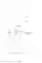
FIG. 1 is a schematic view of one conventional pixel compensation circuit.
FIG. 2 is a waveform diagram of one conventional pixel compensation circuit.
FIG. 3 is a simulation diagram of one conventional pixel compensation circuit.
FIG. 4 is a schematic view of the pixel compensation circuit in accordance with one embodiment.
FIG. 5 is a waveform diagram of the pixel compensation circuit in accordance with one embodiment.
FIG. 6 is a simulation diagram of the pixel compensation circuit in accordance with one embodiment.
FIG. 7 is a schematic view of the scanning driving circuit in accordance with one embodiment.
FIG. 8 is a schematic view of the flat display device in accordance with one embodiment.
DETAILED DESCRIPTION OF THE EMBODIMENTS
Embodiments of the invention will now be described more fully hereinafter with reference to the accompanying drawings, in which embodiments of the invention are shown.
Referring to FIGS. 1-3, the conventional pixel compensation circuit includes two thin film transistors (TFTs) and one storage capacitor. During the compensation phase, the current of the pixel compensation circuit passes through the OLEDs. In view of FIG. 2, the voltage (VDD) signals outputted from the first voltage end of the pixel compensation circuit are complex and the signals are delayed. In addition, the data voltage (Vdata) may affect the voltage of second end of the driven transistor, and the data voltage (Vdata) signals are complex.
FIG. 4 is a schematic view of the pixel compensation circuit in accordance with one embodiment. As shown in FIG. 4, the controllable includes:
A first controllable transistor (T1) includes a control end, a first end, and a second end. The control end of the first controllable transistor (T1) connects to a first scanning line (Vsl), and the first end of the first controllable transistor (T1) connects to one data line (Data) such that the data line (Data) receives the data voltage (Vdata);
A driving transistor (T0) includes a control end, a first end, and a second end. The control end of the driving transistor (T0) connects to the second end of the first controllable transistor (T1), and the first end of the driving transistor (T0) connects to the first voltage end (VDD1);
A second controllable transistor (T2) includes a control end, a first end, and a second end. The control end of the second controllable transistor (T2) connects to a second scanning line (Vg1), and the first end of the second controllable transistor (T2) connects to the second end of the driving transistor (T0);
An OLED (D1) having an anode and a cathode. The anode of the OLED (D1) connects to the second end of the second controllable transistor (T2), and the cathode of the OLED (D1) is grounded;
A first capacitor (C1) includes a first end and a second end. The first end of the first capacitor (C1) connects to the control end of the driving transistor (T0), and the second end of the first capacitor (C1) connects to the first end of the second controllable transistor (T2); and
A second capacitor (C2) includes a first end and a second end. The first end of the second capacitor (C2) connects to the first end of the second controllable transistor (T2) and the second end of the first capacitor (C1), and the second end of the second capacitor (C2) connects to a second voltage end (R).
In the embodiment, the driving transistor (T0), the first controllable transistor (T1), and the second controllable transistor (T2) are NMOS TFTs, or PMOS TFTs, or a combination of NMOS TFTs and PMOS TFTs. The control end, the first end, and the second end of the driving transistor (T0), the first controllable transistor (T1), and the second controllable transistor (T2) respectively correspond to a gate, a drain, and a source of the TFT.
FIG. 5 is a waveform diagram of the pixel compensation circuit in accordance with one embodiment. FIG. 6 is a simulation diagram of the pixel compensation circuit in accordance with one embodiment. As shown, the second controllable transistor (T2) prevents the current from passing through the OLED (D1) during a compensation phase. In FIG. 4, it can be clear that the complexity of the first voltage (VDD) signals has been reduced, and the delay has also been decreased. In response to the control of the second capacitor (C2) and the second voltage end (R), the impact from the data voltage (Vdata) toward the voltage at two ends of the driving transistor (T0) has been reduced. In addition, it can be clearly seen that the complexity of the data voltage (Vdata) signals is also reduced in view of FIG. 4.
FIG. 7 is a schematic view of the scanning driving circuit in accordance with one embodiment. The scanning driving circuit includes the above pixel compensation circuit for avoiding the threshold voltage drifting with respect to the driving transistor within the scanning driving circuit so as to avoid the non-uniform brightness of the panel.
FIG. 8 is a schematic view of the flat display device in accordance with one embodiment. The flat display device may be OLED or LCD including the above scanning driving circuit and the above pixel compensation circuit. The scanning driving circuit having the pixel compensation circuit is arranged in a rim of the flat display device. In an example, the scanning driving circuits are arranged at two ends of the flat display device.
The pixel compensation circuit adopts the second controllable transistor (T2), the second capacitor (C2), and the second voltage end to reduce the complexity of the first voltage signals outputted by the first voltage end and the data voltage signals outputted from the data line so as to facilitate the operations of the circuit.
It is believed that the present embodiments and their advantages will be understood from the foregoing description, and it will be apparent that various changes may be made thereto without departing from the spirit and scope of the invention or sacrificing all of its material advantages, the examples hereinbefore described merely being preferred or exemplary embodiments of the invention.
Claims
What is claimed is:1. A pixel compensation circuit, comprising:
a first controllable transistor having a control end, a first end, and a second end, the control end of the first controllable transistor connects to a first scanning line, and the first end of the first controllable transistor connects to one data line to receive a data voltage via the data line;
a driving transistor having a control end, a first end, and a second end, the control end of the driving transistor connects to the second end of the first controllable transistor, and the first end of the driving transistor connects to a first voltage end;
a second controllable transistor having a control end, a first end, and a second end, the control end of the second controllable transistor connects to a second scanning line, and the first end of the second controllable transistor connects to the second end of the driving transistor;
an OLED having an anode and a cathode, the anode of the OLED connects to the second end of the second controllable transistor, and the cathode of the OLED is grounded;
a first capacitor having a first end and a second end, the first end of the first capacitor connects to the control end of the driving transistor, and the second end of the first capacitor connects to the first end of the second controllable transistor; and
a second capacitor includes a first end and a second end, the first end of the second capacitor connects to the first end of the second controllable transistor and the second end of the first capacitor, and the second end of the second capacitor connects to a second voltage end.
2. The pixel compensation circuit as claimed in claim 1, wherein the driving transistor, the first controllable transistor, and the second controllable transistor are NMOS TFTs, or PMOS TFTs, or a combination of NMOS TFTs and PMOS TFTs, and the control end, the first end, and the second end of the driving transistor, the first controllable transistor, and the second controllable transistor respectively correspond to a gate, a drain, and a source of a TFT.
3. A scanning driving circuit comprises a pixel compensation circuit, and the pixel compensation circuit comprising:
a first controllable transistor having a control end, a first end, and a second end, the control end of the first controllable transistor connects to a first scanning line, and the first end of the first controllable transistor connects to one data line to receive a data voltage via the data line;
a driving transistor having a control end, a first end, and a second end, the control end of the driving transistor connects to the second end of the first controllable transistor, and the first end of the driving transistor connects to a first voltage end;
a second controllable transistor having a control end, a first end, and a second end, the control end of the second controllable transistor connects to a second scanning line, and the first end of the second controllable transistor connects to the second end of the driving transistor;
an OLED having an anode and a cathode, the anode of the OLED connects to the second end of the second controllable transistor, and the cathode of the OLED is grounded;
a first capacitor having a first end and a second end, the first end of the first capacitor connects to the control end of the driving transistor, and the second end of the first capacitor connects to the first end of the second controllable transistor; and
a second capacitor includes a first end and a second end, the first end of the second capacitor connects to the first end of the second controllable transistor and the second end of the first capacitor, and the second end of the second capacitor connects to a second voltage end.
4. The scanning driving circuit as claimed in claim 3, wherein the driving transistor, the first controllable transistor, and the second controllable transistor are NMOS TFTs, or PMOS TFTs, or a combination of NMOS TFTs and PMOS TFTs, and the control end, the first end, and the second end of the driving transistor, the first controllable transistor, and the second controllable transistor respectively correspond to a gate, a drain, and a source of a TFT.
5. A flat display device comprises a pixel compensation circuit, and the pixel compensation circuit comprising:
a first controllable transistor having a control end, a first end, and a second end, the control end of the first controllable transistor connects to a first scanning line, and the first end of the first controllable transistor connects to one data line to receive a data voltage via the data line;
a driving transistor having a control end, a first end, and a second end, the control end of the driving transistor connects to the second end of the first controllable transistor, and the first end of the driving transistor connects to a first voltage end;
a second controllable transistor having a control end, a first end, and a second end, the control end of the second controllable transistor connects to a second scanning line, and the first end of the second controllable transistor connects to the second end of the driving transistor;
an OLED having an anode and a cathode, the anode of the OLED connects to the second end of the second controllable transistor, and the cathode of the OLED is grounded;
a first capacitor having a first end and a second end, the first end of the first capacitor connects to the control end of the driving transistor, and the second end of the first capacitor connects to the first end of the second controllable transistor; and
a second capacitor includes a first end and a second end, the first end of the second capacitor connects to the first end of the second controllable transistor and the second end of the first capacitor, and the second end of the second capacitor connects to a second voltage end.
6. The flat display device as claimed in claim 5, wherein the driving transistor, the first controllable transistor, and the second controllable transistor are NMOS TFTs, or PMOS TFTs, or a combination of NMOS TFTs and PMOS TFTs, and the control end, the first end, and the second end of the driving transistor, the first controllable transistor, and the second controllable transistor respectively correspond to a gate, a drain, and a source of a TFT.
7. The flat display device as claimed in claim 5, wherein the flat display device is an OLED or LCD.
Images & Drawings included:


Sources:
- United States Patent and Trademark Office - verify current appl. status at the USPTO↗
Similar patent applications:
Recent applications in this class:
- » 20250292736 2025-09-18
DRIVING CIRCUIT, DRIVING METHOD, DRIVING MODULE AND DISPLAY DEVICE - » 20250292735 2025-09-18
DISPLAY DEVICE WHOSE DUTY RATIO IN SUB-FRAME PERIOD IS CONTROLLED - » 20250285596 2025-09-11
PIXEL AND DISPLAY DEVICE INCLUDING THE SAME - » 20250285595 2025-09-11
DISPLAY DEVICE - » 20250279060 2025-09-04
DISPLAY SUBSTRATE AND DISPLAY DEVICE - » 20250279059 2025-09-04
DISPLAY DRIVING CIRCUIT AND DISPLAY DEVICE INCLUDING THE SAME - » 20250273157 2025-08-28
DISPLAY DEVICE AND METHOD OF DRIVING THE SAME - » 20250266000 2025-08-21
VOLTAGE-INPUT PIXEL DRIVING CIRCUIT FOR MICRODISPLAY PANEL - » 20250259600 2025-08-14
DRIVING CIRCUIT, DRIVING METHOD, DRIVING MODULE AND DISPLAY DEVICE - » 20250246147 2025-07-31
METHODS OF COMPENSATING DISPLAY PANEL FOR REDUCING LUMINANCE DISCREPANCY
Recent applications for this Assignee:
- » 20200355948 2020-11-12
FRAME SEALANT AND LIQUID CRYSTAL DISPLAY PANEL - » 20200341310 2020-10-29
Thin film transistor liquid crystal display (TFT-LCD) and the driving circuit and switching power supply thereof - » 20200285088 2020-09-10
Array substrate of thin-film transistor liquid crystal display device and method for manufacturing the same - » 20200272004 2020-08-27
Array substrate and liquid crystal display panel - » 20200258866 2020-08-13
Display panel, manufacturing method thereof and display device - » 20200251055 2020-08-06
Brightness regulation device of display device, brightness regulation method and display device - » 20200201464 2020-06-25
Array substrate and touch display device - » 20200185452 2020-06-11
Manufacturing method of micro light-emitting diode display panel - » 20200181759 2020-06-11
VAPOR DEPOSITION CRUCIBLE - » 20200168842 2020-05-28
Organic light-emitting diode (OLED) display panel and manufacturing method thereof