Flexible substrate, flexible display panel, and manufacturing method thereof
US20210359232A1
2021-11-18
16/472,974
2019-03-19
✅ Patent granted
US 11,283,032 B2
2022-03-22
WO; PCT/CN2019/078750; 20190319
WO; WO2020/118953; 20200618
Victoria K. Hall
2040-07-09
Abstract:
A flexible substrate, a flexible display panel, and a manufacturing method are provided. The method of manufacturing the flexible display panel includes forming a first organic layer on a substrate; determining a bending area on the first organic layer and forming an adhesion layer on a part of the first organic layer, located in the bending area; forming an inorganic layer on the adhesion layer and on the first organic layer; forming a second organic layer on the inorganic layer; forming a thin-film transistor layer, an organic light-emitting diode layer, and an encapsulation layer on the second organic layer in sequence; removing the substrate; and removing the part of the first organic layer, located in the bending area, and the adhesion layer so that the flexible display panel is formed.
Assignee:
- WUHAN CHINA STAR OPTOELECTRONICS SEMICONDUCTOR DISPLAY TECHNOLOGY CO., LTD. 607 🇨🇳 Hubei, China
Applicant:
Interested in similar patents?
Get notified when new applications in this technology area are published.
Classification:
B32B37/24 » CPC further
Methods or apparatus for laminating, e.g. by curing or by ultrasonic bonding characterised by the properties of the layers with at least one layer not being coherent before laminating, e.g. made up from granular material sprinkled onto a substrate
H01L27/3244 » CPC further
Devices consisting of a plurality of semiconductor or other solid-state components formed in or on a common substrate including components using organic materials as the active part, or using a combination of organic materials with other materials as the active part with components specially adapted for light emission, e.g. flat-panel displays using organic light-emitting diodes [OLED]; Matrix-type displays Active matrix displays
H01L51/003 » CPC further
Solid state devices using organic materials as the active part, or using a combination of organic materials with other materials as the active part; Processes or apparatus specially adapted for the manufacture or treatment of such devices, or of parts thereof; Processes specially adapted for the manufacture or treatment of devices or of parts thereof using a temporary substrate
B32B2255/10 » CPC further
Coating on the layer surface on synthetic resin layer or on natural or synthetic rubber layer
B32B2255/20 » CPC further
Coating on the layer surface Inorganic coating
B32B27/281 » CPC further
Layered products comprising synthetic resin comprising synthetic resins not wholly covered by any one of the sub-groups - comprising polyimides
B32B2457/20 » CPC further
Electrical equipment Displays, e.g. liquid crystal displays, plasma displays
H01L2251/5338 » CPC further
Indexing scheme relating to organic semiconductor devices covered by group; Organic light emitting devices; Structure Flexible OLED
H01L51/00 IPC
Solid state devices using organic materials as the active part, or using a combination of organic materials with other materials as the active part; Processes or apparatus specially adapted for the manufacture or treatment of such devices, or of parts thereof
H01L27/32 IPC
Devices consisting of a plurality of semiconductor or other solid-state components formed in or on a common substrate including components using organic materials as the active part, or using a combination of organic materials with other materials as the active part with components specially adapted for light emission, e.g. flat-panel displays using organic light-emitting diodes [OLED]
H01L51/56 » CPC further
Solid state devices using organic materials as the active part, or using a combination of organic materials with other materials as the active part; Processes or apparatus specially adapted for the manufacture or treatment of such devices, or of parts thereof specially adapted for light emission, e.g. organic light emitting diodes [OLED] or polymer light emitting devices [PLED] Processes or apparatus specially adapted for the manufacture or treatment of such devices or of parts thereof
B32B2037/243 » CPC further
Methods or apparatus for laminating, e.g. by curing or by ultrasonic bonding characterised by the properties of the layers with at least one layer not being coherent before laminating, e.g. made up from granular material sprinkled onto a substrate Coating
B32B37/12 » CPC further
Methods or apparatus for laminating, e.g. by curing or by ultrasonic bonding characterised by using adhesives
H05K1/118 » CPC further
Printed circuits; Details; Printed elements for providing electric connections to or between printed circuits specially for flexible printed circuits, e.g. using folded portions
H05K1/118 » CPC further
Printed circuits; Details; Printed elements for providing electric connections to or between printed circuits specially for flexible printed circuits, e.g. using folded portions
B32B3/28 » CPC further
Layered products comprising a layer with external or internal discontinuities or unevennesses, or a layer of non-planar form ; Layered products having particular features of form characterised by a particular shape of the outline of the cross-section of a continuous layer; characterised by a layer with cavities or internal voids ; characterised by an apertured layer characterised by a layer comprising a deformed thin sheet, i.e. the layer having its entire thickness deformed out of the plane , e.g. corrugated, crumpled
B32B7/022 » CPC further
Layered products characterised by the relation between layers; Layered products characterised by the relative orientation of features between layers, or by the relative values of a measurable parameter between layers, i.e. products comprising layers having different physical, chemical or physicochemical properties; Layered products characterised by the interconnection of layers; Physical, chemical or physicochemical properties Mechanical properties
B32B3/30 » CPC further
Layered products comprising a layer with external or internal discontinuities or unevennesses, or a layer of non-planar form ; Layered products having particular features of form characterised by a particular shape of the outline of the cross-section of a continuous layer; characterised by a layer with cavities or internal voids ; characterised by an apertured layer characterised by a layer formed with recesses or projections, e.g. hollows, grooves, protuberances, ribs
B32B2457/206 » CPC further
Electrical equipment; Displays, e.g. liquid crystal displays, plasma displays Organic displays, e.g. OLED
H01L2227/326 » CPC further
Indexing scheme for devices consisting of a plurality of semiconductor or other solid state components formed in or on a common substrate covered by group; Devices including an organic light emitting device [OLED], e.g. OLED display Use of temporary substrate, e.g. for manufacturing of OLED displays having an inorganic driving circuit
B32B7/05 » CPC further
Layered products characterised by the relation between layers; Layered products characterised by the relative orientation of features between layers, or by the relative values of a measurable parameter between layers, i.e. products comprising layers having different physical, chemical or physicochemical properties; Layered products characterised by the interconnection of layers; Interconnection of layers the layers not being connected over the whole surface, e.g. discontinuous connection or patterned connection
H05K1/028 » CPC further
Printed circuits; Details; Bendability or stretchability details Bending or folding regions of flexible printed circuits
H05K1/028 » CPC further
Printed circuits; Details; Bendability or stretchability details Bending or folding regions of flexible printed circuits
H05K1/02 IPC
Printed circuits Details
H05K1/02 IPC
Printed circuits Details
H05K1/11 IPC
Printed circuits; Details Printed elements for providing electric connections to or between printed circuits
H05K1/11 IPC
Printed circuits; Details Printed elements for providing electric connections to or between printed circuits
H05K2201/055 » CPC further
Indexing scheme relating to printed circuits covered by; Flexible printed circuits [FPCs] Folded back on itself
H05K2201/055 » CPC further
Indexing scheme relating to printed circuits covered by; Flexible printed circuits [FPCs] Folded back on itself
H01L51/0097 » CPC main
Solid state devices using organic materials as the active part, or using a combination of organic materials with other materials as the active part; Processes or apparatus specially adapted for the manufacture or treatment of such devices, or of parts thereof; Substrates flexible substrates
B32B7/12 » CPC further
Layered products characterised by the relation between layers; Layered products characterised by the relative orientation of features between layers, or by the relative values of a measurable parameter between layers, i.e. products comprising layers having different physical, chemical or physicochemical properties; Layered products characterised by the interconnection of layers; Interconnection of layers using interposed adhesives or interposed materials with bonding properties
B32B27/08 » CPC further
Layered products comprising synthetic resin as the main or only constituent of a layer, next to another layer of a of synthetic resin
H05K2201/10128 » CPC further
Indexing scheme relating to printed circuits covered by; Details of components or other objects attached to or integrated in a printed circuit board; Types of components Display
H05K2201/10128 » CPC further
Indexing scheme relating to printed circuits covered by; Details of components or other objects attached to or integrated in a printed circuit board; Types of components Display
B32B27/28 IPC
Layered products comprising synthetic resin comprising synthetic resins not wholly covered by any one of the sub-groups -
Description
BACKGROUND OF DISCLOSURE
1. Field of Disclosure
The present invention relates to the field of display technology, and more particularly, to a flexible substrate, a flexible display panel, and a manufacturing method thereof.
2. Description of Related Art
In recent years, there has been an increasing interest in full screen display devices. To organic light-emitting diode (OLED) display panels, pad bending technology can realize full screen effects through bending a bonding area of a flexible substrate in which a control chip is bonded to be behind a display panel.
While the bonding area is bent toward the back of the display panel, a bending area appears between the bonding area and a display area. Because a plurality of metal signal lines for transmitting signals are disposed between the bonding area and the display area, when the display panel is bent, the metal signal lines in the bending area break easily due to stresses, causing bad signal transmission so that the display panel can not display normally.
Therefore, it is necessary to provide a flexible substrate, a flexible display panel, and a manufacturing method to solve the above problems.
SUMMARY
A technical problem is that, when a display panel is bent, metal signal lines in a bending area break easily due to stresses, causing bad signal transmission so that the display panel can not display normally.
The object of the present disclosure is to provide a flexible substrate, a flexible display panel, and a manufacturing method, which can avoid that metal signal lines break due to stresses and ensure that a display panel can display normally.
In order to realize the above object, the present disclosure provides a flexible substrate having a bending area, the flexible substrate comprising: a first organic layer having a hollow-out portion in the bending area; an inorganic layer formed above the first organic layer, wherein the inorganic layer has a concave portion and a convex portion which are located in the bending area, wherein the concave portion is disposed on a surface of the inorganic layer, near the first organic layer, and wherein the convex portion is disposed on a surface of the inorganic layer, far from the first organic layer; and a second organic layer formed above the inorganic layer, wherein the second organic layer has an embedded portion in the bending area, and wherein the embedded portion and the convex portion of the inorganic layer are embedded with each other.
In some embodiments, material composition of the first organic layer comprises polyimide.
In some embodiments, material composition of the inorganic layer comprises SiNx.
In some embodiments, material composition of the second organic layer comprises polyimide.
In order to realize the above object, the present disclosure provides a flexible display panel, comprising a flexible substrate, and a thin-film transistor layer, an organic light-emitting diode layer, and an encapsulation layer which overlap above the flexible substrate, wherein the flexible substrate comprises: a first organic layer having a hollow-out portion in a bending area; an inorganic layer formed above the first organic layer, wherein the inorganic layer has a concave portion and a convex portion which are located in the bending area, wherein the concave portion is disposed on a surface of the inorganic layer, near the first organic layer, and wherein the convex portion is disposed on a surface of the inorganic layer, far from the first organic layer; and a second organic layer formed above the inorganic layer, wherein the second organic layer has an embedded portion in the bending area, and wherein the embedded portion and the convex portion of the inorganic layer are embedded with each other.
In order to realize the above object, the present disclosure provides a method of manufacturing a flexible display panel, comprising: forming a first organic layer on a substrate; determining a bending area on the first organic layer and forming an adhesion layer on a part of the first organic layer, located in the bending area; forming an inorganic layer on the adhesion layer and on the first organic layer; forming a second organic layer on the inorganic layer; forming a thin-film transistor layer, an organic light-emitting diode layer, and an encapsulation layer on the second organic layer in sequence; removing the substrate; and removing the part of the first organic layer, located in the bending area, and the adhesion layer so that the flexible display panel is formed.
In some embodiments, the steps of forming a first organic layer and a second organic layer comprise: forming the first organic layer and the second organic layer through a coating and curing method.
In some embodiments, the step of forming an adhesion layer on a part of the first organic layer, located in the bending area, comprises: forming the adhesion layer through a coating method.
In some embodiments, the step of forming an inorganic layer on the adhesion layer and on the first organic layer comprises: forming the inorganic layer through a chemical vapor deposition method.
In some embodiments, the step of removing the part of the first organic layer, located in the bending area, comprises: cutting the first organic layer through a laser.
In some embodiments, the adhesion layer comprises at least one material selected from a group consisting of hexamethyldisilazane (HMDS), sorbitol, and dimethyl sulfoxide (DMSO).
The beneficial effect of the present disclosure is that, a flexible substrate, a flexible display panel, and a manufacturing method are provided to avoid that metal signal lines break due to stresses and to ensure that a display panel can display normally.
BRIEF DESCRIPTION OF DRAWINGS
To ensure the features and the technical content of the disclosure are more apparent and easier to understand, please refer to the explanation and the accompanying drawings of the disclosure as follows. However, the accompanying drawings are merely for reference without limiting the disclosure.
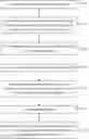
FIG. 1 is a flow chart illustrating a method of manufacturing a flexible display panel according to an embodiment of the present disclosure.
FIGS. 2A-2G are cross-sectional views corresponding to steps S01-S07 applied in FIG. 1.
DETAILED DESCRIPTION OF EMBODIMENTS
To ensure the objects, the technical solutions, and the effects of the disclosure are clearer and more specific, the disclosure will be explained in conjunction with the accompanying drawings in detail further below. It should be understood that the embodiments described herein are merely a part of the embodiments of the present disclosure instead of all of the embodiments and not used to limit the disclosure.
Please refer to FIG. 1, which is a flow chart illustrating a method of manufacturing a flexible display panel according to an embodiment of the present disclosure. Please also refer to FIGS. 2A-2G, which are cross-sectional views corresponding to steps S01-S07 applied in FIG. 1. In FIG. 1, a method of manufacturing the flexible display panel comprises the following steps:
Step S01: forming a first organic layer 21 on a substrate 20 (as shown in FIG. 2A). In some embodiments, the first organic layer 21 is formed through a coating and curing method in step SOL Specifically, the substrate 20 is a glass substrate. Material composition of the first organic layer 21 comprises polyimide. The thickness of the first organic layer 21 is 5 to 15 micrometers.
Step S02: determining a bending area BA on the first organic layer 21 and forming an adhesion layer 22 on a part of the first organic layer 21, located in the bending area BA (as shown in FIG. 2B). In some embodiments, the adhesion layer 22 is formed through a coating method in step S02. Specifically, the adhesion layer 22 comprises at least one material selected from a group consisting of hexamethyldisilazane (HMDS), sorbitol, and dimethyl sulfoxide (DMSO). The thickness of the adhesion layer 22 is 0.01 to 1 micrometer.
Step S03: forming an inorganic layer 23 on the adhesion layer 22 and on the first organic layer 21 (as shown in FIG. 2C). In some embodiments, the inorganic layer 23 is formed through a chemical vapor deposition method in step S03. Specifically, material composition of the inorganic layer 23 comprises SiNx. The thickness of the inorganic layer 23 is 0.1 to 1 micrometer.
Step S04: forming a second organic layer 24 on the inorganic layer 23 (as shown in FIG. 2D). In some embodiments, the second organic layer 24 is formed through a coating and curing method in step S04. Specifically, material composition of the second organic layer 24 comprises polyimide. The thickness of the second organic layer 21 is 5 to 15 micrometers.
Step S05: forming a thin-film transistor layer 25, an organic light-emitting diode layer 26, and an encapsulation layer 27 on the second organic layer 24 in sequence (as shown in FIG. 2E).
Step S06: removing the substrate 20 (as shown in FIG. 2F). In some embodiments, the substrate 20 is stripped through a laser in step S06.
Step S07: removing the part of the first organic layer 21, located in the bending area BA, and the adhesion layer 22 so that a flexible display panel 2 is formed (as shown in FIG. 2G). In some embodiments, the first organic layer 21 is cut through a laser in step S07 in order to remove the part of the first organic layer 21, located in the bending area BA. Furthermore, the adhesion layer 22 peels off due to high temperatures.
Continuing to refer to FIG. 2G, the present disclosure provides a flexible substrate 1 having the bending area BA. The flexible substrate 1 comprises the first organic layer 21, the inorganic layer 23, and the second organic layer 24. The first organic layer 21 has a hollow-out portion 210 in the bending area BA. The inorganic layer 23 is formed above the first organic layer 21, and it has a concave portion 230 and a convex portion 231 which are located in the bending area BA. The concave portion 230 is disposed on a surface of the inorganic layer 23, near the first organic layer 21, and the convex portion 231 is disposed on a surface of the inorganic layer 23, far from the first organic layer 21. The second organic layer 24 is formed above the inorganic layer 23, and it has an embedded portion 240 in the bending area BA. The convex portion 231 of the inorganic layer 23 and the embedded portion 240 are embedded with each other. Furthermore, as shown in FIG. 2G, the flexible display panel 2 provided in the present disclosure comprises the flexible substrate 1, and the thin-film transistor layer 25, the organic light-emitting diode layer 26, and the encapsulation layer 27 which overlap above the flexible substrate 1.
In conclusion, the present disclosure provides a flexible substrate, a flexible display panel, and a manufacturing method mainly by thinning a thickness of a flexible substrate with multilayered structure in order to avoid that metal signal lines in a bending area break due to stresses and to ensure that the display panel can display normally.
It should be understood that the application of the present disclosure is not limited by the foregoing examples. A person of ordinary skill in the art is able to make modifications or changes based on the foregoing description, and all of these modifications and changes are within the scope of the appended claims of the present disclosure.
The industrial applicability of the present disclosure is that, it can avoid that metal signal lines in a bending area break due to stresses and ensure that a display panel can display normally.
Claims
What is claimed is:1. A flexible substrate having a bending area, the flexible substrate comprising:
a first organic layer having a hollow-out portion in the bending area;
an inorganic layer formed above the first organic layer, wherein the inorganic layer has a concave portion and a convex portion which are located in the bending area, wherein the concave portion is disposed on a surface of the inorganic layer, near the first organic layer, and wherein the convex portion is disposed on a surface of the inorganic layer, far from the first organic layer; and
a second organic layer formed above the inorganic layer, wherein the second organic layer has an embedded portion in the bending area, and wherein the embedded portion and the convex portion of the inorganic layer are embedded with each other.
2. The flexible substrate of claim 1, wherein material composition of the first organic layer comprises polyimide.
3. The flexible substrate of claim 1, wherein material composition of the inorganic layer comprises SiNx.
4. The flexible substrate of claim 1, wherein material composition of the second organic layer comprises polyimide.
5. A flexible display panel, comprising a flexible substrate, and a thin-film transistor layer, an organic light-emitting diode layer, and an encapsulation layer which overlap above the flexible substrate, wherein the flexible substrate comprises:
a first organic layer having a hollow-out portion in a bending area;
an inorganic layer formed above the first organic layer, wherein the inorganic layer has a concave portion and a convex portion which are located in the bending area, wherein the concave portion is disposed on a surface of the inorganic layer, near the first organic layer, and wherein the convex portion is disposed on a surface of the inorganic layer, far from the first organic layer; and
a second organic layer formed above the inorganic layer, wherein the second organic layer has an embedded portion in the bending area, and wherein the embedded portion and the convex portion of the inorganic layer are embedded with each other.
6. A method of manufacturing a flexible display panel, comprising:
forming a first organic layer on a substrate;
determining a bending area on the first organic layer and forming an adhesion layer on a part of the first organic layer, located in the bending area;
forming an inorganic layer on the adhesion layer and on the first organic layer;
forming a second organic layer on the inorganic layer;
forming a thin-film transistor layer, an organic light-emitting diode layer, and an encapsulation layer on the second organic layer in sequence;
removing the substrate; and
removing the part of the first organic layer, located in the bending area, and the adhesion layer so that the flexible display panel is formed.
7. The method of claim 6, wherein the step of forming the adhesion layer on a part of the first organic layer, located in the bending area, comprises: forming the adhesion layer through a coating method.
8. The method of claim 6, wherein the step of forming an inorganic layer on the adhesion layer and on the first organic layer comprises: forming the inorganic layer through a chemical vapor deposition method.
9. The method of claim 6, wherein the step of removing the part of the first organic layer, located in the bending area, comprises: cutting the first organic layer through a laser.
10. The method of claim 6, wherein the adhesion layer comprises at least one material selected from a group consisting of hexamethyldisilazane (HMDS), sorbitol, and dimethyl sulfoxide (DMSO).
Images & Drawings included:


Sources:
- United States Patent and Trademark Office - verify current appl. status at the USPTO↗
Similar patent applications:
- » 20210202530
Array substrate, manufacturing method thereof, flexible display panel and display device - » 20170133407
Flexible substrate and manufacturing method thereof, flexible display panel and flexible display device - » 20190157587
Flexible display substrate, manufacturing method thereof, and display panel - » 20210335846
Array substrate and manufacturing method thereof, flexible display panel - » 20160351849
Array substrate and manufacturing method thereof, flexible display panel and display device - » 20190081086
Flexible array substrate and manufacturing method thereof, flexible display panel and display apparatus - » 20210143234
Flexible substrate, manufacturing method thereof, and display panel having the same - » 20190348473
FLEXIBLE SUBSTRATE, MANUFACTURING METHOD THEREOF AND TOUCH DISPLAY PANEL - » 20190305235
Flexible substrate and manufacturing method thereof, manufacturing method of display panel and display device - » 20130213565
FLEXIBLE SUBSTRATE FOR DISPLAY PANEL AND MANUFACTURING METHOD THEREOF
Recent applications in this class:
- » 20230320187 2023-10-05
DISPLAY DEVICE AND METHOD FOR MANUFACTURING THE SAME - » 20230263044 2023-08-17
Method of manufacturing display panel, display panel, and mobile terminal - » 20230217801 2023-07-06
DISPLAY APPARATUS - » 20230217800 2023-07-06
DISPLAY APPARATUS - » 20230217799 2023-07-06
Display Device - » 20230209982 2023-06-29
Display Device - » 20230145495 2023-05-11
DISPLAY DEVICE AND METHOD FOR MANUFACTURING THE SAME - » 20230142422 2023-05-11
Display panel - » 20230130999 2023-04-27
DISPLAY PANEL AND DISPLAY APPARATUS INCLUDING THE SAME - » 20230127915 2023-04-27
Display device and method of providing the same
Recent applications for this Assignee:
- » 20250157409 2025-05-15
GATE DRIVER UNIT AND DISPLAY PANEL - » 20250157389 2025-05-15
PIXEL DRIVING CIRCUIT AND DISPLAY PANEL - » 20250104606 2025-03-27
DISPLAY PANEL AND ELECTRONIC APPARATUS - » 20250087131 2025-03-13
GOA Circuit and Display Panel - » 20240420621 2024-12-19
Gate drive circuits and display panels - » 20240379045 2024-11-14
Display panel and display device - » 20240377861 2024-11-14
FLEXIBLE DISPLAY DEVICE AND SUPPORT ASSEMBLY - » 20240361811 2024-10-31
FOLDABLE DEVICE AND DISPLAY DEVICE - » 20240361810 2024-10-31
DISPLAY DEVICE AND FOLDING DISPLAY MODULE THEREOF - » 20240302866 2024-09-12
Display module and display device