SEMICONDUCTOR PHOTORESIST COMPOSITION AND METHOD OF FORMING PATTERNS USING THE COMPOSITION
US20260118752A1
2026-04-30
19/348,487
2025-10-02
Smart Summary: A special mixture is created for use in making patterns on semiconductors. This mixture includes a metal-based compound, an alcohol that has a double bond, and a liquid to help it spread. The combination helps in forming clear and precise patterns needed for electronic devices. The method involves applying this mixture to a surface and then using light to create the desired designs. Overall, this technology is important for improving the production of electronic components. 🚀 TL;DR
Abstract:
Disclosed are a semiconductor photoresist composition and a method of forming patterns using the same, the semiconductor photoresist composition including an organometallic compound; an alcohol compound including an unsaturated bond; and a solvent.
Inventors:
- Jung-min CHOI 12 🇰🇷 Suwon-si, South Korea
- Jaeyeol BAEK 25 🇰🇷 Suwon-si, South Korea
- Bukeun OH 8 🇰🇷 Suwon-si, South Korea
- Seol Hee LIM 13 🇰🇷 Suwon-si, South Korea
- Miyeon HAN 11 🇰🇷 Suwon-si, South Korea
- Hyejin JANG 7 🇰🇷 Suwon-si, South Korea
- Jonghyuk JEON 2 🇰🇷 Suwon-si, South Korea
- Seunghwan BYUN 2 🇰🇷 Suwon-si, South Korea
- Sanghoon SHIN 2 🇰🇷 Suwon-si, South Korea
Applicant:
Interested in similar patents?
Get notified when new applications in this technology area are published.
Classification:
G03F7/0042 » CPC main
Photomechanical, e.g. photolithographic, production of textured or patterned surfaces, e.g. printing surfaces; Materials therefor, e.g. comprising photoresists; Apparatus specially adapted therefor; Photosensitive materials with inorganic or organometallic light-sensitive compounds not otherwise provided for, e.g. inorganic resists
G03F7/0045 » CPC further
Photomechanical, e.g. photolithographic, production of textured or patterned surfaces, e.g. printing surfaces; Materials therefor, e.g. comprising photoresists; Apparatus specially adapted therefor; Photosensitive materials with organic non-macromolecular light-sensitive compounds not otherwise provided for, e.g. dissolution inhibitors
G03F7/2004 » CPC further
Photomechanical, e.g. photolithographic, production of textured or patterned surfaces, e.g. printing surfaces; Materials therefor, e.g. comprising photoresists; Apparatus specially adapted therefor; Exposure; Apparatus therefor with visible light or UV light, through an original having an opaque pattern on a transparent support, e.g. film printing, projection printing; by reflection of visible or UV light from an original such as a printed image characterised by the use of a particular light source, e.g. fluorescent lamps or deep UV light
G03F7/004 IPC
Photomechanical, e.g. photolithographic, production of textured or patterned surfaces, e.g. printing surfaces; Materials therefor, e.g. comprising photoresists; Apparatus specially adapted therefor Photosensitive materials
G03F7/20 IPC
Photomechanical, e.g. photolithographic, production of textured or patterned surfaces, e.g. printing surfaces; Materials therefor, e.g. comprising photoresists; Apparatus specially adapted therefor Exposure; Apparatus therefor
H01L21/027 IPC
Processes or apparatus adapted for the manufacture or treatment of semiconductor or solid state devices or of parts thereof; Manufacture or treatment of semiconductor devices or of parts thereof Making masks on semiconductor bodies for further photolithographic processing not provided for in group or
Description
CROSS-REFERENCE TO RELATED APPLICATION
The present application claims priority to and the benefit of Korean Patent Application No. 10-2024-0152904, filed on Oct. 31, 2024, in the Korean Intellectual Property Office, the entire content of which is hereby incorporated by reference.
BACKGROUND
1. Field
Embodiments of this disclosure relate to a semiconductor photoresist composition and a method of forming patterns using the same.
2. Description of the Related Art
EUV (extreme ultraviolet) lithography is paid attention to as one technology for manufacturing a next generation semiconductor device. The EUV lithography is a pattern-forming technology using an EUV ray having a wavelength of 13.5 nm as an exposure light source. According to the EUV lithography, an extremely fine pattern (e.g., less than or equal to 20 nm) may be formed in an exposure process during a manufacture of a semiconductor device.
The extreme ultraviolet (EUV) lithography is realized through development of compatible photoresists which can be performed at a spatial resolution of less than or equal to 16 nm. Currently, efforts to satisfy insufficient specifications of traditional chemically amplified (CA) photoresists such as a resolution, a photospeed, and feature roughness (which may also be referred to as a line edge roughness or LER) for the next generation device are being made.
An intrinsic image blurring due to an acid catalyzed reaction in these polymer-type photoresists limits a resolution in small feature sizes, which has been present in electron beam (e-beam) lithography for a long time. The chemically amplified (CA) photoresists are designed for high sensitivity, but because their elemental makeups reduce light absorbance of the photoresists at a wavelength of 13.5 nm and thus decrease their sensitivity, the chemically amplified (CA) photoresists may partially have more difficulties under an EUV exposure.
The CA photoresists may have difficulties in the small feature sizes due to roughness issues, and line edge roughness (LER) of the CA photoresists experimentally turns out to be increased, as a photospeed is decreased partially due to an essence of acid catalyst processes. Accordingly, a high-performance photoresist is desired or required in a semiconductor industry because of these defects and problems of the CA photoresists.
In order to overcome the aforementioned drawbacks of the chemically amplified (CA) organic photosensitive composition, an inorganic photosensitive composition has been researched. The inorganic photosensitive composition is mainly used for negative tone patterning having resistance against removal by a developer composition due to chemical modification through nonchemical amplification mechanism. The inorganic composition contains an inorganic element having a higher EUV absorption rate than hydrocarbon and thus may secure sensitivity through the nonchemical amplification mechanism and is less sensitive about a stochastic effect and thus has low line edge roughness and a small number of defects.
Inorganic photoresists based on peroxopolyacids of tungsten mixed with tungsten, niobium, titanium, and/or tantalum have been reported as radiation sensitive materials for patterning.
These materials are effective for patterning large pitches for bilayer configuration as far ultraviolet (deep UV), X-ray, and electron beam sources. More recently, if (e.g., when) cationic hafnium metal oxide sulfate (HfSOx) materials along with a peroxo complexing agent has been used to image a 15 nm half-pitch (HP) through projection EUV exposure, impressive performance has been obtained. This system exhibits the highest performance of a non-CA photoresist and has a practicable photospeed near suitable for an EUV photoresist. However, the hafnium metal oxide sulfate material having the peroxo complexing agent has a few practical drawbacks. First, these materials are coated in a mixture of corrosive sulfuric acid/hydrogen peroxide and have insufficient shelf-life stability. Second, a structural change thereof for performance improvement as a composite mixture is not easy. Third, development should be performed in a TMAH (tetramethylammonium hydroxide) solution at an extremely high concentration of 25 wt % and/or the like.
Recently, active research has been conducted into molecules including tin that have excellent absorption of extreme ultraviolet rays. As for an organotin polymer among them, alkyl ligands are dissociated by light absorption and/or secondary electrons produced thereby, and are crosslinked with adjacent chains through oxo bonds and thus enable the negative tone patterning which may not be removed by an organic developer. This organotin polymer exhibits greatly improved sensitivity as well as maintains a resolution and line edge roughness, but the patterning characteristics should be additionally improved for commercial availability.
SUMMARY
Some example embodiments of the present disclosure provide a semiconductor photoresist composition having improved sensitivity and LER characteristics.
Some example embodiments provide a method of forming patterns using the semiconductor photoresist composition.
A semiconductor photoresist composition according to some example embodiments includes an organometallic compound; an alcohol compound including an unsaturated bond; and a solvent.
A method of forming patterns according to some example embodiments includes providing or forming an etching-objective layer on a substrate, coating the semiconductor photoresist composition on the etching-objective layer to form a photoresist film, patterning the photoresist film to form a photoresist pattern, and etching the etching-objective layer using the photoresist pattern as an etching mask.
The semiconductor photoresist composition according to some example embodiments can provide a photoresist pattern having improved sensitivity and LER characteristics.
BRIEF DESCRIPTION OF THE DRAWINGS
The accompanying drawings, together with the specification, illustrate embodiments of the subject matter of the present disclosure, and, together with the description, serve to explain principles of embodiments of the subject matter of the present disclosure.
FIGS. 1A-1E are cross-sectional views that illustrate a method of forming patterns using a semiconductor photoresist composition according to some example embodiments.
DETAILED DESCRIPTION
Hereinafter, referring to the drawings, embodiments are described in more detail. In the following description of the present disclosure, well-known functions or constructions will not be described in order to clarify the subject matter of the present disclosure.
In order to clearly illustrate the subject matter of the present disclosure, certain description and relationships are omitted, and throughout the disclosure, the same or similar configuration elements are designated by the same reference numerals. Also, because the size and thickness of each configuration shown in the drawings may be arbitrarily shown for better understanding and ease of description, the present disclosure is not necessarily limited thereto.
In the drawings, the thickness of layers, films, panels, regions, and/or the like, may be exaggerated for clarity. In the drawings, the thickness of a part of layers or regions, and/or the like, may be exaggerated for convenience of explanation. It will be understood that if (e.g., when) an element such as a layer, film, region, or substrate is referred to as being “on” another element, it can be directly on the other element or intervening elements may also be present.
As used herein, the term “substituted” refers to replacement of a hydrogen atom by deuterium, a halogen, a hydroxy group, a carboxyl group, a thiol group, a cyano group, a nitro group, —NRR′ (wherein, R and R′ are each independently hydrogen, a substituted or unsubstituted C1 to C30 saturated or unsaturated aliphatic hydrocarbon group, a substituted or unsubstituted C3 to C30 saturated or unsaturated alicyclic hydrocarbon group, or a substituted or unsubstituted C6 to C30 aromatic hydrocarbon group), —SiRR′R″ (wherein, R, R′, and R″ are each independently hydrogen, a substituted or unsubstituted C1 to C30 saturated or unsaturated aliphatic hydrocarbon group, a substituted or unsubstituted C3 to C30 saturated or unsaturated alicyclic hydrocarbon group, or a substituted or unsubstituted C6 to C30 aromatic hydrocarbon group), a C1 to C30 alkyl group, a C1 to C10 haloalkyl group, a C1 to C10 alkylsilyl group, a C3 to C30 cycloalkyl group, a C6 to C30 aryl group, a C1 to C20 alkoxy group, a C1 to C20 sulfide group, or a combination thereof. The term “unsubstituted” refers to non-replacement of a hydrogen atom by another substituent and remaining of the hydrogen atom.
As used herein, if (e.g., when) a definition is not otherwise provided, the term “alkyl group” refers to a linear or branched aliphatic hydrocarbon group. The alkyl group may be “saturated alkyl group” without any double bond or triple bond.
The alkyl group may be a C1 to C8 alkyl group. For example, the alkyl group may be a C1 to C7 alkyl group, a C1 to C6 alkyl group, or a C1 to C5 alkyl group. For example, the C1 to C5 alkyl group may be a methyl group, an ethyl group, a propyl group, an isopropyl group, an n-butyl group, an isobutyl group, a sec-butyl group, a tert-butyl group, or a 2,2-dimethylpropyl group.
As used herein, if (e.g., when) a definition is not otherwise provided, the term “cycloalkyl group” refers to a monovalent cyclic aliphatic hydrocarbon group.
The cycloalkyl group may be a C3 to C8 cycloalkyl group, for example, a C3 to C7 cycloalkyl group, or a C3 to C6 cycloalkyl group. For example, the cycloalkyl group may be a cyclopropyl group, a cyclobutyl group, a cyclopentyl group, or a cyclohexyl group, but is not limited thereto.
As used herein, the term “aryl group” refers to a substituent in which all atoms in the cyclic substituent have a p-orbital and these p-orbitals are conjugated and may include a monocyclic or fused ring polycyclic functional group (e.g., rings sharing adjacent pairs of carbon atoms).
As used herein, the term “unsaturated bond” means a double bond or a triple bond, and the number of unsaturated bonds contained in one molecule is not particularly limited. For example, it may be ethylene, propylene, butene, pentene, hexene, and/or acetylene.
Hereinafter, a semiconductor photoresist composition according to some example embodiments is described.
A semiconductor photoresist composition according to some example embodiments includes an organometallic compound, an alcohol compound including an unsaturated bond, and a solvent.
The total composition, by virtue of the alcohol compound including an unsaturated bond included in the semiconductor photoresist composition according to embodiments of the present disclosure, not only promotes intermolecular bonding after exposure, but also improves sensitivity by making the intermolecular bonding thus formed more smoothly by heat treatment after exposure.
In embodiments, the unshared electron pair of alcohol increases the adsorption to the substrate, which can improve surface roughness and LER characteristics.
For example, the alcohol compound including the unsaturated bond may be represented by any one selected from Chemical Formula 1 to Chemical Formula 4.
In Chemical Formula 1 to Chemical Formula 4,
-
- R1 to R12 are each independently hydrogen, a substituted or unsubstituted C1 to C20 alkyl group, a substituted or unsubstituted C2 to C20 alkenyl group, a substituted or unsubstituted C2 to C20 alkynyl group, a substituted or unsubstituted C1 to C20 alkylene group, a substituted or unsubstituted C2 to C20 alkenylene group, a substituted or unsubstituted C2 to C20 alkynylene group, or a combination thereof,
- L1 and L2 are each independently a substituted or unsubstituted C1 to C10 alkylene group, a substituted or unsubstituted C2 to C20 alkenylene group, a substituted or unsubstituted C2 to C20 alkynylene group, or a combination thereof,
- m1 to m12 are each independently an integer of 0 or 1,
- m1+m2+m3+m4 and m5+m6+m7+m8 are each independently one of
- integers from 1 to 4, and
- m9+m10 and m11+m12 are each independently an integer of 1 or 2.
As an example, the alcohol compound including the unsaturated bond may include 1 to 4-OH groups, for example, 1 to 3-OH groups, or, for example, 1 or 2-OH groups.
In some example embodiments, the m1+m2+m3+m4 and m5+m6+m7+m8 may each independently be an integer from 1 to 3, for example, an integer of 1 or 2.
For example, if (e.g., when) R1 to R12 are terminal substituents, they may be substituted or unsubstituted C1 to C20 alkyl groups.
For example, if (e.g., when) R1 to R12 are linked to an —OH group, they may be substituted or unsubstituted C1 to C20 alkylene groups.
As an example, if (e.g., when) R1 to R12 are terminal substituents, they may be substituted or unsubstituted C1 to C10 alkyl groups.
As an example, if (e.g., when) R1 to R12 are linked to an —OH group, they may be substituted or unsubstituted C1 to C10 alkylene groups.
For example, if (e.g., when) R1 to R12 are terminal substituents, they may be a substituted or unsubstituted methyl group, a substituted or unsubstituted ethyl group, a substituted or unsubstituted propyl group, or a substituted or unsubstituted butyl group.
For example, if (e.g., when) R1 to R12 are linked to an —OH group, they may be a substituted or unsubstituted methylene group, a substituted or unsubstituted ethylene group, a substituted or unsubstituted propylene group, or a substituted or unsubstituted butylene group.
For example, L1 and L2 may each independently be a substituted or unsubstituted C1 to C5 alkylene group.
As an example, L1 and L2 may each independently be a substituted or unsubstituted methylene group, a substituted or unsubstituted ethylene group, or a substituted or unsubstituted propylene group.
For example, the alcohol compound including the unsaturated bond may be selected from the compounds listed in Group 1.
The alcohol compound including the unsaturated bond may be included in an amount of about 0.001 to about 5 wt % based on 100 wt % of the semiconductor photoresist composition.
For example, the alcohol compound including the unsaturated bond may be included in an amount of about 0.005 to about 5 wt %, about 0.01 to about 5 wt %, or about 0.03 to about 5 wt % based on 100 wt % of the semiconductor photoresist composition.
The organometallic compound may be included in an amount of about 0.5 wt % to about 30 wt % based on 100 wt % of the semiconductor photoresist composition.
The semiconductor photoresist composition according to some example embodiments can improve the sensitivity of the photoresist by including the alcohol compound including the unsaturated bond within the above amount ranges.
The organometallic compound may be an organotin compound including at least one selected from an organic oxy group and an organic carbonyloxy group.
For example, the organometallic compound may be represented by Chemical Formula 5.
In Chemical Formula 5,
-
- R13 is selected from a substituted or unsubstituted C1 to C20 alkyl group, a substituted or unsubstituted C3 to C20 cycloalkyl group, a substituted or unsubstituted C2 to C20 alkenyl group, a substituted or unsubstituted C2 to C20 alkynyl group, a substituted or unsubstituted C6 to C30 aryl group, and a substituted or unsubstituted C7 to C30 arylalkyl group,
- R14 to R16 are each independently a substituted or unsubstituted C1 to C20 alkyl group, a substituted or unsubstituted C3 to C20 cycloalkyl group, a substituted or unsubstituted C2 to C20 alkenyl group, a substituted or unsubstituted C2 to C20 alkynyl group, a substituted or unsubstituted C6 to C30 aryl group, a substituted or unsubstituted C7 to C30 arylalkyl group, alkoxy and/or aryloxy group (—ORb, wherein Rb is a substituted or unsubstituted C1 to C20 alkyl group, a substituted or unsubstituted C3 to C20 cycloalkyl group, a substituted or unsubstituted C6 to C30 aryl group, or a combination thereof), a carboxyl group (—O(CO)Rc, wherein Rc is hydrogen, a substituted or unsubstituted C1 to C20 alkyl group, a substituted or unsubstituted C3 to C20 cycloalkyl group, a substituted or unsubstituted C2 to C20 alkenyl group, a substituted or unsubstituted C2 to C20 alkynyl group, a substituted or unsubstituted C6 to C30 aryl group, or a combination thereof), —NRdRe, wherein Rd and Re are each independently hydrogen, a substituted or unsubstituted C1 to C20 alkyl group, a substituted or unsubstituted C3 to C20 cycloalkyl group, a substituted or unsubstituted C2 to C20 alkenyl group, a substituted or unsubstituted C2 to C20 alkynyl group, a substituted or unsubstituted C6 to C30 aryl group, or a combination thereof, —NRf(CORg), wherein Rf and Rg are each independently hydrogen, a substituted or unsubstituted C1 to C20 alkyl group, a substituted or unsubstituted C3 to C20 cycloalkyl group, a substituted or unsubstituted C2 to C20 alkenyl group, a substituted or unsubstituted C2 to C20 alkynyl group, a substituted or unsubstituted C6 to C30 aryl group, or a combination thereof, —NRhC(NRi)Rj, wherein Rh, Ri, and Rj are each independently hydrogen, a substituted or unsubstituted C1 to C20 alkyl group, a substituted or unsubstituted C3 to C20 cycloalkyl group, a substituted or unsubstituted C2 to C20 alkenyl group, a substituted or unsubstituted C2 to C20 alkynyl group, a substituted or unsubstituted C6 to C30 aryl group, or a combination thereof, —SRk, wherein Rk is a substituted or unsubstituted C1 to C20 alkyl group, a substituted or unsubstituted C3 to C20 cycloalkyl group, a substituted or unsubstituted C2 to C20 alkenyl group, a substituted or unsubstituted C2 to C20 alkynyl group, a substituted or unsubstituted C6 to C30 aryl group, or a combination thereof, and/or —S(CO)Rl, wherein Rl is hydrogen, a substituted or unsubstituted C1 to C20 alkyl group, a substituted or unsubstituted C3 to C20 cycloalkyl group, a substituted or unsubstituted C2 to C20 alkenyl group, a substituted or unsubstituted C2 to C20 alkynyl group, a substituted or unsubstituted C6 to C30 aryl group, or a combination thereof, and
- at least one selected from R14 to R16 is selected from alkoxy and/or aryloxy group (—ORb, wherein Rb is a substituted or unsubstituted C1 to C20 alkyl group, a substituted or unsubstituted C3 to C20 cycloalkyl group, a substituted or unsubstituted C6 to C30 aryl group, or a combination thereof), a carboxyl group (—O(CO)Rc, wherein Rc is hydrogen, a substituted or unsubstituted C1 to C20 alkyl group, a substituted or unsubstituted C3 to C20 cycloalkyl group, a substituted or unsubstituted C2 to C20 alkenyl group, a substituted or unsubstituted C2 to C20 alkynyl group, a substituted or unsubstituted C6 to C30 aryl group, or a combination thereof), —NRdRe, wherein Rd and Re are each independently hydrogen, a substituted or unsubstituted C1 to C20 alkyl group, a substituted or unsubstituted C3 to C20 cycloalkyl group, a substituted or unsubstituted C2 to C20 alkenyl group, a substituted or unsubstituted C2 to C20 alkynyl group, a substituted or unsubstituted C6 to C30 aryl group, or a combination thereof, —NRf(CORg), wherein Rf and Rg are each independently hydrogen, a substituted or unsubstituted C1 to C20 alkyl group, a substituted or unsubstituted C3 to C20 cycloalkyl group, a substituted or unsubstituted C2 to C20 alkenyl group, a substituted or unsubstituted C2 to C20 alkynyl group, a substituted or unsubstituted C6 to C30 aryl group, or a combination thereof, —NRgC(NRh)Ri, wherein Rh, Ri and Rj are each independently hydrogen, a substituted or unsubstituted C1 to C20 alkyl group, a substituted or unsubstituted C3 to C20 cycloalkyl group, a substituted or unsubstituted C2 to C20 alkenyl group, a substituted or unsubstituted C2 to C20 alkynyl group, a substituted or unsubstituted C6 to C30 aryl group, or a combination thereof, —SRk, wherein Rk is a substituted or unsubstituted C1 to C20 alkyl group, a substituted or unsubstituted C3 to C20 cycloalkyl group, a substituted or unsubstituted C2 to C20 alkenyl group, a substituted or unsubstituted C2 to C20 alkynyl group, a substituted or unsubstituted C6 to C30 aryl group, or a combination thereof, and/or —S(CO)Rl, Rl is hydrogen, a substituted or unsubstituted C1 to C20 alkyl group, a substituted or unsubstituted C3 to C20 cycloalkyl group, a substituted or unsubstituted C2 to C20 alkenyl group, a substituted or unsubstituted C2 to C20 alkynyl group, a substituted or unsubstituted C6 to C30 aryl group, or a combination thereof.
At least one selected from R14 to R16 may be selected from alkoxy and/or aryloxy group (—ORb, wherein Rb is a substituted or unsubstituted C1 to C20 alkyl group, a substituted or unsubstituted C3 to C20 cycloalkyl group, a substituted or unsubstituted C6 to C30 aryl group, or a combination thereof), and/or carboxyl group (—O(CO)Rc, wherein Rc is hydrogen, a substituted or unsubstituted C1 to C20 alkyl group, a substituted or unsubstituted C3 to C20 cycloalkyl group, a substituted or unsubstituted C2 to C20 alkenyl group, a substituted or unsubstituted C2 to C20 alkynyl group, a substituted or unsubstituted C6 to C30 aryl group, or a combination thereof).
In embodiments, because the compound represented by Chemical Formula 5 includes —ORb or —OC(═O)Rc as a ligand, a pattern formed using a semiconductor photoresist composition including the compound may exhibit excellent limit resolution (e.g., excellent line resolution).
In embodiments, the ligand of —ORb or —OC(═O)Rc may determine the solubility of the compound represented by Chemical Formula 5 in a solvent.
-
- R13 may be a substituted or unsubstituted C1 to C8 alkyl group, a substituted or unsubstituted C3 to C8 cycloalkyl group, a substituted or unsubstituted C2 to C8 aliphatic unsaturated organic group including one or more double bonds or triple bonds, a substituted or unsubstituted C6 to C20 aryl group, a substituted or unsubstituted C4 to C20 heteroaryl group, a carbonyl group, an ethoxy group, a propoxy group, or a combination thereof,
- Rb may be a substituted or unsubstituted C1 to C8 alkyl group, a substituted or unsubstituted C3 to C8 cycloalkyl group, a substituted or unsubstituted C2 to C8 alkenyl group, a substituted or unsubstituted C2 to C8 alkynyl group, a substituted or unsubstituted C6 to C20 aryl group, or a combination thereof, and
- Rc may be hydrogen, a substituted or unsubstituted C1 to C8 alkyl group, a substituted or unsubstituted C3 to C8 cycloalkyl group, a substituted or unsubstituted C2 to C8 alkenyl group, a substituted or unsubstituted C2 to C8 alkynyl group, a substituted or unsubstituted C6 to C20 aryl group, or a combination thereof.
- R13 may be a methyl group, an ethyl group, a propyl group, a butyl group, an isopropyl group, a tert-butyl group, a 2,2-dimethylpropyl group, a cyclopropyl group, a cyclobutyl group, a cyclopentyl group, a cyclohexyl group, an ethenyl group, a propenyl group, a butenyl group, an ethynyl group, a propynyl group, a butynyl group, a phenyl group, a tolyl group, a xylene group, a benzyl group, a formyl group, an acetyl group, a propanoyl group, a butanoyl group, a pentanoyl group, an ethoxy group, a propoxy group, or a combination thereof,
- Rb may be an ethyl group, a propyl group, a butyl group, an isopropyl group, a tert-butyl group, a 2,2-dimethylpropyl group, a cyclopropyl group, a cyclobutyl group, a cyclopentyl group, a cyclohexyl group, an ethenyl group, a propenyl group, a butenyl group, an ethynyl group, a propynyl group, a butynyl group, a phenyl group, a tolyl group, a xylene group, a benzyl group, or a combination thereof, and
- Rc may be hydrogen, an ethyl group, a propyl group, a butyl group, an isopropyl group, a tert-butyl group, a 2,2-dimethylpropyl group, a cyclopropyl group, a cyclobutyl group, a cyclopentyl group, a cyclohexyl group, an ethenyl group, a propenyl group, a butenyl group, an ethynyl group, a propynyl group, a butynyl group, a phenyl group, a tolyl group, a xylene group, a benzyl group, or a combination thereof.
In embodiments, the organometallic compound may be represented by Chemical Formula 6 or Chemical Formula 7.
In Chemical Formula 6,
-
- R17 is a C1 to C31 hydrocarbyl group, 0<z≤2, and 0<(z+x)≤4;
-
- wherein, in Chemical Formula 7,
- R18 is a substituted or unsubstituted C1 to C20 alkyl group, a substituted or unsubstituted C3 to C20 cycloalkyl group, a substituted or unsubstituted C2 to C20 aliphatic unsaturated organic group including one or more double bonds or triple bonds, a substituted or unsubstituted C6 to C30 aryl group, a substituted or unsubstituted C4 to C30 heteroaryl group, a carbonyl group, ethylene oxide group, propylene oxide group, or a combination thereof,
- X is sulfur(S), selenium (Se), or tellurium (Te),
- Y is —ORm or —OC(═O)Rn,
- wherein Rm is a substituted or unsubstituted C1 to C20 alkyl group, a substituted or unsubstituted C3 to C20 cycloalkyl group, a substituted or unsubstituted C2 to C20 alkenyl group, a substituted or unsubstituted C2 to C20 alkynyl group, a substituted or unsubstituted C6 to C30 aryl group, or a combination thereof, and
- Rn is hydrogen, a substituted or unsubstituted C1 to C20 alkyl group, a substituted or unsubstituted C3 to C20 cycloalkyl group, a substituted or unsubstituted C2 to C20 alkenyl group, a substituted or unsubstituted C2 to C20 alkynyl group, a substituted or unsubstituted C6 to C30 aryl group, or a combination thereof, and
- a, b, c, and d are each independently an integer of 1 to 20.
The solvent included in the semiconductor photoresist composition according to some example embodiments may be an organic solvent, and may be for example aromatic compounds (e.g., xylene, toluene, and/or the like), alcohols (e.g., 4-methyl-2-pentenol, 4-methyl-2-propanol, 1-butanol, methanol, isopropyl alcohol, 1-propanol, and/or the like), ethers (e.g., anisole, tetrahydrofuran, and/or the like), esters (n-butyl acetate, propylene glycol monomethyl ether acetate, ethyl acetate, ethyl lactate, and/or the like), ketones (e.g., methyl ethyl ketone, 2-heptanone, and/or the like), or a mixture thereof, but is not limited thereto.
The semiconductor photoresist composition according to some example embodiments may further include a resin in addition to the aforementioned organometallic compound, alcohol compound including the unsaturated bond and solvent.
The resin may be a phenol-based resin including at least one aromatic moiety listed in Group 2.
The resin may have a weight average molecular weight of about 500 to about 20,000.
The resin may be included in an amount of about 0.1 wt % to about 50 wt % based on a total amount of the semiconductor photoresist composition.
If the resin is included in the above amount range, it may have excellent etch resistance and heat resistance.
In embodiments, the semiconductor photoresist composition may be composed of the aforementioned organometallic compound, alcohol compound including the unsaturated bond, solvent, and resin.
The semiconductor photoresist composition according to the aforementioned embodiments may further include additives as needed. Examples of the additives may be a surfactant, a crosslinking agent, a leveling agent, an organic acid, a quencher, or a combination thereof.
The surfactant may include for example an alkyl benzene sulfonate salt, an alkyl pyridinium salt, polyethylene glycol, a quaternary ammonium salt, or a combination thereof, but is not limited thereto.
The crosslinking agent may be for example a melamine-based crosslinking agent, a substituted urea-based crosslinking agent, an acryl-based crosslinking agent, an epoxy-based crosslinking agent, and/or a polymer-based crosslinking agent, but is not limited thereto. It may be a crosslinking agent having at least two crosslinking forming substituents, for example, a compound such as methoxymethylated glycoluril, butoxymethylated glycoluril, methoxymethylated melamine, butoxymethylated melamine, methoxymethylated benzoguanamine, butoxymethylated benzoguanamine, 4-hydroxybutyl acrylate, acrylic acid, urethane acrylate, acryl methacrylate, 1,4-butanediol diglycidyl ether, glycidol, diglycidyl 1,2-cyclohexane dicarboxylate, trimethylpropane triglycidyl ether, 1,3-bis(glycidoxypropyl)tetramethyldisiloxane, methoxymethylated urea, butoxymethylated urea, methoxymethylated thiourea, and/or the like.
The leveling agent may be used to improve coating flatness during printing and may be any suitable leveling agent generally used in the art.
The organic acid may include p-toluenesulfonic acid, benzenesulfonic acid, p-dodecylbenzenesulfonic acid, 1,4-naphthalenedisulfonic acid, methanesulfonic acid, a fluorinated sulfonium salt, malonic acid, citric acid, propionic acid, methacrylic acid, oxalic acid, lactic acid, glycolic acid, succinic acid, or a combination thereof, but is not limited thereto.
The quencher may be diphenyl (p-tolyl) amine, methyl diphenyl amine, triphenyl amine, phenylenediamine, naphthylamine, diaminonaphthalene, or a combination thereof.
Each use amount of the additives may be controlled depending on suitable or desired properties.
In embodiments, the semiconductor photoresist composition may further include a silane coupling agent as an adherence enhancer in order to improve a close-contacting force with the substrate (e.g., in order to improve adherence of the semiconductor photoresist composition to the substrate). The silane coupling agent may be for example a silane compound including a carbon-carbon unsaturated bond such as vinyltrimethoxysilane, vinyl triethoxysilane, vinyl trichlorosilane, vinyl tris(β-methoxyethoxy) silane; and/or 3-methacryloxypropyltrimethoxysilane, 3-acryloxypropyltrimethoxysilane, p-styryl trimethoxysilane, 3-methacryloxypropylmethyldimethoxysilane, 3-methacryloxypropylmethyl diethoxysilane; trimethoxy [3-(phenylamino)propyl]silane, and/or the like, but is not limited thereto.
The semiconductor photoresist composition may be formed into a pattern having a high aspect ratio without (or substantially without) a collapse. Accordingly, in order to form a fine pattern having a width of, for example, about 5 nm to about 100 nm, for example, about 5 nm to about 80 nm, for example, about 5 nm to about 70 nm, for example, about 5 nm to about 50 nm, for example, about 5 nm to about 40 nm, for example, about 5 nm to about 30 nm, or for example, about 5 nm to about 20 nm, the semiconductor photoresist composition may be used for a photoresist process using light having a wavelength in a range from about 5 nm to about 150 nm, for example, about 5 nm to about 100 nm, about 5 nm to about 80 nm, about 5 nm to about 50 nm, about 5 nm to about 30 nm, or about 5 nm to about 20 nm. Accordingly, the semiconductor photoresist composition according to some example embodiments may be used to realize extreme ultraviolet lithography using an EUV light source having a wavelength of about 13.5 nm.
According to some example embodiments, a method of forming patterns using the aforementioned semiconductor photoresist composition is provided. For example, the manufactured pattern may be a photoresist pattern.
The method of forming patterns according to some example embodiments includes providing or forming an etching-objective layer on a substrate, coating the semiconductor photoresist composition on the etching-objective layer to form a photoresist film, patterning the photoresist film to form a photoresist pattern, and etching the etching-objective layer using the photoresist pattern as an etching mask.
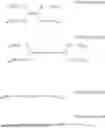
Hereinafter, a method of forming patterns using the semiconductor photoresist composition is described referring to FIGS. 1A-1E. FIGS. 1A-1E are cross-sectional views that illustrate a method of forming patterns using a semiconductor photoresist composition according to some example embodiments.
Referring to FIG. 1A, an object to etch is prepared. The object to etch may be a thin film 102 formed on a semiconductor substrate 100. Hereinafter, the object to etch is limited to the thin film 102, but the present disclosure is not limited thereto. A surface of the thin film 102 is washed to remove impurities and/or the like remaining thereon. The thin film 102 may be for example a silicon nitride layer, a polysilicon layer, and/or a silicon oxide layer.
Subsequently, the resist underlayer composition to form a resist underlayer 104 is spin-coated on the surface of the washed thin film 102. However, the embodiments are not limited thereto, and various suitable coating methods, for example a spray coating, a dip coating, a knife edge coating, a printing method, for example an inkjet printing and a screen printing, and/or the like may be used.
The coating process of the resist underlayer may be omitted, and hereinafter, a process including a coating of the resist underlayer is described.
Then, the coated composition is dried and baked to form a resist underlayer 104 on the thin film 102. The baking may be performed at about 100° C. to about 500° C., for example, about 100° C. to about 300° C.
The resist underlayer 104 is between the substrate 100 and a photoresist film 106 and thus may prevent or reduce non-uniformity and pattern formability of a photoresist line width if (e.g., when) a ray reflected from on the interface between the substrate 100 and the photoresist film 106 and/or a hardmask between layers is scattered into an unintended photoresist region.
Referring to FIG. 1B, the photoresist film 106 is formed by coating the semiconductor photoresist composition on the resist underlayer 104. The photoresist film 106 is obtained by coating the aforementioned semiconductor photoresist composition on the thin film 102 formed on the substrate 100 and then, curing it through a heat treatment.
In embodiments, the formation of a pattern by using the semiconductor photoresist composition may include coating the semiconductor photoresist composition on the substrate 100 having the thin film 102 through spin coating, slit coating, inkjet printing, and/or the like and then, drying it to form the photoresist film 106.
The semiconductor photoresist composition has already been illustrated in detail herein and redundant description thereof may not be repeated herein.
Subsequently, a substrate 100 having the photoresist film 106 is subjected to a first baking process. The first baking process may be performed at about 80° C. to about 120° C.
Referring to FIG. 1C, the photoresist film 106 may be selectively exposed using a patterned mask 110.
For example, the exposure may use an activation radiation with light having a high energy wavelength light such as EUV (extreme ultraviolet; a wavelength of about 13.5 nm), an E-Beam (an electron beam), and/or the like as well as light with a shorter wavelength such as an i-line (a wavelength of about 365 nm), a KrF excimer laser (a wavelength of about 248 nm), an ArF excimer laser (a wavelength of about 193 nm), and/or the like.
In embodiments, light for the exposure according to some example embodiments may be light having a wavelength in a range from about 5 nm to about 150 nm and a high energy wavelength, for example, EUV (extreme ultraviolet; a wavelength of 13.5 nm), an E-Beam (an electron beam), and/or the like.
The exposed region 106b of the photoresist film 106 has a different solubility from the unexposed region 106a of the photoresist film 106 by due to formation of a polymer by a crosslinking reaction such as condensation (e.g., a condensation reaction) between organometallic compounds.
Subsequently, the substrate 100 is subjected to a second baking process. The second baking process may be performed at a temperature of about 90° C. to about 200° C. The exposed region 106b of the photoresist film 106 becomes easily indissoluble with respect to a developer due to the second baking process.
In FIG. 1D, the unexposed region 106a of the photoresist film is dissolved and removed using the developer to form a photoresist pattern 108. For example, the unexposed region 106a of the photoresist film is dissolved and removed by using an organic solvent such as 2-heptanone and/or the like to complete the photoresist pattern 108 corresponding to the negative tone image.
As described above, a developer used in a method of forming patterns according to some example embodiments may be an organic solvent. The organic solvent used in the method of forming patterns according to some example embodiments may be for example ketones such as methylethylketone, acetone, cyclohexanone, 2-heptanone, and/or the like, alcohols such as 4-methyl-2-propanol, 1-butanol, isopropanol, 1-propanol, methanol, and/or the like, esters such as propylene glycol monomethyl ether acetate, ethyl acetate, ethyl lactate, n-butyl acetate, butyrolactone, and/or the like, aromatic compounds such as benzene, xylene, toluene, and/or the like, or a combination thereof.
However, the photoresist pattern according to some example embodiments is not necessarily limited to the negative tone image but may be formed to have a positive tone image. In embodiments, a developer used for forming the positive tone image may be a quaternary ammonium hydroxide composition such as tetraethylammonium hydroxide, tetrapropylammonium hydroxide, tetrabutylammonium hydroxide, or a combination thereof.
As described above, exposure to light having a high energy such as EUV (extreme ultraViolet; a wavelength of 13.5 nm), an E-Beam (an electron beam), and/or the like as well as light having a short wavelength such as i-line (wavelength of about 365 nm), KrF excimer laser (wavelength of about 248 nm), ArF excimer laser (wavelength of about 193 nm), and/or the like may provide a photoresist pattern 108 having a width of a thickness of about 5 nm to about 100 nm. For example, the photoresist pattern 108 may have a width of a thickness of about 5 nm to about 90 nm, about 5 nm to about 80 nm, about 5 nm to about 70 nm, about 5 nm to about 60 nm, about 5 nm to about 50 nm, about 5 nm to about 40 nm, about 5 nm to about 30 nm, or about 5 nm to about 20 nm.
In embodiments, the photoresist pattern 108 may have a pitch of having a half-pitch of less than or equal to about 50 nm, for example less than or equal to about 40 nm, for example less than or equal to about 30 nm, for example less than or equal to about 20 nm, or for example less than or equal to about 15 nm, and a line width roughness of less than or equal to about 10 nm, less than or equal to about 5 nm, less than or equal to about 3 nm, or less than or equal to about 2 nm.
Subsequently, the photoresist pattern 108 is used as an etching mask to etch the resist underlayer 104. Through this etching process, an organic film pattern 112 is formed. The organic film pattern 112 also may have a width corresponding to that of the photoresist pattern 108.
Referring to FIG. 1E, the exposed thin film 102 is etched by applying the photoresist pattern 108 as an etching mask. As a result, the thin film is formed as a thin film pattern 114.
The etching of the thin film 102 may be for example dry etching using an etching gas and the etching gas may be for example CHF3, CF4, Cl2, BCl3 and/or a mixed gas thereof.
In the exposure process, the thin film pattern 114 formed by using the photoresist pattern 108 formed through the exposure process performed by using an EUV light source may have a width corresponding to that of the photoresist pattern 108. For example, the thin film pattern 114 may have a width of about 5 nm to about 100 nm which is equal to that of the photoresist pattern 108. For example, the thin film pattern 114 formed by using the photoresist pattern 108 formed through the exposure process performed by using an EUV light source may have a width of about 5 nm to about 90 nm, about 5 nm to about 80 nm, about 5 nm to about 70 nm, about 5 nm to about 60 nm, about 5 nm to about 50 nm, about 5 nm to about 40 nm, about 5 nm to about 30 nm, or about 5 nm to about 20 nm, or, for example, a width of less than or equal to about 20 nm, like that of the photoresist pattern 108.
Hereinafter, embodiments of the present disclosure will be described in more detail with respect to examples of the preparation of the aforementioned semiconductor photoresist composition. However, the present disclosure is technically not restricted by the following examples.
Synthesis of Organometallic Compounds
Synthesis Example 1
40.7 g of t-butylSnPhs and 300 g of propionic acid were added to a 250 ml two-necked round-bottom flask and heated under reflux for 24 hours.
Unreacted propionic acid was removed under reduced pressure to obtain a compound represented by Chemical Formula 8.
Synthesis Example 2
30 ml of anhydrous pentane was added to 10 g of t-AmylSnCl3, the temperature was maintained at 0° C., and then 7.4 g of diethylamine and 6.1 g of ethanol were added thereto, and stirred at room temperature for 1 hour. When the reaction was completed, the resultant was filtered, concentrated and vacuum-dried to obtain a compound represented by Chemical Formula 9.
Synthesis Example 3
10 g of dibutyltin dichloride was dissolved in 30 mL of ether, 70 mL of a 1 M sodium hydroxide (NaOH) aqueous solution was added thereto and then, stirred for 1 hour. After the stirring, a solid produced therein was filtered, three times washed with 25 mL of deionized water, and dried at 100° C. under a reduced pressure to obtain an organometallic compound represented by Chemical Formula 10 and having a weight average molecular weight of 1,500.
Preparation of Semiconductor Photoresist Compositions
Examples 1 to 13 and Comparative Examples 1 to 3
The organometallic compounds obtained in Synthesis Examples 1 to 3 were each dissolved in Propylene glycol methyl ether acetate (PGMEA) at a concentration of 3%, and alcohol compounds C1 to C5 were added thereto, and dissolved at the concentrations listed in Table 1, and then filtered through a 0.1 μm PTFE (polytetrafluoroethylene) syringe filter to prepare each semiconductor photoresist composition according to Examples and Comparative Examples. Each composition was coated on a silicon wafer to a thickness of 240 Å, and then a patterned film was manufactured through PAB, exposure, PEB, and development processes.
| TABLE 1 | ||
| Organometallic compound | Alcohol compound | |
| (wt %) | (wt %) | |
| Comparative | Chemical Formula 8 | — |
| Example 1 | (3) | |
| Example 1 | Chemical Formula 8 | C1 |
| (2.5) | (0.5) | |
| Example 2 | C2 | |
| (0.5) | ||
| Example 3 | C3 | |
| (0.5) | ||
| Example 4 | C4 | |
| (0.5) | ||
| Example 5 | C5 | |
| (0.5) | ||
| Example 6 | Chemical Formula 8 | C1 |
| (2.7) | (0.3) | |
| Example 7 | Chemical Formula 8 | C1 |
| (2.9) | (0.1) | |
| Comparative | Chemical Formula 9 | — |
| Example 2 | (3.0) | |
| Example 8 | Chemical Formula 9 | C1 |
| (2.5) | (0.5) | |
| Example 9 | Chemical Formula 9 | C2 |
| (2.5) | (0.5) | |
| Example 10 | Chemical Formula 9 | C4 |
| (2.5) | (0.5) | |
| Comparative | Chemical Formula 10 | — |
| Example 3 | (3.0) | |
| Example 11 | Chemical Formula 10 | C1 |
| (2.5) | (0.5) | |
| Example 12 | Chemical Formula 10 | C2 |
| (2.5) | (0.5) | |
| Example 13 | Chemical Formula 10 | C4 |
| (2.5) | (0.5) | |
Evaluation 1: Evaluation of Surface Roughness (Rq)
Each of the photoresist compositions was spin-coated on a wafer at 1500 rpm for 60 seconds and baked at 110° C. for 60 seconds to form a thin film, an image of which was taken with an atomic force microscopy (AFM) and the like, and the image was used to measure surface roughness of the thin film according to the following reference by using a software (ex. Optical Profiler), and the results are shown in Table 2.
Evaluation criteria for surface roughness (Rq value)
-
- ∘: less than or equal to 0.4
- Δ: greater than 0.4 and less than or equal to 0.7
- X: greater than 0.7
Evaluation 2: Evaluation of Sensitivity and LER Characteristics
Each of the photoresist compositions according to the Examples and Comparative Examples was spin-coated for 30 seconds at 1500 rpm, respectively, on a 200 mm circular silicon wafer whose surface was deposited with hexamethyldisilazane (HMDS), and baked at 110° C. for 60 seconds. After application, it was baked (post-apply bake, PAB) and then left at room temperature (23±2° C.) for 30 seconds.
Afterwards, a linear array having a width of 50 nm was projected onto the wafer coated with the photoresist composition using EUV light (Lawrence Berkeley National Laboratory Micro Exposure Tool, MET). Here, pad exposure time was adjusted to ensure that the EUV light in an increased dose was applied to each pad.
Then, the resist and the substrate were baked at 160° C. for 120 seconds on a hot plate after the exposure. The baked film was developed in a PGMEA solvent to form a negative tone image. Finally, the obtained film was baked again at 150° C. for 2 minutes on the hot plate, thereby completing the process.
CD-SEM was used to measure resist line widths to exposed dose (energy) changes. The sensitivity to the exposure amount was confirmed from the resist line width values formed differently according to each exposure dose, and the sensitivity and LER were evaluated according to the following criteria, and the results are shown in Table 2.
Evaluation Criteria for Sensitivity
-
- A: less than 16 mJ/cm2
- B: greater than or equal to 16 mJ/cm2 and less than 18 mJ/cm2
- C: greater than or equal to 18 mJ/cm2 and less than 20 mJ/cm2
- D: greater than or equal to 20 mJ/cm2
Evaluation Criteria for LER
-
- ⊚: less than 2 nm
- ∘: greater than or equal to 2 nm and less than 4 nm
- Δ: greater than or equal to 4 nm and less than 6 nm
- X: greater than or equal to 6 nm
| TABLE 2 | |||
| Surface roughness | Sensitivity | LER | |
| Comparative Example 1 | X | C | ◯ |
| Example 1 | ◯ | A | ⊚ |
| Example 2 | ◯ | B | ⊚ |
| Example 3 | Δ | A | Δ |
| Example 4 | Δ | B | ◯ |
| Example 5 | ◯ | B | Δ |
| Example 6 | ◯ | B | ⊚ |
| Example 7 | Δ | B | ⊚ |
| Comparative Example 2 | Δ | B | Δ |
| Example 8 | ◯ | A | ◯ |
| Example 9 | ◯ | A | ◯ |
| Example 10 | ◯ | B | Δ |
| Comparative Example 3 | X | D | ◯ |
| Example 11 | ◯ | C | ⊚ |
| Example 12 | ◯ | C | ⊚ |
| Example 13 | Δ | C | ◯ |
From the results in Table 2, the semiconductor photoresist compositions according to Examples 1 to 13 exhibited superior sensitivity and LER characteristics compared to Comparative Examples 1 to 3.
Hereinbefore, example embodiments have been described and illustrated, however, it should be apparent to a person having ordinary skill in the art that the present disclosure is not limited to the embodiments as described, and may be suitably, variously modified and transformed without departing from the spirit and scope of the present disclosure. Accordingly, the modified or transformed embodiments as such may not be understood separately from the technical ideas and aspects of the present disclosure, and the modified embodiments are within the scope of the claims of the present disclosure, and equivalents thereof.
| Description of Symbols |
| 100: substrate | 102: thin film | |
| 104: resist underlayer | 106: photoresist film | |
| 106a: unexposed region | 106b: exposed region | |
| 108: photoresist pattern | 112: organic film pattern | |
| 110: patterned mask | 114: thin film pattern | |
Claims
What is claimed is:1. A semiconductor photoresist composition, comprising:
an organometallic compound;
an alcohol compound comprising an unsaturated bond; and
a solvent.
2. The semiconductor photoresist composition as claimed in claim 1, wherein:
the alcohol compound comprising the unsaturated bond is represented by any one selected from Chemical Formula 1 to Chemical Formula 4:
wherein, in Chemical Formula 1 to Chemical Formula 4,
R1 to R12 are each independently hydrogen, a substituted or unsubstituted C1 to C20 alkyl group, a substituted or unsubstituted C2 to C20 alkenyl group, a substituted or unsubstituted C2 to C20 alkynyl group, a substituted or unsubstituted C1 to C20 alkylene group, a substituted or unsubstituted C2 to C20 alkenylene group, a substituted or unsubstituted C2 to C20 alkynylene group, or a combination thereof,
L1 and L2 are each independently a substituted or unsubstituted C1 to C10 alkylene group, a substituted or unsubstituted C2 to C20 alkenylene group, a substituted or unsubstituted C2 to C20 alkynylene group, or a combination thereof,
m1 to m12 are each independently an integer of 0 or 1,
m1+m2+m3+m4 and m5+m6+m7+m8 are each independently one of integers from 1 to 4, and
m9+m10 and m11+m12 are each independently an integer of 1 or 2.
3. The semiconductor photoresist composition as claimed in claim 1, wherein:
m1+m2+m3+m4 and m5+m6+m7+m8 are each independently an integer of 1 or 2.
4. The semiconductor photoresist composition as claimed in claim 1, wherein:
the alcohol compound comprising the unsaturated bond is one selected from the compounds listed in Group 1:
5. The semiconductor photoresist composition as claimed in claim 1, wherein:
the alcohol compound comprising the unsaturated bond is included in an amount of about 0.001 to about 5 wt % based on 100 wt % of the semiconductor photoresist composition.
6. The semiconductor photoresist composition as claimed in claim 1, wherein:
the organometallic compound is included in an amount of about 0.5 wt % to about 30 wt % based on 100 wt % of the semiconductor photoresist composition.
7. The semiconductor photoresist composition as claimed in claim 1, wherein:
the semiconductor photoresist composition further comprises an additive of a surfactant, a crosslinking agent, a leveling agent, an organic acid, a quencher, or a combination thereof.
8. The semiconductor photoresist composition as claimed in claim 1, wherein:
the organometallic compound comprises at least one selected from an organic oxy group and an organic carbonyloxy group.
9. The semiconductor photoresist composition as claimed in claim 1, wherein:
the organometallic compound is represented by Chemical Formula 5:
wherein, in Chemical Formula 5,
R13 is selected from a substituted or unsubstituted C1 to C20 alkyl group, a substituted or unsubstituted C3 to C20 cycloalkyl group, a substituted or unsubstituted C2 to C20 alkenyl group, a substituted or unsubstituted C2 to C20 alkynyl group, a substituted or unsubstituted C6 to C30 aryl group, and a substituted or unsubstituted C7 to C30 arylalkyl group,
R14 to R16 are each independently a substituted or unsubstituted C1 to C20 alkyl group, a substituted or unsubstituted C3 to C20 cycloalkyl group, a substituted or unsubstituted C2 to C20 alkenyl group, a substituted or unsubstituted C2 to C20 alkynyl group, a substituted or unsubstituted C6 to C30 aryl group, a substituted or unsubstituted C7 to C30 arylalkyl group, alkoxy and/or aryloxy group (—ORb, wherein Rb is a substituted or unsubstituted C1 to C20 alkyl group, a substituted or unsubstituted C3 to C20 cycloalkyl group, a substituted or unsubstituted C6 to C30 aryl group, or a combination thereof), a carboxyl group (—O(CO)Rc, wherein Rc is hydrogen, a substituted or unsubstituted C1 to C20 alkyl group, a substituted or unsubstituted C3 to C20 cycloalkyl group, a substituted or unsubstituted C2 to C20 alkenyl group, a substituted or unsubstituted C2 to C20 alkynyl group, a substituted or unsubstituted C6 to C30 aryl group, or a combination thereof), —NRdRe, wherein Rd and Re are each independently hydrogen, a substituted or unsubstituted C1 to C20 alkyl group, a substituted or unsubstituted C3 to C20 cycloalkyl group, a substituted or unsubstituted C2 to C20 alkenyl group, a substituted or unsubstituted C2 to C20 alkynyl group, a substituted or unsubstituted C6 to C30 aryl group, or a combination thereof, —NRf((CORg), wherein Rf and Rg are each independently hydrogen, a substituted or unsubstituted C1 to C20 alkyl group, a substituted or unsubstituted C3 to C20 cycloalkyl group, a substituted or unsubstituted C2 to C20 alkenyl group, a substituted or unsubstituted C2 to C20 alkynyl group, a substituted or unsubstituted C6 to C30 aryl group, or a combination thereof, —NRhC(NRi)Rj, wherein Rh, Ri, and Rj are each independently hydrogen, a substituted or unsubstituted C1 to C20 alkyl group, a substituted or unsubstituted C3 to C20 cycloalkyl group, a substituted or unsubstituted C2 to C20 alkenyl group, a substituted or unsubstituted C2 to C20 alkynyl group, a substituted or unsubstituted C6 to C30 aryl group, or a combination thereof, —SRk, wherein Rk is a substituted or unsubstituted C1 to C20 alkyl group, a substituted or unsubstituted C3 to C20 cycloalkyl group, a substituted or unsubstituted C2 to C20 alkenyl group, a substituted or unsubstituted C2 to C20 alkynyl group, a substituted or unsubstituted C6 to C30 aryl group, or a combination thereof, and/or —S(CO)Rl, wherein Rl is hydrogen, a substituted or unsubstituted C1 to C20 alkyl group, a substituted or unsubstituted C3 to C20 cycloalkyl group, a substituted or unsubstituted C2 to C20 alkenyl group, a substituted or unsubstituted C2 to C20 alkynyl group, a substituted or unsubstituted C6 to C30 aryl group, or a combination thereof,
at least one selected from R14 to R16 is selected from alkoxy and aryloxy group (—ORb, wherein Rb is a substituted or unsubstituted C1 to C20 alkyl group, a substituted or unsubstituted C3 to C20 cycloalkyl group, a substituted or unsubstituted C6 to C30 aryl group, or a combination thereof), a carboxyl group (—O(CO)Rc, wherein Rc is hydrogen, a substituted or unsubstituted C1 to C20 alkyl group, a substituted or unsubstituted C3 to C20 cycloalkyl group, a substituted or unsubstituted C2 to C20 alkenyl group, a substituted or unsubstituted C2 to C20 alkynyl group, a substituted or unsubstituted C6 to C30 aryl group, or a combination thereof), —NRdRe, wherein Rd and Re are each independently hydrogen, a substituted or unsubstituted C1 to C20 alkyl group, a substituted or unsubstituted C3 to C20 cycloalkyl group, a substituted or unsubstituted C2 to C20 alkenyl group, a substituted or unsubstituted C2 to C20 alkynyl group, a substituted or unsubstituted C6 to C30 aryl group, or a combination thereof, —NRf(CORg), wherein Rf and Rg are each independently hydrogen, a substituted or unsubstituted C1 to C20 alkyl group, a substituted or unsubstituted C3 to C20 cycloalkyl group, a substituted or unsubstituted C2 to C20 alkenyl group, a substituted or unsubstituted C2 to C20 alkynyl group, a substituted or unsubstituted C6 to C30 aryl group, or a combination thereof, —NRgC(NRh)Ri, wherein Rh, Ri, and Rj are each independently hydrogen, a substituted or unsubstituted C1 to C20 alkyl group, a substituted or unsubstituted C3 to C20 cycloalkyl group, a substituted or unsubstituted C2 to C20 alkenyl group, a substituted or unsubstituted C2 to C20 alkynyl group, a substituted or unsubstituted C6 to C30 aryl group, or a combination thereof, —SRk, wherein Rk is a substituted or unsubstituted C1 to C20 alkyl group, a substituted or unsubstituted C3 to C20 cycloalkyl group, a substituted or unsubstituted C2 to C20 alkenyl group, a substituted or unsubstituted C2 to C20 alkynyl group, a substituted or unsubstituted C6 to C30 aryl group, or a combination thereof, and —S(CO)Rl, wherein Rl is hydrogen, a substituted or unsubstituted C1 to C20 alkyl group, a substituted or unsubstituted C3 to C20 cycloalkyl group, a substituted or unsubstituted C2 to C20 alkenyl group, a substituted or unsubstituted C2 to C20 alkynyl group, a substituted or unsubstituted C6 to C30 aryl group, or a combination thereof.
10. The semiconductor photoresist composition as claimed in claim 9, wherein:
at least one selected from R14 to R16 is selected from alkoxy and aryloxy group (—ORb, wherein Rb is a substituted or unsubstituted C1 to C20 alkyl group, a substituted or unsubstituted C3 to C20 cycloalkyl group, a substituted or unsubstituted C6 to C30 aryl group, or a combination thereof), and carboxyl group (—O(CO)Rc, wherein Rc is hydrogen, a substituted or unsubstituted C1 to C20 alkyl group, a substituted or unsubstituted C3 to C20 cycloalkyl group, a substituted or unsubstituted C2 to C20 alkenyl group, a substituted or unsubstituted C2 to C20 alkynyl group, a substituted or unsubstituted C6 to C30 aryl group, or a combination thereof).
11. The semiconductor photoresist composition as claimed in claim 10, wherein:
R13 is a substituted or unsubstituted C1 to C8 alkyl group, a substituted or unsubstituted C3 to C8 cycloalkyl group, a substituted or unsubstituted C2 to C8 aliphatic unsaturated organic group including one or more double bonds or triple bonds, a substituted or unsubstituted C6 to C20 aryl group, a substituted or unsubstituted C4 to C20 heteroaryl group, a carbonyl group, ethoxy group, propoxy group, or a combination thereof,
Rb is a substituted or unsubstituted C1 to C8 alkyl group, a substituted or unsubstituted C3 to C8 cycloalkyl group, a substituted or unsubstituted C2 to C8 alkenyl group, a substituted or unsubstituted C2 to C8 alkynyl group, a substituted or unsubstituted C6 to C20 aryl group, or a combination thereof, and
Rc is hydrogen, a substituted or unsubstituted C1 to C8 alkyl group, a substituted or unsubstituted C3 to C8 cycloalkyl group, a substituted or unsubstituted C2 to C8 alkenyl group, a substituted or unsubstituted C2 to C8 alkynyl group, a substituted or unsubstituted C6 to C20 aryl group, or a combination thereof.
12. The semiconductor photoresist composition as claimed in claim 1, wherein:
the organometallic compound is represented by Chemical Formula 6 or Chemical Formula 7:
wherein, in Chemical Formula 6,
R17 is a C1 to C31 hydrocarbyl group, 0<z≤2, and 0<(z+x)≤4;
wherein, in Chemical Formula 7,
R18 is a substituted or unsubstituted C1 to C20 alkyl group, a substituted or unsubstituted C3 to C20 cycloalkyl group, a substituted or unsubstituted C2 to C20 aliphatic unsaturated organic group including one or more double bonds or triple bonds, a substituted or unsubstituted C6 to C30 aryl group, a substituted or unsubstituted C4 to C30 heteroaryl group, a carbonyl group, ethylene oxide group, propylene oxide group, or a combination thereof,
X is sulfur(S), selenium (Se), or tellurium (Te),
Y is —ORm or —OC(═O)Rn,
wherein Rm is a substituted or unsubstituted C1 to C20 alkyl group, a substituted or unsubstituted C3 to C20 cycloalkyl group, a substituted or unsubstituted C2 to C20 alkenyl group, a substituted or unsubstituted C2 to C20 alkynyl group, a substituted or unsubstituted C6 to C30 aryl group, or a combination thereof, and
Rn is hydrogen, a substituted or unsubstituted C1 to C20 alkyl group, a substituted or unsubstituted C3 to C20 cycloalkyl group, a substituted or unsubstituted C2 to C20 alkenyl group, a substituted or unsubstituted C2 to C20 alkynyl group, a substituted or unsubstituted C6 to C30 aryl group, or a combination thereof, and
a, b, c, and d are each independently an integer of 1 to 20.
13. A method of forming patterns, comprising:
providing an etching-objective layer on a substrate;
coating the semiconductor photoresist composition as claimed in claim 1 on the etching-objective layer to form a photoresist film;
patterning the photoresist film to form a photoresist pattern; and
etching the etching-objective layer using the photoresist pattern as an etching mask.
Images & Drawings included:


Sources:
- United States Patent and Trademark Office - verify current appl. status at the USPTO↗
Similar patent applications:
- » 20240134273
SEMICONDUCTOR PHOTORESIST COMPOSITION AND METHOD OF FORMING PATTERNS USING THE COMPOSITION - » 20230384667
SEMICONDUCTOR PHOTORESIST COMPOSITION AND METHOD OF FORMING PATTERNS USING THE COMPOSITION - » 20240061336
SEMICONDUCTOR PHOTORESIST COMPOSITION AND METHOD OF FORMING PATTERNS USING THE COMPOSITION - » 20210109442
Semiconductor photoresist composition, and method of forming patterns using the composition - » 20210311387
Semiconductor photoresist composition and method of forming patterns using the composition - » 20210356861
Semiconductor photoresist composition and method of forming patterns using the composition - » 20200348591
Semiconductor photoresist composition and method of forming patterns using the composition - » 20240027899
SEMICONDUCTOR PHOTORESIST COMPOSITION AND METHOD OF FORMING PATTERNS USING THE COMPOSITION - » 20220197138
Semiconductor photoresist composition and method of forming patterns using the composition - » 20240176234
SEMICONDUCTOR PHOTORESIST COMPOSITION AND METHOD OF FORMING PATTERNS USING THE COMPOSITION
Recent applications in this class:
- » 20260118756 2026-04-30
SEMICONDUCTOR PHOTORESIST COMPOSITION AND METHOD OF FORMING PATTERNS USING THE COMPOSITION - » 20260118755 2026-04-30
SEMICONDUCTOR PHOTORESIST COMPOSITION AND METHOD OF FORMING PATTERNS USING THE COMPOSITION - » 20260118754 2026-04-30
SEMICONDUCTOR PHOTORESIST COMPOSITION AND METHOD OF FORMING PATTERNS USING THE COMPOSITION - » 20260118753 2026-04-30
ORGANOMETALLIC TIN PHOTORESISTS FOR EUV PHOTOLITHOGRAPHY - » 20260118751 2026-04-30
ORGANOMETALLIC COMPOUND, RESIST COMPOSITION COMPRISING THE SAME, AND PATTERN FORMATION METHOD USING THE RESIST COMPOSITION - » 20260099092 2026-04-09
PHOTORESIST, METHOD OF MANUFACTURING A SEMICONDUCTOR DEVICE AND METHOD OF EXTREME ULTRAVIOLET LITHOGRAPHY - » 20260093174 2026-04-02
SEMICONDUCTOR PHOTORESIST COMPOSITION AND METHOD OF FORMING PATTERNS USING THE COMPOSITION - » 20260086456 2026-03-26
METHOD OF MANUFACTURING ORGANOMETALLIC OXIDE CLUSTER, PHOTORESIST COMPOSITION INCLUDING THE ORGANOMETALLIC OXIDE CLUSTER, AND METHOD OF MANUFACTURING SEMICONDUCTOR DEVICE USING THE PHOTORESIST COMPOSITION - » 20260063990 2026-03-05
RESIST COMPOSITION AND PATTERN FORMATION METHOD USING THE SAME - » 20260056463 2026-02-26
HYPERVALENT BISMUTH COMPOUND, RESIST COMPOSITION AND PATTERN FORMING PROCESS