Efficient transistor structure
US20050110056A1
2005-05-26
10/691,237
2003-10-22
✅ Patent granted
US 7,091,565 B2
2006-08-15
-
-
Mark V. Prenty
2023-10-26
Abstract:
An integrated circuit includes a first source, a first drain, and a first gate that is arranged between the first source and the first drain. A first body is arranged inside of and is surrounded by the first source. The source and the drain include n+ regions and the body includes a p+ region. The first body tapers as a distance between a midportion of the first body and the first gate decreases. The first body is in contact with the first gate or spaced from the first gate.
Assignee:
- MARVELL WORLD TRADE LTD. 1,859 St. Michael, Barbados
- Marvell International Ltd. 6 Hamilton HM DX, Bermuda
Interested in similar patents?
Get notified when new applications in this technology area are published.
Classification:
H01L29/0847 » CPC main
Semiconductor devices adapted for rectifying, amplifying, oscillating or switching, or capacitors or resistors with at least one potential-jump barrier or surface barrier, e.g. PN junction depletion layer or carrier concentration layer; Details of semiconductor bodies or of electrodes thereof; Multistep manufacturing processes therefor; Semiconductor bodies ; Multistep manufacturing processes therefor characterised by their shape; characterised by the shapes, relative sizes, or dispositions of the semiconductor regions ; characterised by the concentration or distribution of impurities within semiconductor regions with semiconductor regions connected to an electrode carrying current to be rectified, amplified or switched and such electrode being part of a semiconductor device which comprises three or more electrodes; Source or drain regions of field-effect devices of field-effect transistors with insulated gate
H01L27/0705 » CPC further
Devices consisting of a plurality of semiconductor or other solid-state components formed in or on a common substrate including semiconductor components specially adapted for rectifying, oscillating, amplifying or switching and having at least one potential-jump barrier or surface barrier; including integrated passive circuit elements with at least one potential-jump barrier or surface barrier the substrate being a semiconductor body including a plurality of individual components in a non-repetitive configuration the components having an active region in common comprising components of the field effect type
H01L27/088 » CPC further
Devices consisting of a plurality of semiconductor or other solid-state components formed in or on a common substrate including semiconductor components specially adapted for rectifying, oscillating, amplifying or switching and having at least one potential-jump barrier or surface barrier; including integrated passive circuit elements with at least one potential-jump barrier or surface barrier the substrate being a semiconductor body including only semiconductor components of a single kind including field-effect components only the components being field-effect transistors with insulated gate
H01L29/0692 » CPC further
Semiconductor devices adapted for rectifying, amplifying, oscillating or switching, or capacitors or resistors with at least one potential-jump barrier or surface barrier, e.g. PN junction depletion layer or carrier concentration layer; Details of semiconductor bodies or of electrodes thereof; Multistep manufacturing processes therefor; Semiconductor bodies ; Multistep manufacturing processes therefor characterised by their shape; characterised by the shapes, relative sizes, or dispositions of the semiconductor regions ; characterised by the concentration or distribution of impurities within semiconductor regions characterised by the shape, relative sizes or dispositions of the semiconductor regions or junctions between the regions Surface layout
H01L29/0696 » CPC further
Semiconductor devices adapted for rectifying, amplifying, oscillating or switching, or capacitors or resistors with at least one potential-jump barrier or surface barrier, e.g. PN junction depletion layer or carrier concentration layer; Details of semiconductor bodies or of electrodes thereof; Multistep manufacturing processes therefor; Semiconductor bodies ; Multistep manufacturing processes therefor characterised by their shape; characterised by the shapes, relative sizes, or dispositions of the semiconductor regions ; characterised by the concentration or distribution of impurities within semiconductor regions characterised by the shape, relative sizes or dispositions of the semiconductor regions or junctions between the regions; Surface layout of cellular field-effect devices, e.g. multicellular DMOS transistors or IGBTs
H01L29/41758 » CPC further
Semiconductor devices adapted for rectifying, amplifying, oscillating or switching, or capacitors or resistors with at least one potential-jump barrier or surface barrier, e.g. PN junction depletion layer or carrier concentration layer; Details of semiconductor bodies or of electrodes thereof; Multistep manufacturing processes therefor; Electrodes ; Multistep manufacturing processes therefor characterised by their shape, relative sizes or dispositions carrying the current to be rectified, amplified or switched; Source or drain electrodes for field effect devices for lateral devices with structured layout for source or drain region, i.e. the source or drain region having cellular, interdigitated or ring structure or being curved or angular
H01L29/78 » CPC further
Semiconductor devices adapted for rectifying, amplifying, oscillating or switching, or capacitors or resistors with at least one potential-jump barrier or surface barrier, e.g. PN junction depletion layer or carrier concentration layer; Details of semiconductor bodies or of electrodes thereof; Multistep manufacturing processes therefor; Types of semiconductor device ; Multistep manufacturing processes therefor controllable by only the electric current supplied, or only the electric potential applied, to an electrode which does not carry the current to be rectified, amplified or switched; Unipolar devices, e.g. field effect transistors; Field effect transistors with field effect produced by an insulated gate
H01L29/76 IPC
Semiconductor devices adapted for rectifying, amplifying, oscillating or switching, or capacitors or resistors with at least one potential-jump barrier or surface barrier, e.g. PN junction depletion layer or carrier concentration layer; Details of semiconductor bodies or of electrodes thereof; Multistep manufacturing processes therefor; Types of semiconductor device ; Multistep manufacturing processes therefor controllable by only the electric current supplied, or only the electric potential applied, to an electrode which does not carry the current to be rectified, amplified or switched Unipolar devices, e.g. field effect transistors
Description
FIELD OF THE INVENTIONThe present invention relates to transistor structures, and more particularly to transistor structures with reduced chip area.
BACKGROUND OF THE INVENTIONIntegrated circuits or chips may include a large number of interconnected transistors. The transistors and other circuit elements are interconnected in various ways to provide desired circuit functions. It is usually most efficient to fabricate multiple integrated circuits on a single wafer. After processing, the integrated circuits that are fabricated on the wafer are separated and then packaged. The wafer can accommodate a fixed number of integrated circuits for a given integrated circuit size. Reducing the size of individual transistors in the integrated circuit may help to reduce the overall size of the integrated circuit. This, in turn, allows an increased number of integrated circuits or chips to be made on each wafer and reduces the cost of the integrated circuits.
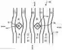
Referring now to FIGS. 1 and 2, an exemplary transistor 10 includes a drain 12, a gate 14, a source 16 and a body 18 or substrate tap. For example, the transistor 10 in FIG. 1 is an NMOS transistor. In some circumstances, the body 18 is connected to the source 16 as shown in FIG. 2.
Referring now to FIG. 3, the body 18 includes a p+ region and may include a contact tap 30. The source 16 includes an n+ region and may include a contact tap 32. The drain 12 includes an n+ region and may include a contact tap 34. Additional transistors may be fabricated on one or sides of the transistor 10 as indicated by “ . . . ” in FIG. 3.
Referring now to FIG. 4, the body 18 may be repeated between sources 16 of adjacent transistors. The body 18 takes up valuable chip area and increases the size of the transistor and the integrated circuit. Additional transistors can be arranged on one or more sides of the transistor 10 as shown by “ . . . ” in FIG. 4.
SUMMARY OF THE INVENTIONAn integrated circuit according to the present invention includes a first source, a first drain, and a first gate that is arranged between the first source and the first drain. A first body is arranged inside of and is surrounded by the first source.
In other features, the first source and the first drain include n+ regions and the body includes a p+ region. The first body tapers as a distance between a midportion of the first body and the first gate decreases. The first body has at least one of a diamond shape, a circular shape, an elliptical shape, a hexagon shape, an octagon shape and a football shape. The first body is in contact with the first gate or spaced from the first gate.
In other features, a second drain has n+ regions. A second gate is arranged between the first source and the second drain. The first and second gates are connected. The first body includes a body contact tap. The first and second gates are arranged farther apart adjacent to the first body than in areas that are not adjacent to the body contact tap. Alternately, the first source includes a source contact tap. The first and second gates are arranged farther apart adjacent to the source contact tap than in areas that are not adjacent to the source contact tap.
Further areas of applicability of the present invention will become apparent from the detailed description provided hereinafter. It should be understood that the detailed description and specific examples, while indicating the preferred embodiment of the invention, are intended for purposes of illustration only and are not intended to limit the scope of the invention.
BRIEF DESCRIPTION OF THE DRAWINGSThe present invention will become more fully understood from the detailed description and the accompanying drawings, wherein:
FIG. 1 is an electrical symbol for a transistor with a drain, source, gate and body according to the prior art;
FIG. 2 is an electrical symbol for a transistor with a drain, source, gate and body, which is connected to the source according to the prior art;
FIG. 3 is an exemplary layout of the transistor of FIG. 2 according to the prior art;
FIG. 4 is an exemplary layout of multiple transistors that are arranged in a row according to the prior art;
FIG. 5 is a first exemplary layout of transistors including a body that is arranged in the source;
FIG. 6 is a second exemplary layout of transistors including a body that is arranged in the source;
FIG. 7 is a third exemplary layout of transistors including a body that is arranged in the source;
FIG. 8 is a fourth exemplary layout of transistors including a body that is arranged in the source; and
FIG. 9 is a fifth exemplary layout of transistors including a body that is arranged in the source.
DETAILED DESCRIPTION OF THE PREFERRED EMBODIMENTSThe following description of the preferred embodiment(s) is merely exemplary in nature and is in no way intended to limit the invention, its application, or uses. For purposes of clarity, the same reference numbers will be used in the drawings to identify the same elements. Additional transistors can be arranged on one or more sides of the illustrated transistors that are shown in the FIGs. as indicated by “ . . . ” in the FIGs.
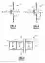
Referring now to FIG. 5, a transistor 50 according to the present invention is shown to include one or more sources 54 and one or more drains 56. The sources 54 and the drains 56 include n+ regions. While an NMOS transistor is shown, skilled artisans will appreciate that the present invention also applies to other types of transistors such as PMOS transistors. Gates 58 are located between adjacent pairs of sources 54 and drains 56. In one implementation, the gates 58 that are located on opposite sides of the sources 54 are connected together as shown at 64. In other configurations, however, the gates 58 need not be connected together.
A body 66 including a p+ region is arranged inside of and is surrounded by the source 54. The body 66 preferably has a shape that tapers as a distance between a midportion of the body 66 and adjacent gates decreases. The body 66 may touch or not touch the gates 58. By utilizing some of the area of the source 54 for the body 66, the overall size of the transistor 50 is reduced as compared to conventional transistors. In the exemplary implementation that is shown in FIG. 5, the body 66 has a diamond shape.
Referring now to FIGS. 6 and 7, other exemplary shapes for the body 66 are shown. In FIG. 6, the body 66 has a hexagon shape. In FIG. 7, the body is generally football shaped. Skilled artisans will appreciate that there are a wide variety of other suitable shapes. For example, a circular body is shown in FIG. 8, which is described. Other suitable shapes include an ellipse, an octagon, etc.
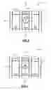
Referring now to FIGS. 8 and 9, the gates 58 can be arranged such that they are closer together when there are no contact taps and further apart when there are contact taps. In FIG. 8, a source contact tap 70, which is not located in the body 66, is located in a region where the adjacent gates 58 are located farther apart. In FIG. 9, a body contact tap 80, which is not located in the body 66, is located in the source 54 where the adjacent gates 58 are located farther apart.
Those skilled in the art can now appreciate from the foregoing description that the broad teachings of the present invention can be implemented in a variety of forms. Therefore, while this invention has been described in connection with particular examples thereof, the true scope of the invention should not be so limited since other modifications will become apparent to the skilled practitioner upon a study of the drawings, the specification and the following claims.
Claims
1. An integrated circuit comprising:
a first source;
a first drain;
a first gate that is arranged between said first source and said first drain; and
a first body that is arranged inside of and is surrounded by said first source.
2. The integrated circuit of claim 1 wherein said first source and said first drain include n+ regions and said first body includes a p+ region.
3. The integrated circuit of claim 1 wherein said first body tapers as a distance between a midportion of said first body and said first gate decreases.
4. The integrated circuit of claim 1 wherein said first body has at least one of a diamond shape, a circular shape, an elliptical shape, a hexagon shape, an octagon shape and a football shape.
5. The integrated circuit of claim 1 wherein said first body is in contact with said first gate.
6. The integrated circuit of claim 1 wherein said first body is spaced from said first gate.
7. The integrated circuit of claim 1 further comprising:
a second drain; and
a second gate that is arranged between said first source and said second drain.
8. The integrated circuit of claim 7 wherein said first and second gates are connected.
9. The integrated circuit of claim 7 wherein said first body includes a body contact tap and wherein said first and second gates are arranged farther apart adjacent to said body contact tap than in areas that are not adjacent to said body contact tap.
10. The integrated circuit of claim 7 wherein said first source includes a source contact tap and wherein said first and second gates are arranged farther apart adjacent to said source contact tap than in areas that are not adjacent to said source contact tap.
11. An integrated circuit comprising:
a first source;
a first drain;
a first gate that is arranged between said first source and said first drain;
a first body that is arranged inside of and is surrounded by said first source;
a second drain; and
a second gate that is arranged between said first source and said second drain,
wherein said first body includes a body contact tap and wherein said first and second gates are arranged farther apart adjacent to said body contact tap than in areas that are not adjacent to said body contact tap.
12. The integrated circuit of claim 11 wherein said first source, said first drain, and said second drain include n+ regions and said first body includes a p+ region.
13. The integrated circuit of claim 11 wherein said first body tapers as a distance between a midportion of said first body and said first gate decreases.
14. The integrated circuit of claim 11 wherein said first body has at least one of a diamond shape, a circular shape, an elliptical shape, a hexagon shape, an octagon shape and a football shape.
15. The integrated circuit of claim 11 wherein said first body is in contact with said first gate.
16. The integrated circuit of claim 11 wherein said first body is spaced from said first gate.
17. The integrated circuit of claim 11 wherein said first and second gates are connected.
18. An integrated circuit comprising:
a first source;
a first drain;
a first gate that is arranged between said first source and said first drain;
a first body that is arranged inside of and is surrounded by said first source;
a second drain; and
a second gate that is arranged between said first source and said second drain,
wherein said first source includes a source contact tap and wherein said first and second gates are arranged farther apart adjacent to said source contact tap than in areas that are not adjacent to said source contact tap.
19. The integrated circuit of claim 18 wherein said first source, said first drain, and said second drain include n+ regions and said first body includes a p+ region.
20. The integrated circuit of claim 18 wherein said first body tapers as a distance between a midportion of said first body and said first gate decreases.
21. The integrated circuit of claim 18 wherein said first body has at least one of a diamond shape, a circular shape, an elliptical shape, a hexagon shape, an octagon shape and a football shape.
22. The integrated circuit of claim 18 wherein said first body is in contact with said first gate.
23. The integrated circuit of claim 18 wherein said first body is spaced from said first gate.
24. The integrated circuit of claim 18 wherein said first and second gates are connected.
Images & Drawings included:


Sources:
- United States Patent and Trademark Office - verify current appl. status at the USPTO↗
Similar patent applications:
- » 20060033171
Efficient transistor structure - » 20070032063
Efficient transistor structure - » 20070034903
Efficient transistor structure - » 20070034904
Efficient transistor structure - » 20070037353
Efficient transistor structure - » 20250120175
AREA-EFFICIENT FULLY DEPLETED SEMICONDUCTOR-ON-INSULATOR STRUCTURE WITH MIXED THRESHOLD VOLTAGE TRANSISTORS
Recent applications in this class:
- » 20250072070 2025-02-27
SEMICONDUCTOR DEVICES AND METHODS OF FABRICATING THE SAME - » 20250072069 2025-02-27
RECESSED VIA WITH CONDUCTIVE LINK TO ADJACENT CONTACT - » 20250063783 2025-02-20
CONTACT STRUCTURE FOR SEMICONDUCTOR DEVICE AND METHOD - » 20250063782 2025-02-20
INTEGRATED CIRCUIT DEVICE INCLUDING WIMPY TRANSISTOR STACK WITH THICK SOURCE/DRAIN ISOLATION LAYER AND METHODS OF FORMING TING THE SAME - » 20250056852 2025-02-13
SOURCE/DRAIN REGIONS IN COMPLEMENTARY FIELD EFFECT TRANSISTORS AND METHODS OF FORMING THE SAME - » 20250048698 2025-02-06
GATE-ALL-AROUND INTEGRATED CIRCUIT STRUCTURES HAVING SOURCE OR DRAIN STRUCTURES WITH EPITAXIAL NUBS - » 20250048697 2025-02-06
SEMICONDUCTOR DEVICES INCLUDING GATE STRUCTURES AND IMPURITY REGIONS - » 20250048696 2025-02-06
SEMICONDUCTOR DEVICE AND METHOD OF FABRICATING THE SAME - » 20250048695 2025-02-06
MULTI-GATE FET WITH SELF-ALIGNED TAPERED ACTIVE REGION EDGE - » 20250048694 2025-02-06
SEMICONDUCTOR DEVICE STRUCTURE AND METHODS OF FORMING THE SAME
Recent applications for this Assignee:
- » 20200382996 2020-12-03
Methods and apparatus for distributing baseband signal processing of fifth (5G) new radio uplink signals - » 20200202894 2020-06-25
Differential interface transmission of fly-height control data - » 20200202893 2020-06-25
Zone self servo writing with synchronized parallel clocks - » 20200186342 2020-06-11
Self-encryption drive (SED) - » 20200186340 2020-06-11
Self-encryption drive (SED) - » 20200184998 2020-06-11
Reducing offset of a differential signal output by a capacitive coupling stage of a hard disk drive preamplifier - » 20200135233 2020-04-30
Thermal compensation for laser in heat assisted magnetic recording - » 20200133898 2020-04-30
Artificial intelligence-enabled management of storage media access - » 20200066706 2020-02-27
Sub-device field-effect transistor architecture for integrated circuits - » 20200066299 2020-02-27
Pulse-based writing for magnetic storage media