Deep trench structure and memory device having the same
US20050110066A1
2005-05-26
10/718,666
2003-11-24
Abstract:
Disclosed is a deep trench structure for a semiconductor memory device. The deep trench in accordance with the present invention has a cross section communicating with two difference active areas, which are respectively connected to two adjacent bit lines of the semiconductor memory device.
Assignee:
- NANYA TECHNOLOGY CORPORATION 409 🇹🇼 Taoyuan, Taiwan
Interested in similar patents?
Get notified when new applications in this technology area are published.
Classification:
H01L27/10897 » CPC further
Devices consisting of a plurality of semiconductor or other solid-state components formed in or on a common substrate including semiconductor components specially adapted for rectifying, oscillating, amplifying or switching and having at least one potential-jump barrier or surface barrier; including integrated passive circuit elements with at least one potential-jump barrier or surface barrier the substrate being a semiconductor body including a plurality of individual components in a repetitive configuration including field-effect components; Dynamic random access memory structures Peripheral structures
Description
BACKGROUND OF THE INVENTION1. Field of the Invention
The present invention relates to a semiconductor memory device, more specifically, to a deep trench structure facilitating electrical test.
2. Description of the Prior Art
In semiconductor technology, testing technique is used to detect the defects and bugs in the wafers in order to find out defective products and promote the throughput. The electrical test for the semiconductor memory device is very important. The electrical parameters of the memory device directly influence the function and performance of the memory.
In the current techniques for semiconductor memory devices, deep trench technique is generally used in a semiconductor memory device structure having compact memory cell array. Because of the buried straps in the structure, it is impossible to directly access the deep trench capacitor. Accordingly, it is difficult to measure the leakages at the buried strap side such as gate inducing drain leakage (GIDL) and junction leakage.
Therefore, there is a need for a solution to overcome the problems stated above. The present invention satisfies such a need.
SUMMARY OF THE INVENTIONAn objective of the present invention is to provide a deep trench structure of semiconductor device, which facilitates the measurement of the leakage currents.
Another objective of the present invention is to provide a semiconductor memory device, in which the leakage currents are easy to measure.
According to an aspect of the present invention, a deep trench structure of semiconductor device is characterized in that the cross section of the deep trench communicates with two different active areas of the semiconductor device.
According to another aspect of the present invention, a semiconductor memory device comprises a plurality of bit lines; a plurality of gates crossing with said bit lines; a plurality of active areas, each of which is connected with one of said bit lines; and a plurality of deep trenches, at least one of which has a cross section communicating with two different active areas.
BRIEF DESCRIPTION OF THE DRAWINGSThe following drawings are only for illustrating the mutual relationships between the respective portions and are not drawn according to practical dimensions and ratios. In addition, the like reference numbers indicate the similar elements.
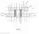
FIG. 1 shows a schematic diagram of the top view of a portion of a semiconductor memory device having a deep trench structure in accordance with the present invention; and
FIG. 2 shows the longitudinal sectional diagram taken from the path A-A in FIG. 1.
DETIALED DESCRIPTION OF THE PREFERRED EMBODIMENTAn embodiment of the present invention will be described in detail with reference to the accompanying drawings.
With reference to FIG. 1, it is a schematic diagram showing a top view of a portion of a semiconductor memory device having deep trenches in accordance with the present invention. Reference number 11 indicates a bit line, 12 indicates a gate crossing with said bit line, and the bit lines 11 and gates 12 constitute an array arrangement. Reference numbers 13, 13′ and 13″ indicate active areas connected with the bit lines, 14 indicates a conventional deep trench, while 15 indicates a deep trench in accordance with the present invention.
As shown in the drawing, the cross sections of the deep trenches 15 are lengthened, so that the two deep trenches 15 respectively communicate with active areas 13 and 13′, as well as active areas 13″ and 13′ connected with adjacent bit lines. By means of such a structure, GIDL current and junction leakage current can be easily measured through the gate 12.
FIG. 2 shows a schematic longitudinal sectional diagram taken from the path A-A in FIG. 1 for reference, wherein WL indicates a word line.
While the embodiment of the present invention is illustrated and described, various modifications and alterations can be made by persons skilled in this art. The embodiment of the present invention is therefore described in an illustrative but not restrictive sense. It is intended that the present invention may not be limited to the particular forms as illustrated, and that all modifications and alterations which maintain the spirit and realm of the present invention are within the scope as defined in the appended claims.
Claims
1. A deep trench structure of semiconductor device, said semiconductor device having a plurality of active areas, said deep trench structure characterized in that said deep trench communicates with two different active areas.
2. The structure as claimed in claim 1, wherein the cross section of said deep trench communicates with two different active areas.
3. The structure as claimed in claim 2, wherein said two different active areas communicated by said deep trench are respectively connected with two adjacent bit lines.
4. A semiconductor memory device comprising:
a plurality of bit lines;
a plurality of gates crossing with said bit lines;
a plurality of active areas, each of which is connected to one of said bit lines;
a plurality of deep trenches, at least one of which communicates with two different active areas.
5. The device as claimed in claim 4, wherein the cross section of said deep trench communicates with two different active areas.
6. The device as claimed in claim 5, wherein said two different active areas communicated by said deep trench are respectively connected with two adjacent bit lines.
Images & Drawings included:

Sources:
- United States Patent and Trademark Office - verify current appl. status at the USPTO↗
Recent applications in this class:
- » 20180294267 2018-10-11
Self aligned buried power rail - » 20170062436 2017-03-02
Trigate device with full silicided epi-less source/drain for high density access transistor applications - » 20170025418 2017-01-26
Semiconductor structures with deep trench capacitor and methods of manufacture - » 20160379986 2016-12-29
REPLACEMENT GATE MULTIGATE TRANSISTOR FOR EMBEDDED DRAM - » 20160284709 2016-09-29
Trench to trench fin short mitigation - » 20160233219 2016-08-11
Coaxial carbon nanotube capacitor for eDRAM - » 20160197083 2016-07-07
Metal strap for DRAM/FinFET combination - » 20160099249 2016-04-07
Method of forming integrated fin and strap structure for an access transistor of a trench capacitor - » 20160027788 2016-01-28
Dynamic random access memory cell with self-aligned strap - » 20150364476 2015-12-17
Semiconductor structure having buried conductive elements
Recent applications for this Assignee:
- » 20190109113 2019-04-11
Semiconductor apparatus and method for preparing the same - » 20190081018 2019-03-14
Method for preparing a semiconductor package - » 20180374818 2018-12-27
Method for preparing a semiconductor apparatus - » 20180233486 2018-08-16
Die device, semiconductor device and method for making the same - » 20180226332 2018-08-09
Package structure and manufacturing method thereof - » 20180197284 2018-07-12
Method of recognizing wafer - » 20180196769 2018-07-12
Comparative forwarding circuit providing first datum and second datum to one of first circuit and second circuit according to target address - » 20180190607 2018-07-05
Semiconductor package and method for preparing the same - » 20180182588 2018-06-28
System and method for blowing a fuse - » 20180138145 2018-05-17
Semiconductor package and manufacturing method thereof