Method of fabricating inkjet nozzles
US20050145600A1
2005-07-07
11/071,261
2005-03-04
✅ Patent granted
US 7,175,774 B2
2007-02-13
-
-
Allan Olsen
2025-03-04
Abstract:
A method of fabricating inkjet nozzles on a substrate is provided. Each nozzle comprises a nozzle chamber and an actuator positioned in the nozzle chamber. Each nozzle chamber comprises a roof having a nozzle aperture defined therein and sidewalls extending from the roof to the substrate. The method comprises the steps of: (a) depositing a layer of first sacrificial material onto the substrate; (b) defining actuator scaffolds in the first sacrificial material (c) depositing actuator material onto the actuator scaffolds; (d) etching the actuator material to define actuators; (e) depositing a layer of second sacrificial material onto the actuators, the first sacrificial material and/or the substrate; (f) defining openings in the second sacrificial material, the openings being complementary to chamber sidewalls; (g) depositing roof material onto the sacrificial material and into the openings, thereby forming the roof and sidewalls of each chamber; (h) etching nozzle apertures through each roof; and (i) removing the first and second sacrificial materials exposed through the nozzle apertures.
Assignee:
- Silverbrook Research Pty Ltd 922 🇦🇺 Balmain, Australia
Interested in similar patents?
Get notified when new applications in this technology area are published.
Classification:
G01D15/00 IPC
Component parts of recorders for measuring arrangements not specially adapted for a specific variable
G11B5/127 IPC
Recording by magnetisation or demagnetisation of a record carrier; Reproducing by magnetic means; Record carriers therefor Structure or manufacture of heads, e.g. inductive
B41J2/17513 » CPC main
Typewriters or selective printing mechanisms characterised by the printing or marking process for which they are designed characterised by bringing liquid or particles selectively into contact with a printing material; Ink jet characterised by ink handling; Ink supply systems ; Circuit parts therefor; Ink cartridges Inner structure
B41J2/14 » CPC further
Typewriters or selective printing mechanisms characterised by the printing or marking process for which they are designed characterised by bringing liquid or particles selectively into contact with a printing material; Ink jet; Nozzles Structure thereof only for on-demand ink jet heads
B41J2/14314 » CPC further
Typewriters or selective printing mechanisms characterised by the printing or marking process for which they are designed characterised by bringing liquid or particles selectively into contact with a printing material; Ink jet; Nozzles; Structure thereof only for on-demand ink jet heads Structure of ink jet print heads with electrostatically actuated membrane
B41J2/14427 » CPC further
Typewriters or selective printing mechanisms characterised by the printing or marking process for which they are designed characterised by bringing liquid or particles selectively into contact with a printing material; Ink jet; Nozzles; Structure thereof only for on-demand ink jet heads Structure of ink jet print heads with thermal bend detached actuators
B41J2/16 » CPC further
Typewriters or selective printing mechanisms characterised by the printing or marking process for which they are designed characterised by bringing liquid or particles selectively into contact with a printing material; Ink jet; Nozzles Production of nozzles
B41J2/1623 » CPC further
Typewriters or selective printing mechanisms characterised by the printing or marking process for which they are designed characterised by bringing liquid or particles selectively into contact with a printing material; Ink jet; Nozzles; Production of nozzles manufacturing processes bonding and adhesion
B41J2/1626 » CPC further
Typewriters or selective printing mechanisms characterised by the printing or marking process for which they are designed characterised by bringing liquid or particles selectively into contact with a printing material; Ink jet; Nozzles; Production of nozzles manufacturing processes etching
B41J2/1631 » CPC further
Typewriters or selective printing mechanisms characterised by the printing or marking process for which they are designed characterised by bringing liquid or particles selectively into contact with a printing material; Ink jet; Nozzles; Production of nozzles manufacturing processes photolithography
B41J2/1632 » CPC further
Typewriters or selective printing mechanisms characterised by the printing or marking process for which they are designed characterised by bringing liquid or particles selectively into contact with a printing material; Ink jet; Nozzles; Production of nozzles manufacturing processes machining
B41J2/1635 » CPC further
Typewriters or selective printing mechanisms characterised by the printing or marking process for which they are designed characterised by bringing liquid or particles selectively into contact with a printing material; Ink jet; Nozzles; Production of nozzles manufacturing processes dividing the wafer into individual chips
B41J2/1637 » CPC further
Typewriters or selective printing mechanisms characterised by the printing or marking process for which they are designed characterised by bringing liquid or particles selectively into contact with a printing material; Ink jet; Nozzles; Production of nozzles manufacturing processes molding
B41J2/1648 » CPC further
Typewriters or selective printing mechanisms characterised by the printing or marking process for which they are designed characterised by bringing liquid or particles selectively into contact with a printing material; Ink jet; Nozzles; Production of nozzles Production of print heads with thermal bend detached actuators
G06F21/79 » CPC further
Security arrangements for protecting computers, components thereof, programs or data against unauthorised activity; Protecting specific internal or peripheral components, in which the protection of a component leads to protection of the entire computer to assure secure storage of data in semiconductor storage media, e.g. directly-addressable memories
G06F21/86 » CPC further
Security arrangements for protecting computers, components thereof, programs or data against unauthorised activity; Protecting specific internal or peripheral components, in which the protection of a component leads to protection of the entire computer Secure or tamper-resistant housings
G06K1/121 » CPC further
Methods or arrangements for marking the record carrier in digital fashion otherwise than by punching by printing code marks
G06K7/14 » CPC further
Methods or arrangements for sensing record carriers, e.g. for reading patterns by electromagnetic radiation, e.g. optical sensing; by corpuscular radiation using light without selection of wavelength, e.g. sensing reflected white light
G06K7/1417 » CPC further
Methods or arrangements for sensing record carriers, e.g. for reading patterns by electromagnetic radiation, e.g. optical sensing; by corpuscular radiation using light without selection of wavelength, e.g. sensing reflected white light; Methods for optical code recognition the method being specifically adapted for the type of code 2D bar codes
G06K19/06037 » CPC further
Record carriers for use with machines and with at least a part designed to carry digital markings characterised by the kind of the digital marking, e.g. shape, nature, code with optically detectable marking multi-dimensional coding
G07F7/08 » CPC further
Mechanisms actuated by objects other than coins to free or to actuate vending, hiring, coin or paper currency dispensing or refunding apparatus by coded identity card or credit card or other personal identification means
G07F7/086 » CPC further
Mechanisms actuated by objects other than coins to free or to actuate vending, hiring, coin or paper currency dispensing or refunding apparatus by coded identity card or credit card or other personal identification means by passive credit-cards adapted therefor, e.g. constructive particularities to avoid counterfeiting, e.g. by inclusion of a physical or chemical security-layer
G07F7/12 » CPC further
Mechanisms actuated by objects other than coins to free or to actuate vending, hiring, coin or paper currency dispensing or refunding apparatus by coded identity card or credit card or other personal identification means Card verification
G11C11/56 » CPC further
Digital stores characterised by the use of particular electric or magnetic storage elements; Storage elements therefor using storage elements with more than two stable states represented by steps, e.g. of voltage, current, phase, frequency
H04N5/225 » CPC further
Details of television systems; Studio circuitry; Studio devices; Studio equipment ; Cameras comprising an electronic image sensor, e.g. digital cameras, video cameras, TV cameras, video cameras, camcorders, webcams, camera modules for embedding in other devices, e.g. mobile phones, computers or vehicles Television cameras ; Cameras comprising an electronic image sensor, e.g. digital cameras, video cameras, camcorders, webcams, camera modules specially adapted for being embedded in other devices, e.g. mobile phones, computers or vehicles
H04N5/2628 » CPC further
Details of television systems; Studio circuitry; Studio devices; Studio equipment ; Cameras comprising an electronic image sensor, e.g. digital cameras, video cameras, TV cameras, video cameras, camcorders, webcams, camera modules for embedding in other devices, e.g. mobile phones, computers or vehicles; Studio circuits, e.g. for mixing, switching-over, change of character of image, other special effects ; Cameras specially adapted for the electronic generation of special effects Alteration of picture size, shape, position or orientation, e.g. zooming, rotation, rolling, perspective, translation
B41J2/16585 » CPC further
Typewriters or selective printing mechanisms characterised by the printing or marking process for which they are designed characterised by bringing liquid or particles selectively into contact with a printing material; Ink jet; Nozzles; Preventing or detecting of nozzle clogging, e.g. cleaning, capping or moistening for nozzles for paper-width or non-reciprocating print heads
B41J2/17596 » CPC further
Typewriters or selective printing mechanisms characterised by the printing or marking process for which they are designed characterised by bringing liquid or particles selectively into contact with a printing material; Ink jet characterised by ink handling; Ink supply systems ; Circuit parts therefor Ink pumps, ink valves
B41J2002/041 » CPC further
Typewriters or selective printing mechanisms characterised by the printing or marking process for which they are designed characterised by bringing liquid or particles selectively into contact with a printing material; Ink jet characterised by the jet generation process generating single droplets or particles on demand Electromagnetic transducer
B41J2002/14346 » CPC further
Typewriters or selective printing mechanisms characterised by the printing or marking process for which they are designed characterised by bringing liquid or particles selectively into contact with a printing material; Ink jet; Nozzles; Structure thereof only for on-demand ink jet heads Ejection by pressure produced by thermal deformation of ink chamber, e.g. buckling
B41J2002/14435 » CPC further
Typewriters or selective printing mechanisms characterised by the printing or marking process for which they are designed characterised by bringing liquid or particles selectively into contact with a printing material; Ink jet; Nozzles; Structure thereof only for on-demand ink jet heads; Structure of ink jet print heads with thermal bend detached actuators Moving nozzle made of thermal bend detached actuator
B41J2002/14443 » CPC further
Typewriters or selective printing mechanisms characterised by the printing or marking process for which they are designed characterised by bringing liquid or particles selectively into contact with a printing material; Ink jet; Nozzles; Structure thereof only for on-demand ink jet heads; Structure of ink jet print heads with thermal bend detached actuators Nozzle guard
B41J2202/21 » CPC further
Embodiments of or processes related to ink-jet or thermal heads; Embodiments of or processes related to ink-jet heads Line printing
G06F2221/2129 » CPC further
Indexing scheme relating to security arrangements for protecting computers, components thereof, programs or data against unauthorised activity; Indexing scheme relating to and subgroups addressing additional information or applications relating to security arrangements for protecting computers, components thereof, programs or data against unauthorised activity Authenticate client device independently of the user
Y10T29/49083 » CPC further
Metal working; Method of mechanical manufacture; Electrical device making; Resistor making Heater type
Y10T29/49117 » CPC further
Metal working; Method of mechanical manufacture; Electrical device making Conductor or circuit manufacturing
Y10T29/49128 » CPC further
Metal working; Method of mechanical manufacture; Electrical device making; Conductor or circuit manufacturing; On flat or curved insulated base, e.g., printed circuit, etc. Assembling formed circuit to base
Y10T29/49169 » CPC further
Metal working; Method of mechanical manufacture; Electrical device making; Conductor or circuit manufacturing Assembling electrical component directly to terminal or elongated conductor
Y10T29/49172 » CPC further
Metal working; Method of mechanical manufacture; Electrical device making; Conductor or circuit manufacturing; Assembling electrical component directly to terminal or elongated conductor with encapsulating by molding of insulating material
Y10T29/49401 » CPC further
Metal working; Method of mechanical manufacture Fluid pattern dispersing device making, e.g., ink jet
Description
CROSS REFERENCES TO RELATED APPLICATIONSThis is a divisional application of U.S. Ser. No. 10/407,212 filed on Apr. 7, 2003, which is a continuation application of U.S. Ser. No. 09/113,122 filed on Jul. 10, 1998, now issued U.S. Pat. No. 6,557,977, the entire contents of which are herein incorporated by reference.
The following Australian provisional patent applications are hereby incorporated by reference. For the purposes of location and identification, US patents/patent applications identified by their US patent/patent application serial numbers are listed alongside the Australian applications from which the US patents/patent applications claim the right of priority.
| US PATENT/PATENT | ||
| CROSS-REFERENCED | APPLICATION (CLAIMING | |
| AUSTRALIAN PRO- | RIGHT OF PRIORITY | |
| VISIONAL PATENT | FROM AUSTRALIAN PRO- | DOCKET |
| APPLICATION NO. | VISIONAL APPLICATION) | NO. |
| PO7991 | 6,750,901 | ART01 |
| PO8505 | 6,476,863 | ART02 |
| PO7988 | 6,788,336 | ART03 |
| PO9395 | 6,322,181 | ART04 |
| PO8017 | 6,597,817 | ART06 |
| PO8014 | 6,227,648 | ART07 |
| PO8025 | 6,727,948 | ART08 |
| PO8032 | 6,690,419 | ART09 |
| PO7999 | 6,727,951 | ART10 |
| PO7998 | 09/112,742 | ART11 |
| PO8031 | 09/112,741 | ART12 |
| PO8030 | 6,196,541 | ART13 |
| PO7997 | 6,195,150 | ART15 |
| PO7979 | 6,362,868 | ART16 |
| PO8015 | 09/112,738 | ART17 |
| PO7978 | 6831681 | ART18 |
| PO7982 | 6,431,669 | ART19 |
| PO7989 | 6,362,869 | ART20 |
| PO8019 | 6,472,052 | ART21 |
| PO7980 | 6,356,715 | ART22 |
| PO8018 | 09/112,777 | ART24 |
| PO7938 | 6,636,216 | ART25 |
| PO8016 | 6,366,693 | ART26 |
| PO8024 | 6,329,990 | ART27 |
| PO7940 | 09/113,072 | ART28 |
| PO7939 | 6,459,495 | ART29 |
| PO8501 | 6,137,500 | ART30 |
| PO8500 | 6,690,416 | ART31 |
| PO7987 | 09/113,071 | ART32 |
| PO8022 | 6,398,328 | ART33 |
| PO8497 | 09/113,090 | ART34 |
| PO8020 | 6,431,704 | ART38 |
| PO8023 | 09/113,222 | ART39 |
| PO8504 | 09/112,786 | ART42 |
| PO8000 | 6,415,054 | ART43 |
| PO7977 | 09/112,782 | ART44 |
| PO7934 | 6,665,454 | ART45 |
| PO7990 | 6,542,645 | ART46 |
| PO8499 | 6,486,886 | ART47 |
| PO8502 | 6,381,361 | ART48 |
| PO7981 | 6,317,192 | ART50 |
| PO7986 | 6850274 | ART51 |
| PO7983 | 09/113,054 | ART52 |
| PO8026 | 6,646,757 | ART53 |
| PO8027 | 09/112,759 | ART54 |
| PO8028 | 6,624,848 | ART56 |
| PO9394 | 6,357,135 | ART57 |
| PO9396 | 09/113,107 | ART58 |
| PO9397 | 6,271,931 | ART59 |
| PO9398 | 6,353,772 | ART60 |
| PO9399 | 6,106,147 | ART61 |
| PO9400 | 6,665,008 | ART62 |
| PO9401 | 6,304,291 | ART63 |
| PO9402 | 09/112,788 | ART64 |
| PO9403 | 6,305,770 | ART65 |
| PO9405 | 6,289,262 | ART66 |
| PP0959 | 6,315,200 | ART68 |
| PP1397 | 6,217,165 | ART69 |
| PP2370 | 6,786,420 | DOT01 |
| PP2371 | 09/113,052 | DOT02 |
| PO8003 | 6,350,023 | Fluid01 |
| PO8005 | 6,318849 | Fluid02 |
| PO8066 | 6,227,652 | IJ01 |
| PO8072 | 6,213,588 | IJ02 |
| PO8040 | 6,213,589 | IJ03 |
| PO8071 | 6,231,163 | IJ04 |
| PO8047 | 6,247,795 | IJ05 |
| PO8035 | 6,394,581 | IJ06 |
| PO8044 | 6,244,691 | IJ07 |
| PO8063 | 6,257,704 | IJ08 |
| PO8057 | 6,416,168 | IJ09 |
| PO8056 | 6,220,694 | IJ10 |
| PO8069 | 6,257,705 | IJ11 |
| PO8049 | 6,247,794 | IJ12 |
| PO8036 | 6,234,610 | IJ13 |
| PO8048 | 6,247,793 | IJ14 |
| PO8070 | 6,264,306 | IJ15 |
| PO8067 | 6,241,342 | IJ16 |
| PO8001 | 6,247,792 | IJ17 |
| PO8038 | 6,264,307 | IJ18 |
| PO8033 | 6,254,220 | IJ19 |
| PO8002 | 6,234,611 | IJ20 |
| PO8068 | 6,302,528 | IJ21 |
| PO8062 | 6,283.582 | IJ22 |
| PO8034 | 6,239,821 | IJ23 |
| PO8039 | 6,338,547 | IJ24 |
| PO8041 | 6,247,796 | IJ25 |
| PO8004 | 6,557,977 | IJ26 |
| PO8037 | 6,390,603 | IJ27 |
| PO8043 | 6,362,843 | IJ28 |
| PO8042 | 6,293,653 | IJ29 |
| PO8064 | 6,312,107 | IJ30 |
| PO9389 | 6,227,653 | IJ31 |
| PO9391 | 6,234,609 | IJ32 |
| PP0888 | 6,238,040 | IJ33 |
| PP0891 | 6,188,415 | IJ34 |
| PP0890 | 6,227,654 | IJ35 |
| PP0873 | 6,209,989 | IJ36 |
| PP0993 | 6,247,791 | IJ37 |
| PP0890 | 6,336,710 | IJ38 |
| PP1398 | 6,217,153 | IJ39 |
| PP2592 | 6,416,167 | IJ40 |
| PP2593 | 6,243,113 | IJ41 |
| PP3991 | 6,283,581 | IJ42 |
| PP3987 | 6,247,790 | IJ43 |
| PP3985 | 6,260,953 | IJ44 |
| PP3983 | 6,267,469 | IJ45 |
| PO7935 | 6,224,780 | IJM01 |
| PO7936 | 6,235,212 | IJM02 |
| PO7937 | 6,280,643 | IJM03 |
| PO8061 | 6,284,147 | IJM04 |
| PO8054 | 6,214,244 | IJM05 |
| PO8065 | 6,071,750 | IJM06 |
| PO8055 | 6,267,905 | IJM07 |
| PO8053 | 6,251,298 | IJM08 |
| PO8078 | 6,258,285 | IJM09 |
| PO7933 | 6,225,138 | IJM10 |
| PO7950 | 6,241,904 | IJM11 |
| PO7949 | 6,299,786 | IJM12 |
| PO8060 | 09/113,124 | IJM13 |
| PO8059 | 6,231,773 | IJM14 |
| PO8073 | 6,190,931 | IJM15 |
| PO8076 | 6,248,249 | IJM16 |
| PO8075 | 6,290,862 | IJM17 |
| PO8079 | 6,241,906 | IJM18 |
| PO8050 | 6,565,762 | IJM19 |
| PO8052 | 6,241,905 | IJM20 |
| PO7948 | 6,451,216 | IJM21 |
| PO7951 | 6,231,772 | IJM22 |
| PO8074 | 6,274,056 | IJM23 |
| PO7941 | 6,290,861 | IJM24 |
| PO8077 | 6,248,248 | IJM25 |
| PO8058 | 6,306,671 | IJM26 |
| PO8051 | 6,331,258 | IJM27 |
| PO8045 | 6,111,754 | IJM28 |
| PO7952 | 6,294,101 | IJM29 |
| PO8046 | 6,416,679 | IJM30 |
| PO9390 | 6,264,849 | IJM31 |
| PO9392 | 6,254,793 | IJM32 |
| PP0889 | 6,235,211 | IJM35 |
| PP0887 | 6,491,833 | IJM36 |
| PP0882 | 6,264,850 | IJM37 |
| PP0874 | 6,258,284 | IJM38 |
| PP1396 | 6,312,615 | IJM39 |
| PP3989 | 6,228,668 | IJM40 |
| PP2591 | 6,180,427 | IJM41 |
| PP3990 | 6,171,875 | IJM42 |
| PP3986 | 6,267,904 | IJM43 |
| PP3984 | 6,245,247 | IJM44 |
| PP3982 | 6,315,914 | IJM45 |
| PP0895 | 6,231,148 | IR01 |
| PP0870 | 09/113,106 | IR02 |
| PP0869 | 6,293,658 | IR04 |
| PP0887 | 6,614,560 | IR05 |
| PP0885 | 6,238,033 | IR06 |
| PP0884 | 6,312,070 | IR10 |
| PP0886 | 6,238,111 | IR12 |
| PP0871 | 09/113,086 | IR13 |
| PP0876 | 09/113,094 | IR14 |
| PP0877 | 6,378,970 | IR16 |
| PP0878 | 6,196,739 | IR17 |
| PP0879 | 09/112,774 | IR18 |
| PP0883 | 6,270,182 | IR19 |
| PP0880 | 6,152,619 | IR20 |
| PP0881 | 09/113,092 | IR21 |
| PO8006 | 6,087,638 | MEMS02 |
| PO8007 | 6,340,222 | MEMS03 |
| PO8008 | 09/113,062 | MEMS04 |
| PO8010 | 6,041,600 | MEMS05 |
| PO8011 | 6,299,300 | MEMS06 |
| PO7947 | 6,067,797 | MEMS07 |
| PO7944 | 6,286,935 | MEMS09 |
| PO7946 | 6,044,646 | MEMS10 |
| PO9393 | 09/113,065 | MEMS11 |
| PP0875 | 09/113,078 | MEMS12 |
| PP0894 | 6,382,769 | MEMS13 |
Not applicable.
FIELD OF THE INVENTIONThe present invention relates to an ink jet printer device.
BACKGROUND OF THE INVENTIONMany different types of printing have been invented, a large number of which are presently in use. The known forms of print have a variety of methods for marking the print media with a relevant marking media. Commonly used forms of printing include offset printing, laser printing and copying devices, dot matrix type impact printers, thermal paper printers, film recorders, thermal wax printers, dye sublimation printers and ink jet printers both of the drop on demand and continuous flow type. Each type of printer has its own advantages and problems when considering cost, speed, quality, reliability, simplicity of construction and operation etc.
In recent years, the field of ink jet printing, wherein each individual pixel of ink is derived from one or more ink nozzles has become increasingly popular primarily due to its inexpensive and versatile nature.
Many different techniques of ink jet printing have been invented. For a survey of the field, reference is made to an article by J Moore, “Non-Impact Printing: Introduction and Historical Perspective”, Output Hard Copy Devices, Editors R Dubeck and S Sherr, pages 207-220 (1988).
Ink Jet printers themselves come in many different forms. The utilization of a continuous stream of ink in ink jet printing appears to date back to at least 1929 wherein U.S. Pat. No. 1,941,001 by Hansell discloses a simple form of continuous stream electrostatic ink jet printing.
U.S. Pat. No. 3,596,275 by Sweet also discloses a process of continuous ink jet printing including a step wherein the ink jet stream is modulated by a high frequency electro-static field so as to cause drop separation. This technique is still utilized by several manufacturers including Elmjet and Scitex (see also U.S. Pat. No. 3,373,437 by Sweet et al).
Piezoelectric ink jet printers are also one form of commonly utilized ink jet printing device. Piezoelectric systems are disclosed by Kyser et. al. in U.S. Pat. No. 3,946,398 (1970) which utilizes a diaphragm mode of operation, by Zolten in U.S. Pat. No. 3,683,212 (1970) which discloses a squeeze mode of operation of a piezoelectric crystal, Stemme in U.S. Pat. No. 3,747,120 (1972) discloses a bend mode of piezoelectric operation, Howkins in U.S. Pat. No. 4,459,601 discloses a piezoelectric push mode actuation of the ink jet stream and Fischbeck in U.S. Pat. No. 4,584,590 which discloses a shear mode type of piezoelectric transducer element.
Recently, thermal inkjet printing has become an extremely popular form of inkjet printing. The inkjet printing techniques include those disclosed by Endo et al in GB 2007162 (1979) and Vaught et al in U.S. Pat. No. 4,490,728. Both the aforementioned references disclose ink jet printing techniques which rely upon the activation of an electrothermal actuator which results in the creation of a bubble in a constricted space, such as a nozzle, which thereby causes the ejection of ink from an aperture connected to the confined space onto a relevant print media. Printing devices utilizing the electro-thermal actuator are manufactured by manufacturers such as Canon and Hewlett Packard.
As can be seen from the foregoing, many different types of printing technologies are available. Ideally, a printing technology should have a number of desirable attributes. These include inexpensive construction and operation, high speed operation, safe and continuous long term operation etc. Each technology may have its own advantages and disadvantages in the areas of cost, speed, quality, reliability, power usage, simplicity of construction operation, durability and consumables.
It would be desirable to create a more compact and efficient inkjet printer having an efficient and effective operation in addition to being as compact as possible.
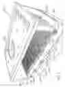
BRIEF DESCRIPTION OF THE DRAWINGSFIG. 1 is a perspective view partly in sections of a single ink jet nozzle constructed in accordance with a preferred embodiment;
FIG. 2 is an exploded perspective view partly in section illustrating the construction of a single ink nozzle in accordance with a preferred embodiment of the present invention;
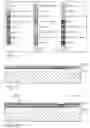
FIG. 3 provides a legend of the materials indicated in FIG. 4 to 16;
FIG. 4 to FIG. 16 illustrate sectional views of the manufacturing steps in one form of construction of an ink jet printhead nozzle;
DESCRIPTION OF PREFERRED AND OTHER EMBODIMENTSThe ink jet designs shown here are suitable for a wide range of digital printing systems, from battery powered one-time use digital cameras, through to desktop and network printers, and through to commercial printing systems For ease of manufacture using standard process equipment, the print head is designed to be a monolithic CMOS chip with MEMS post processing. For a general introduction to micro-electric mechanical systems (MEMS) reference is made to standard proceedings in this field including the proceedings of the SPIE (International Society for Optical Engineering), volumes 2642 and 2882 which contain the proceedings for recent advances and conferences in this field.
For color photographic applications, the print head is 100 mm long, with a width which depends upon the ink jet type.
IJ27
In a preferred embodiment, a “roof shooting” ink jet printhead is constructed utilizing a buckle plate actuator for the ejection of ink. In a preferred embodiment, the buckle plate actuator is constructed from polytetrafluoroethylene (PTFE) which provides superior thermal expansion characteristics. The PTFE is heated by an integral, serpentine shaped heater, which preferably is constructed from a resistive material, such as copper.
Turning now to FIG. 1 there is shown a sectional perspective view of an ink jet printhead 2701 of a preferred embodiment. The ink jet printhead includes a nozzle chamber 2702 in which ink is stored to be ejected. The chamber 2702 can be independently connected to an ink supply (not shown) for the supply and refilling of the chamber. At the base of the chamber 2702 is a buckle plate 2703 which comprises a heater element 2704 which can be of an electrically resistive material such as copper. The heater element 2704 is encased in a polytetrafluoroethylene layer 2705. The utilization of the PTFE layer 2705 allows for high rates of thermal expansion and therefore more effective operation of the buckle plate 2703. PTFE has a high coefficient of thermal expansion (770×10−6) with the copper having a much lower degree of thermal expansion. The copper heater element 2704 is therefore fabricated in a serpentine pattern so as to allow the expansion of the PTFE layer to proceed unhindered. The serpentine fabrication of the heater element 2704 means that the two coefficients of thermal expansion of the PTFE and the heater material need not be closely matched. The PTFE is primarily chosen for its high thermal expansion properties.
Current can be supplied to the buckle plate 2703 by means of connectors 2707, 2708 which inter-connect the buckle plate 2703 with a lower drive circuitry and logic layer 2726. Hence, to operate the ink jet head 2701, the heater coil 2704 is energized thereby heating the PTFE 2705. The PTFE 2705 expands and buckles between end portions 2712, 2713. The buckle causes initial ejection of ink out of a nozzle 2715 located at the top of the nozzle chamber 2702. There is an air bubble between the buckle plate 2703 and the adjacent wall of the chamber which forms due to the hydrophobic nature of the PTFE on the back surface of the buckle plate 2703. An air vent 2717 connects the air bubble to the ambient air through a channel 2718 formed between a nitride layer 2719 and an additional PTFE layer 2720, separated by posts, e.g. 2721, and through holes, e.g. 2722, in the PTFE layer 2720. The air vent 2717 allows the buckle plate 2703 to move without being held back by a reduction in air pressure as the buckle plate 2703 expands. Subsequently, power is turned off to the buckle plate 2703 resulting in a collapse of the buckle plate and the sucking back of some of the ejected ink. The forward motion of the ejected ink and the sucking back is resolved by an ink drop breaking off from the main volume of ink and continuing onto a page. Ink refill is then achieved by surface tension effects across the nozzle part 2715 and a resultant inflow of ink into the nozzle chamber 2702 through the grilled supply channel 2716.
Subsequently the nozzle chamber 2702 is ready for refiring.
It has been found in simulations of a preferred embodiment that the utilization of the PTFE layer and serpentine heater arrangement allows for a substantial reduction in energy requirements of operation in addition to a more compact design.
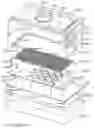
Turning now to FIG. 2, there is provided an exploded perspective view partly in section illustrating the construction of a single ink jet nozzle in accordance with a preferred embodiment. The nozzle arrangement 2701 is fabricated on top of a silicon wafer 2725. The nozzle arrangement 2701 can be constructed on the silicon wafer 2725 utilizing standard semi-conductor processing techniques in addition to those techniques commonly used for the construction of micro-electro-mechanical systems (MEMS).
On top of the silicon layer 2725 is deposited a two level CMOS circuitry layer 2726 which substantially comprises glass, in addition to the usual metal layers. Next a nitride layer 2719 is deposited to protect and passivate the underlying layer 2726. The nitride layer 2719 also includes vias for the interconnection of the heater element 2704 to the CMOS layer 2726. Next, a PTFE layer 2720 is constructed having the aforementioned holes, e.g. 2722, and posts, e.g. 2721. The structure of the PTFE layer 2720 can be formed by first laying down a sacrificial glass layer (not shown) onto which the PTFE layer 2720 is deposited. The PTFE layer 2720 includes various features, for example, a lower ridge portion 2727 in addition to a hole 2728 which acts as a via for the subsequent material layers. The buckle plate 2703 (FIG. 1) comprises a conductive layer 2731 and a PTFE layer 2732. A first, thicker PTFE layer is deposited onto a sacrificial layer (not shown). Next, a conductive layer 2731 is deposited including contacts 2729, 2730. The conductive layer 2731 is then etched to form a serpentine pattern. Next, a thinner, second PTFE layer is deposited to complete the buckle plate 2703 (FIG. 1) structure.
Finally, a nitride layer can be deposited to form the nozzle chamber proper. The nitride layer can be formed by first laying down a sacrificial glass layer and etching this to form walls, e.g. 2733, and grilled portions, e.g. 2734. Preferably, the mask utilized results in a first anchor portion 2735 which mates with the hole 2728 in layer 2720. Additionally, the bottom surface of the grill, for example 2734 meets with a corresponding step 2736 in the PTFE layer 2732. Next, a top nitride layer 2737 can be formed having a number of holes, e.g. 2738, and nozzle port 2715 around which a rim 2739 can be etched through etching of the nitride layer 2737. Subsequently the various sacrificial layers can be etched away so as to release the structure of the thermal actuator and the air vent channel 2718 (FIG. 1).
One form of detailed manufacturing process which can be used to fabricate monolithic ink jet print heads operating in accordance with the principles taught by the present embodiment can proceed utilizing the following steps:
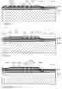
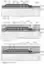
1. Using a double sided polished wafer 2725, complete drive transistors, data distribution, and timing circuits using a 0.5 micron, one poly, 2 metal CMOS process 2726. Relevant features of the wafer 2725 at this step are shown in FIG. 4. For clarity, these diagrams may not be to scale, and may not represent a cross section though any single plane of the nozzle. FIG. 3 is a key to representations of various materials in these manufacturing diagrams, and those of other cross referenced inkjet configurations.
2. Deposit 1 micron of low stress nitride 2719. This acts as a barrier to prevent ink diffusion through the silicon dioxide of the chip surface.
3. Deposit 2 microns of sacrificial material 2750 (e.g. polyimide).
4. Etch the sacrificial layer 2750 using Mask 1. This mask defines the PTFE venting layer support pillars 2721 (FIG. 1) and anchor point. This step is shown in FIG. 5.
5. Deposit 2 microns of PTFE 2720.
6. Etch the PTFE 2720 using Mask 2. This mask defines the edges of the PTFE venting layer, and the holes 2722 in this layer 2720. This step is shown in FIG. 6.
7. Deposit 3 microns of sacrificial material 2751.
8. Etch the sacrificial layer 2751 using Mask 3. This mask defines the anchor points 2712, 2713 at both ends of the buckle actuator. This step is shown in FIG. 7.
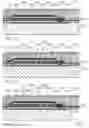
9. Deposit 1.5 microns of PTFE 2731.
10. Deposit and pattern resist using Mask 4. This mask defines the heater.
11. Deposit 0.5 microns of gold 2704 (or other heater material with a low Young's modulus) and strip the resist. Steps 10 and 11 form a lit-off process. This step is shown in FIG. 8.
12. Deposit 0.5 microns of PTFE 2732.
13. Etch the PTFE 2732 down to the sacrificial layer 2751 using Mask 5. This mask defines the actuator paddle 2703 (See FIG. 1) and the bond pads. This step is shown in FIG. 9.
14. Wafer probe. All electrical connections are complete at this point, and the chips are not yet separated.
15. Plasma process the PTFE to make the top and side surfaces of the buckle actuator hydrophilic. This allows the nozzle chamber to fill by capillarity.
16. Deposit 10 microns of sacrificial material 2752.
17. Etch the sacrificial material 2752 down to nitride 2719 using Mask 6. This mask defines the nozzle chamber 2702. This step is shown in FIG. 10.
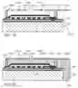
18. Deposit 3 microns of PECVD glass 2737. This step is shown in FIG. 11.
19. Etch to a depth of 1 micron using Mask 7. This mask defines the nozzle rim 2739. This step is shown in FIG. 12.
20. Etch down to the sacrificial layer 2752 using Mask 8. This mask defines the nozzle 2715 and the sacrificial etch access holes 2738. This step is shown in FIG. 13.
21. Back-etch completely through the silicon wafer 2725 (with, for example, an ASE Advanced Silicon Etcher from Surface Technology Systems) using Mask 9. This mask defines the ink inlets 2753 which are etched through the wafer 2725. The wafer 2725 is also diced by this etch. This step is shown in FIG. 14.
22. Back-etch the CMOS oxide layers 2726 and subsequently deposited nitride layers 2719 and sacrificial layer 2750, 2751 through to PTFE 2720, 2732 using the back-etched silicon as a mask.
23. Etch the sacrificial material 2752. The nozzle chambers are cleared, the actuators freed, and the chips are separated by this etch. This step is shown in FIG. 15.
24. Mount the printheads in their packaging, which may be a molded plastic former incorporating ink channels which supply the appropriate color ink to the ink inlets at the back of the wafer.
25. Connect the printheads to their interconnect systems. For a low profile connection with minimum disruption of airflow, TAB may be used. Wire bonding may also be used if the printer is to be operated with sufficient clearance to the paper.
26. Hydrophobize the front surface of the printheads.
27. Fill the completed printheads with ink 2754 and test them. A filled nozzle is shown in FIG. 16.
The presently disclosed ink jet printing technology is potentially suited to a wide range of printing system including: color and monochrome office printers, short run digital printers, high speed digital printers, offset press supplemental printers, low cost scanning printers high speed pagewidth printers, notebook computers with inbuilt pagewidth printers, portable color and monochrome printers, color and monochrome copiers, color and monochrome facsimile machines, combined printer, facsimile and copying machines, label printers, large format plotters, photograph copiers, printers for digital photographic “minilabs”, video printers, PHOTO CD (PHOTO CD is a registered trademark of the Eastman Kodak Company) printers, portable printers for PDAs, wallpaper printers, indoor sign printers, billboard printers, fabric printers, camera printers and fault tolerant commercial printer arrays.
It would be appreciated by a person skilled in the art that numerous variations and/or modifications may be made to the present invention as shown in the specific embodiments without departing from the spirit or scope of the invention as broadly described. The present embodiments are, therefore, to be considered in all respects to be illustrative and not restrictive.
Claims
1. A method of fabricating inkjet nozzles on a substrate, each nozzle comprising a nozzle chamber and an actuator positioned in the nozzle chamber, each nozzle chamber comprising a roof having a nozzle aperture defined therein and sidewalls extending from the roof to the substrate, the method comprising the steps of:
(a) depositing a layer of first sacrificial material onto the substrate;
(b) defining actuator scaffolds in the first sacrificial material
(c) depositing actuator material onto the actuator scaffolds;
(d) etching the actuator material to define actuators;
(e) depositing a layer of second sacrificial material onto the actuators, the first sacrificial material and/or the substrate;
(f) defining openings in the second sacrificial material, the openings being complementary to chamber sidewalls;
(g) depositing roof material onto the sacrificial material and into the openings, thereby forming the roof and sidewalls of each chamber;
(h) etching nozzle apertures through each roof; and
(i) removing the first and second sacrificial materials exposed through the nozzle apertures.
2. The method of claim 1, which forms part of a printhead fabrication process.
3. The method of claim 1, wherein the actuator is a thermal actuator.
4. The method of claim 1, wherein each chamber roof forms part of a nozzle plate spanning a plurality of nozzles.
5. The method of claim 1, wherein the roof material is a glass material.
6. The method of claim 1, wherein the roof material is silicon nitride.
7. The method of claim 1, wherein the roof material is deposited by plasma enhanced chemical vapour deposition (PECVD).
8. The method of claim 1, wherein each nozzle aperture has a respective nozzle rim.
9. The method of claim 7, wherein nozzles rims are etched into each roof prior to etching nozzle apertures through each roof.
10. The method of claim 1, wherein ink supply channels are back-etched to the nozzles prior to removing the sacrificial materials.
Images & Drawings included:
Sources:
- United States Patent and Trademark Office - verify current appl. status at the USPTO↗
Similar patent applications:
- » 20070080133
Method of fabricating inkjet nozzles having associated ink priming features - » 20070080134
Method of fabricating inkjet nozzle chambers having filter structures - » 20050173372
Method of fabricating inkjet nozzle chambers - » 20050162476
Method of fabricating inkjet nozzle comprising suspended actuator - » 20050189317
Method of fabricating inkjet nozzle - » 20070080132
Method of fabricating inkjet nozzle chambers having sidewall entrance - » 20090110846
Method of fabricating inkjet printhead having planar nozzle plate - » 20050189316
Method of fabricating micro-electromechanical inkjet nozzle - » 20050016951
Method of fabricating nozzle arrangements for an inkjet printhead chip - » 20090065475
Method of fabricating inkjet printhead with projections patterned across nozzle plate
Recent applications in this class:
- » 20250187344 2025-06-12
CARTRIDGE AND METHOD FOR REMANUFACTURING THE SAME - » 20250162324 2025-05-22
STORAGE BAG AND PRINTING APPARATUS - » 20250162323 2025-05-22
LIQUID DISCHARGE HEAD - » 20250135786 2025-05-01
Ink-Receiving Body And Recording Method - » 20250083445 2025-03-13
FLUID EJECTION DEVICE ASSEMBLIES - » 20250065635 2025-02-27
LIQUID EJECTING APPARATUS - » 20250050646 2025-02-13
INK JET RECORDING METHOD AND INK JET RECORDING APPARATUS - » 20250050645 2025-02-13
INK CONTAINER AND RECORDING APPARATUS - » 20250050644 2025-02-13
APPARATUS FOR STORING AND/OR SUPPLYING INK TO AN INKJET PRINTHEAD - » 20250018722 2025-01-16
INK CARTRIDGE
Recent applications for this Assignee:
- » 20130176441 2013-07-11
User interface system employing printed substrate and substrate sensing device - » 20130176221 2013-07-11
SENSING DEVICE HAVING CURSOR AND HYPERLINKING MODES - » 20130100297 2013-04-25
Method of enabling association of object with surface - » 20130092732 2013-04-18
SYSTEM HAVING SENSING DEVICE FOR SENSING DATA ENCODED BY MARKS - » 20130090481 2013-04-11
Sulfonated dye salts exhibiting reduced kogation - » 20110279596 2011-11-17
PRINTING SYSTEM HAVING MULTI-PATH VALVE FOR GAS VENTING - » 20080123969 2008-05-29
Localized signal data preservation within signal bandwidth - » 20080117403 2008-05-22
Platen unit for a disposable camera having a printer - » 20070002121 2007-01-04
HANDHELD MOBILE COMMUNICATIONS DEVICE WITH A DETACHABLE PRINTING MECHANISM AND A SLOT FOR PRINT MEDIA - » 20060250475 2006-11-09
Image recordal and generation apparatus