Compact display assembly
US20050146859A1
2005-07-07
10/502,577
2002-08-29
✅ Patent granted
US 7,128,269 B2
2006-10-31
WO; PCT/AU02/01170; 20020829
WO; WO03/067564; 20030814
Karl D. Frech
2022-08-29
Abstract:
A compact display assembly includes a flexible display screen such as a passive LCD screen or an OLED display screen. Printed circuit boards including driving circuitry for the display screen are mounted at its rear in a configuration defining a longitudinal region of the screen about which it may be folded or curved over on itself to a compact configuration. The assembly may be included in electronic computational devices such as laptop computers, electronic books and the like.
Assignee:
- Silverbrook Research Pty Ltd 922 🇦🇺 Balmain, Australia
Interested in similar patents?
Get notified when new applications in this technology area are published.
Classification:
G06K7/10 IPC
Methods or arrangements for sensing record carriers, e.g. for reading patterns by electromagnetic radiation, e.g. optical sensing; by corpuscular radiation
G06F1/1652 » CPC main
Details not covered by groups - and; Constructional details or arrangements for portable computers; Constructional details or arrangements of portable computers not specific to the type of enclosures covered by groups - ; Details related to the display arrangement, including those related to the mounting of the display in the housing the display being flexible, e.g. mimicking a sheet of paper, or rollable
B41J2/14427 » CPC further
Typewriters or selective printing mechanisms characterised by the printing or marking process for which they are designed characterised by bringing liquid or particles selectively into contact with a printing material; Ink jet; Nozzles; Structure thereof only for on-demand ink jet heads Structure of ink jet print heads with thermal bend detached actuators
B41J2/1623 » CPC further
Typewriters or selective printing mechanisms characterised by the printing or marking process for which they are designed characterised by bringing liquid or particles selectively into contact with a printing material; Ink jet; Nozzles; Production of nozzles manufacturing processes bonding and adhesion
B41J2/1626 » CPC further
Typewriters or selective printing mechanisms characterised by the printing or marking process for which they are designed characterised by bringing liquid or particles selectively into contact with a printing material; Ink jet; Nozzles; Production of nozzles manufacturing processes etching
B41J2/1631 » CPC further
Typewriters or selective printing mechanisms characterised by the printing or marking process for which they are designed characterised by bringing liquid or particles selectively into contact with a printing material; Ink jet; Nozzles; Production of nozzles manufacturing processes photolithography
B41J2/1632 » CPC further
Typewriters or selective printing mechanisms characterised by the printing or marking process for which they are designed characterised by bringing liquid or particles selectively into contact with a printing material; Ink jet; Nozzles; Production of nozzles manufacturing processes machining
B41J2/1635 » CPC further
Typewriters or selective printing mechanisms characterised by the printing or marking process for which they are designed characterised by bringing liquid or particles selectively into contact with a printing material; Ink jet; Nozzles; Production of nozzles manufacturing processes dividing the wafer into individual chips
B41J2/1637 » CPC further
Typewriters or selective printing mechanisms characterised by the printing or marking process for which they are designed characterised by bringing liquid or particles selectively into contact with a printing material; Ink jet; Nozzles; Production of nozzles manufacturing processes molding
B41J2/1648 » CPC further
Typewriters or selective printing mechanisms characterised by the printing or marking process for which they are designed characterised by bringing liquid or particles selectively into contact with a printing material; Ink jet; Nozzles; Production of nozzles Production of print heads with thermal bend detached actuators
B41J2/17503 » CPC further
Typewriters or selective printing mechanisms characterised by the printing or marking process for which they are designed characterised by bringing liquid or particles selectively into contact with a printing material; Ink jet characterised by ink handling; Ink supply systems ; Circuit parts therefor Ink cartridges
B41J2/17513 » CPC further
Typewriters or selective printing mechanisms characterised by the printing or marking process for which they are designed characterised by bringing liquid or particles selectively into contact with a printing material; Ink jet characterised by ink handling; Ink supply systems ; Circuit parts therefor; Ink cartridges Inner structure
B82Y30/00 » CPC further
Nanotechnology for materials or surface science, e.g. nanocomposites
G06F1/1613 » CPC further
Details not covered by groups - and; Constructional details or arrangements for portable computers
G06F1/1615 » CPC further
Details not covered by groups - and; Constructional details or arrangements for portable computers with several enclosures having relative motions, each enclosure supporting at least one I/O or computing function
G06F21/79 » CPC further
Security arrangements for protecting computers, components thereof, programs or data against unauthorised activity; Protecting specific internal or peripheral components, in which the protection of a component leads to protection of the entire computer to assure secure storage of data in semiconductor storage media, e.g. directly-addressable memories
G06F21/86 » CPC further
Security arrangements for protecting computers, components thereof, programs or data against unauthorised activity; Protecting specific internal or peripheral components, in which the protection of a component leads to protection of the entire computer Secure or tamper-resistant housings
G06K1/121 » CPC further
Methods or arrangements for marking the record carrier in digital fashion otherwise than by punching by printing code marks
G06K7/14 » CPC further
Methods or arrangements for sensing record carriers, e.g. for reading patterns by electromagnetic radiation, e.g. optical sensing; by corpuscular radiation using light without selection of wavelength, e.g. sensing reflected white light
G06K7/1417 » CPC further
Methods or arrangements for sensing record carriers, e.g. for reading patterns by electromagnetic radiation, e.g. optical sensing; by corpuscular radiation using light without selection of wavelength, e.g. sensing reflected white light; Methods for optical code recognition the method being specifically adapted for the type of code 2D bar codes
G06K19/06037 » CPC further
Record carriers for use with machines and with at least a part designed to carry digital markings characterised by the kind of the digital marking, e.g. shape, nature, code with optically detectable marking multi-dimensional coding
G11C11/56 » CPC further
Digital stores characterised by the use of particular electric or magnetic storage elements; Storage elements therefor using storage elements with more than two stable states represented by steps, e.g. of voltage, current, phase, frequency
H04N5/225 » CPC further
Details of television systems; Studio circuitry; Studio devices; Studio equipment ; Cameras comprising an electronic image sensor, e.g. digital cameras, video cameras, TV cameras, video cameras, camcorders, webcams, camera modules for embedding in other devices, e.g. mobile phones, computers or vehicles Television cameras ; Cameras comprising an electronic image sensor, e.g. digital cameras, video cameras, camcorders, webcams, camera modules specially adapted for being embedded in other devices, e.g. mobile phones, computers or vehicles
H04N5/2628 » CPC further
Details of television systems; Studio circuitry; Studio devices; Studio equipment ; Cameras comprising an electronic image sensor, e.g. digital cameras, video cameras, TV cameras, video cameras, camcorders, webcams, camera modules for embedding in other devices, e.g. mobile phones, computers or vehicles; Studio circuits, e.g. for mixing, switching-over, change of character of image, other special effects ; Cameras specially adapted for the electronic generation of special effects Alteration of picture size, shape, position or orientation, e.g. zooming, rotation, rolling, perspective, translation
B41J2/16585 » CPC further
Typewriters or selective printing mechanisms characterised by the printing or marking process for which they are designed characterised by bringing liquid or particles selectively into contact with a printing material; Ink jet; Nozzles; Preventing or detecting of nozzle clogging, e.g. cleaning, capping or moistening for nozzles for paper-width or non-reciprocating print heads
B41J2/17596 » CPC further
Typewriters or selective printing mechanisms characterised by the printing or marking process for which they are designed characterised by bringing liquid or particles selectively into contact with a printing material; Ink jet characterised by ink handling; Ink supply systems ; Circuit parts therefor Ink pumps, ink valves
B41J2002/041 » CPC further
Typewriters or selective printing mechanisms characterised by the printing or marking process for which they are designed characterised by bringing liquid or particles selectively into contact with a printing material; Ink jet characterised by the jet generation process generating single droplets or particles on demand Electromagnetic transducer
B41J2002/14491 » CPC further
Typewriters or selective printing mechanisms characterised by the printing or marking process for which they are designed characterised by bringing liquid or particles selectively into contact with a printing material; Ink jet; Nozzles; Structure thereof only for on-demand ink jet heads Electrical connection
B41J2202/21 » CPC further
Embodiments of or processes related to ink-jet or thermal heads; Embodiments of or processes related to ink-jet heads Line printing
G06F2221/2129 » CPC further
Indexing scheme relating to security arrangements for protecting computers, components thereof, programs or data against unauthorised activity; Indexing scheme relating to and subgroups addressing additional information or applications relating to security arrangements for protecting computers, components thereof, programs or data against unauthorised activity Authenticate client device independently of the user
G09G2310/0281 » CPC further
Command of the display device; Addressing, scanning or driving the display screen or processing steps related thereto; Details of driving circuits Arrangement of scan or data electrode driver circuits at the periphery of a panel not inherent to a split matrix structure
H05K1/14 » CPC further
Printed circuits; Details Structural association of two or more printed circuits
H05K1/14 » CPC further
Printed circuits; Details Structural association of two or more printed circuits
H05K1/189 » CPC further
Printed circuits; Printed circuits structurally associated with non-printed electric components characterised by the use of a flexible or folded printed circuit
H05K1/189 » CPC further
Printed circuits; Printed circuits structurally associated with non-printed electric components characterised by the use of a flexible or folded printed circuit
Description
FIELD OF THE INVENTIONThe present invention relates to a compact display assembly. In a particular embodiment the invention relates to a display assembly incorporating a liquid crystal display (LCD) though other displays, such as an organic light emitting diode (OLED) display might also be used.
DESCRIPTION OF RELATED ARTIt is now possible to obtain LCD devices having substrates made of a flexible plate, for example a plastic film. Such devices may be mounted on non-planar surfaces. One such LCD is described in U.S. Pat. No. 4,674,840 to Bennett. More recently, another flexible LCD device has been described in U.S. Pat. No. 6,204,902 to Kim et al.
Considerable research is presently being undertaken in relation to the development of OLED displays. OLED displays are made according to a multi-layer process by which an extremely thin polymer layer is sandwiched between two electrodes. A few layers of atoms from an indium-tin-oxide (ITO) transparent electric conductor are sputtered on transparent, flexible carrier films to form an anode. The anode is spin-coated with a very thin layer of electroluminiscent polymers. Centrifugal forces distribute the polymers, liquefied by solvents, in an absolutely uniform manner. In a final step a mechanically flexible cathode, being a combination of various metals, is sputtered on the component. The final product is flexible and less than 500 nm in thickness.
The manufacture of a display assembly which incorporates a flexible display poses a number of problems. One problem is that while the displays are flexible they will be damaged or their operation will be impaired if they are creased. Another difficulty is that although the display is flexible the associated driving circuitry is most readily mounted on rigid printed circuit boards. Accordingly a number of connections must be made between a flexible display and one or more rigid circuit boards which presents difficulties.
BRIEF SUMMARY OF THE INVENTIONIt is an object of the present invention to provide a display assembly which incorporates a flexible display and which is arranged so that the display may be folded or curved over on itself without creasing.
According to the present invention there is provided a display assembly including:
-
- a flexible display screen having a plurality of connection points;
- at least two printed circuit boards located at the rear of said screen and defining a longitudinal region of the screen therebetween; and
- flexible connectors between connection points located in said region and each of the printed circuit boards;
- wherein the flexible connectors are of sufficient length to accommodate closing of the assembly about the longitudinal region.
The flexible connectors may comprise looms of wires.
It is preferred that the printed circuit boards connect to the looms of wires by means of tape automated bonding films.
Typically the screen will be rectangular in shape with an edge of the screen and edges of the PCBs defining triangles and the flexible connectors terminating along edges of the triangles.
Preferably said edge of the screen and edges of the PCBs define right triangles with the flexible connectors terminating along hypotenuses of the triangles.
Preferably the printed circuit boards are shaped so that the sum of the lengths of the hypotenuses is equal to said length of the display screen.
The flexible connectors may terminate along edges of the printed circuit board defining the longitudinal region of the screen.
In a preferred embodiment the screen comprises a flexible liquid crystal display.
Alternatively the screen may comprise an organic light emitting diode display.
The display assembly may be incorporated into a computational device, for example a laptop computer or electronic book.
BRIEF DESCRIPTION OF THE DRAWINGSFIG. 1 is plan view of the front of a prior art display assembly.
FIG. 2 is a plan view of the rear of a prior art display assembly.
FIG. 3 is a plan view of the front of a display.
FIG. 4 is a plan view of the rear of a display assembly according to an embodiment of the present invention.
FIG. 5 is a perspective view of an assembly according to an embodiment of the present invention in a compact configuration.
FIG. 6 is a plan view of an assembly according to an embodiment of the present invention in a display configuration.
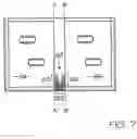
FIG. 7 is a plan view of the rear of a display assembly according to a further embodiment of the present invention in a compact configuration.
DETAILED DESCRIPTION OF THE PREFERRED EMBODIMENTIn order that members of the public may understand how the present invention may be put into practice a preferred embodiment of the invention will now be described.
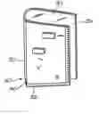
A schematic view of a typical prior art passive matrix display assembly 10 is shown in FIG. 1. The liquid crystal display 12 is designed to display dot pattern images. A plurality of row and column electrodes are horizontally and vertically disposed across the liquid crystal display. Connection points for the electrodes are located along edges of the liquid crystal display.
Circuit boards 14 and 18 are coupled to the row and column electrodes of the LCD by means of tape automated bonding (TAB) films 22 and 24. PCB's 14 and 18 support circuitry including a row driver chip and column driver chip, 26 and 28 respectively, for applying potentials to selected row and column electrodes in order to selectively activate liquid crystal cells to form a display. For mounting in an apparatus such as a laptop computer or mobile phone the printed circuit boards 18 and 14 may be folded back behind the screen as shown in FIG. 2 which is a rear view of the display assembly. It will be realized that flexing of the LCD 12 would place a strain on the TAB connections 22, 24 to each of PCBs 14 and 18.
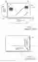
A preferred embodiment of the present invention will now be described with reference to FIG. 3. FIG. 3 depicts a flexible LCD screen 30 including TAB connections 32 and 34 for connecting to display row electrodes.
Beneath the lower edges of the flexible LCD 30 there are located two angled TAB strips 36 and 38. Connection points on each of the angled TAB strips are connected to column electrodes of the LCD display by means of flexible wire looms 40 and 42 respectively. It may be noted that in the presently described embodiment, the distance L1 along the TAB strip 36 is equal to the distance L1 along the column electrodes to which it is connected by wire loom 42. Accordingly the distance between the column electrodes is maintained as the distance between contacts on the TAB strip which may be desirable in some circumstances. The arrangement is identical in respect of the left hand TAB strip 38 which has a length L2=L1.
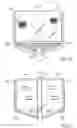
FIG. 4 shows a rear view of the display of FIG. 3 with PCBs 44 and 46 attached to the folded over TAB strips 32-38. It will be noted that there is sufficient width in the longitudinal region of the screen, defined by edges A-A′ and B-B′, of the PCBs for the display to be curved or folded on itself without creasing. The bottom edge 41 of screen 30 along with edge A-A′ of PCB 46 and TAB film 38 define a right triangle 39. Similarly triangle 37 is defined by edge B-B′ of PCB 44 and TAB film 36.
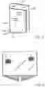
The display assembly is shown curved upon itself to a compact configuration in FIG. 5. Upon folding the screen as shown in FIG. 5 the wires connecting column electrode connection points in the region between lines A-A′ and B-B′ (FIG. 3) to TAB strips 36 and 38 tighten. Accordingly a degree of slack must be present in those wires of looms 40 and 42 when the assembly is in an open configuration as shown in FIG. 6.
Computational devices such as laptop computers, electronic books and the like may be designed with a hinged or otherwise folding housing to incorporate the display assembly thereby facilitating formation of a compact device. A further embodiment of the invention is depicted in FIG. 7. FIG. 7 shows the rear of a display assembly in which the PCBs 54 and 56 do not project from the bottom of the screen. Rather column electrode connection points 52 in the region between A-A′ and B-B′ are connected to connection points 60 and 62 on the inner edges of PCBs 54 and 56 by flexible connectors 58.
Variations of the invention other than the embodiments that have been described with reference to FIGS. 3-7 are of course possible. For example other types of flexible display screen may be used such as an organic light emitting diode screen. Furthermore, the connection between the electrode contacts and the angled TAB films 38, 36 (FIG. 4) might be made by means other than wire looms. For example a flexible film having conductive traces upon it might be used to make the connections. Although the preferred embodiment has two printed circuit board defining a longitudinal flexing region of the screen it would also be possible to construct embodiments of the invention with other numbers of circuit boards.
While a preferred embodiment of the present invention has been described in detail herein, it should be clearly understood that many variations and/or modifications of the basic inventive concepts herein taught, which may appear to those skilled in the present art will still fall within the spirit and scope of the present invention as defined in the appended claims.
Claims
1. A flexible display assembly including:
a flexible display screen having a plurality of connection points;
at least two printed circuit boards located at the rear of said screen and defining a longitudinal region of the screen therebetween; and
flexible connectors between connection points located in said region and each of the printed circuit boards;
wherein the flexible connectors are of sufficient length to accommodate closing of the assembly about the longitudinal region.
2. An assembly according to claim 1, wherein the flexible connectors comprise looms of wires.
3. An assembly according to claim 2, wherein the printed circuit boards connect to the looms of wires by means of tape automated bonding films.
4. An assembly according to claim 1, wherein an edge of the screen and edges of the PCBs define triangles and the flexible connectors terminate along edges of the triangles.
5. An assembly according to claim 4, wherein said edge of the screen and edges of the PCBs define right triangles with the flexible connectors terminating along hypotenuses of the triangles.
6. An assembly according to claim 5, wherein the PCB's are shaped so that the sum of the lengths of the hypotenuses is equal to said length of the display screen.
7. An assembly according to claim 1, wherein the flexible connectors terminate along edges of the printed circuit board defining the longitudinal region of the screen.
8. An assembly according to claim 6 or claim 7, wherein the screen comprises a flexible liquid crystal display.
9. An assembly according to claim 6 or claim 7, wherein the screen comprises an organic light emitting diode display.
10. A computational device including an assembly according to claim 1.
11. A computational device including an assembly according to claim 6 or claim 7.
Images & Drawings included:
Sources:
- United States Patent and Trademark Office - verify current appl. status at the USPTO↗
Similar patent applications:
- » 10773248
Compact display assembly - » 15589980
Structurally compact display assembly with pressure fit - » 20170287365
Structurally compact display assembly - » 20180025669
Structurally compact display assembly with pressure fit - » 20180297391
Structurally compact backlit display assembly - » 20200278545
Photo-sensing reflectors for compact display module assembly - » 20200346481
STRUCTURALLY COMPACT BACKLIT DISPLAY ASSEMBLY - » 20200280162
Photo-sensing reflectors for compact display module assembly comprising a reflective coating on a light receiving surface of a reflective photodiode - » 20210011296
Photo-sensing reflectors for compact display module assembly - » 20110176332
Backlight assembly and cover for a compact display apparatus
Recent applications in this class:
- » 20250291389 2025-09-18
SCROLLABLE DISPLAY APPARATUS AND DISPLAY SYSTEM - » 20250291388 2025-09-18
FOLDABLE DISPLAY DEVICE - » 20250291387 2025-09-18
DEVICE ARRAY SUBSTRATE AND DISPLAY DEVICE - » 20250291386 2025-09-18
DISPLAY DEVICE AND ELECTRONIC DEVICE INCLUDING THE SAME - » 20250284319 2025-09-11
ELECTRONIC DEVICE COMPRISING FLEXIBLE DISPLAY, AND METHOD FOR CONTROLLING SAME - » 20250284318 2025-09-11
PANEL SUBSTRATE AND METHOD OF MANUFACTURING DISPLAY MODULE USING THE SAME - » 20250278119 2025-09-04
DISPLAY PANEL AND ELECTRONIC DEVICE - » 20250271903 2025-08-28
DISPLAY DEVICE AND METHOD FOR PROVIDING THE SAME - » 20250271902 2025-08-28
FOLDABLE ELECTRONIC DEVICE INCLUDING BEZEL SAG PREVENTING STRUCTURE - » 20250271901 2025-08-28
ROLL-SLIDE DISPLAY DEVICE
Recent applications for this Assignee:
- » 20130176441 2013-07-11
User interface system employing printed substrate and substrate sensing device - » 20130176221 2013-07-11
SENSING DEVICE HAVING CURSOR AND HYPERLINKING MODES - » 20130100297 2013-04-25
Method of enabling association of object with surface - » 20130092732 2013-04-18
SYSTEM HAVING SENSING DEVICE FOR SENSING DATA ENCODED BY MARKS - » 20130090481 2013-04-11
Sulfonated dye salts exhibiting reduced kogation - » 20110279596 2011-11-17
PRINTING SYSTEM HAVING MULTI-PATH VALVE FOR GAS VENTING - » 20080123969 2008-05-29
Localized signal data preservation within signal bandwidth - » 20080117403 2008-05-22
Platen unit for a disposable camera having a printer - » 20070002121 2007-01-04
HANDHELD MOBILE COMMUNICATIONS DEVICE WITH A DETACHABLE PRINTING MECHANISM AND A SLOT FOR PRINT MEDIA - » 20060250475 2006-11-09
Image recordal and generation apparatus