Transformer level driving circuit
US20050174013A1
2005-08-11
11/100,556
2005-04-07
✅ Patent granted
US 7,279,822 B2
2007-10-09
-
-
Thomas M. Dougherty
2025-07-23
Abstract:
A transformer level driving circuit mainly aims to drive a medium voltage system. It includes a control unit to generate a resonant frequency and output phase signal waveforms, and a medium voltage driving circuit which includes a floating level unit and a driving unit which receives a medium voltage electric input. The driving unit actuates opening and closing at different time to enable the floating level unit to output a voltage floating level thereby to drive a ceramic transformer to control the medium voltage system through a low voltage level.
Inventors:
- Chin-Wen CHOU 89 🇹🇼 Taipei Hsien, Taiwan
- Kuang-Ming Wu 11 🇹🇼 Taipei Hsien, Taiwan
- Eddie Cheng 6 🇹🇼 Taipei Hsien, Taiwan
- K. M. Wu 2 🇹🇼 Taipei Hsien, Taiwan
- Chih-Chang Lin 2 🇹🇼 Taipei Hsien, Taiwan
Assignee:
- Zippy Technology Corp. 97 🇹🇼 Taipei Hsien, Taiwan
Interested in similar patents?
Get notified when new applications in this technology area are published.
Classification:
H01L41/044 » CPC main
Piezo-electric devices in general; Electrostrictive devices in general; Magnetostrictive devices in general; Processes or apparatus specially adapted for the manufacture or treatment thereof or of parts thereof; Details thereof; Details of piezo-electric or electrostrictive devices; Drive or control circuitry or methods for piezo-electric or electrostrictive devices not otherwise provided for for piezoelectric transformers
H05B41/2828 » CPC further
Circuit arrangements or apparatus for igniting or operating discharge lamps; Circuit arrangements in which the lamp is fed by power derived from dc by means of a converter, e.g. by high-voltage dc using static converters with semiconductor devices by means of a bridge converter in the final stage using control circuits for the switching elements
H02M3/158 » CPC further
Conversion of dc power input into dc power output without intermediate conversion into ac by static converters using discharge tubes with control electrode or semiconductor devices with control electrode using devices of a triode or transistor type requiring continuous application of a control signal using semiconductor devices only with automatic control of output voltage or current, e.g. switching regulators including plural semiconductor devices as final control devices for a single load
Y02B70/10 » CPC further
Technologies for an efficient end-user side electric power management and consumption Technologies improving the efficiency by using switched-mode power supplies [SMPS], i.e. efficient power electronics conversion e.g. power factor correction or reduction of losses in power supplies or efficient standby modes
H01L41/09 IPC
Piezo-electric devices in general; Electrostrictive devices in general; Magnetostrictive devices in general; Processes or apparatus specially adapted for the manufacture or treatment thereof or of parts thereof; Details thereof; Piezo-electric or electrostrictive devices with electrical input and mechanical output, e.g. actuators, vibrators
Description
This application is a continuation-in-part, and claims priority, of from U.S. patent application Ser. No. 10/745,592 filed on Dec. 29, 2003, entitled “Ceramic transformer level driving circuit”.
FIELD OF THE INVENTIONThe present invention relates to a transformer level driving circuit and particularly to a driving circuit to drive a medium voltage system.
BACKGROUND OF THE INVENTIONAt present the liquid crystal display (LCD) used in desktop and notebook computers, PDA and Webpad mostly employs a driving device to output high voltage, and through a ceramic transformer or a wired transformer to ignite a cold cathode fluorescent lamp (CCFL). The technique adopted by the conventional driving devices is discussed as follows:
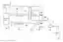
Referring to FIGS. 1A and 1B, an electric unit 14 delivers electricity to a control unit 10 and a driving unit 13. The control unit 10 outputs two positive phase signal waveforms 11 and 12 to control operations of the driving unit 13. The driving unit 13 is a push-pull amplifier consisting of a P-MOSFET 131 and a N-MOSFET 132. When the positive signal phase waveform 11 output from the control unit 10 reaches the P-MOSFET 131, the P-MOSFET 131 is located at the lower side of the positive phase signal waveform 11 and in a conductive state. Another positive phase signal waveform 12 reaches the N-MOSFET 132, the N-MOSFET 132 is located at the upper side of the positive phase signal waveform 12 and in a conductive state. Under the actuation of the P-MOSFET 131 and the N-MOSFET 132, the driving unit 13 outputs a medium voltage level to drive a driving inductor 15 and a ceramic transformer 16 to ignite a CCFL 17. The positive phase signal waveforms 11 and 12 have time difference, namely dead time 111 (as shown in FIG. 1B). The dead time 111 aims to prevent the P-MOSFET 131 and N-MOSFET 132 from being conductive at the same time and resulting in over short and burn out.
The P-MOSFET 131 has characteristics of electronic hole flow while the N-MOSFET 132 has characteristics of electron flow. The electron flow can generate energy three times as the electronic hole flow does. Hence using one N-MOSFET 132 is equivalent to using three P-MOSFETs 131. Therefore employing a high power to drive the ceramic transformer 16 and CCFL 17, the cost of P-MOSFET 131 is much greater. As a result, the driving circuit also is expensive.
SUMMARY OF THE INVENTIONTherefore the primary object of the present invention is to provide a transformer level driving circuit that uses a N-MOSFET to replace a P-MOSFET.
The transformer level driving circuit according to the invention includes a control unit and a medium voltage driving circuit. The control unit outputs two phase signal waveforms through a resonant frequency. The medium voltage driving circuit includes a floating level unit and a driving unit which receives a medium voltage electric input. The driving unit consists of two N-MOSFETs. The first N-MOSFET is controlled by the first phase signal to open and close. The second N-MOSFET is controlled by the second phase signal to open and close. The first and the second N-MOSFETs perform opening and closing operations at different time to enable the floating level unit to output a voltage floating level. The driving unit performs opening and closing operations at different time to enable the floating level unit to output a voltage floating level to drive the ceramic transformer, thereby a lower voltage level may be used to control a medium voltage system.
BRIEF DESCRIPTION OF THE DRAWINGSFIG. 1A is a block diagram of a conventional technique for driving a CCFL.
FIG. 1B is a schematic view of conventional driving waveforms.
FIG. 2A is a block diagram of the present invention.
FIG. 2B is a schematic view of driving waveforms according to the present invention.
FIG. 3 is a block diagram of an embodiment of the present invention.
FIG. 4 is a block diagram of another embodiment of the present invention.
FIG. 5 is a block diagram of yet another embodiment of the present invention.
DETAILED DESCRIPTION OF THE PREFERRED EMBODIMENTSThe foregoing, as well as additional objects, features and advantages of the invention will be more readily apparent from the following detailed description, which proceeds with reference to the accompanying drawings.
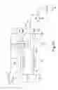
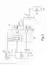
Please referring to FIGS. 2A and 2B, the transformer level driving circuit according to invention includes:
-
- a control unit 20 to receive low voltage electricity from an electric unit 25 and generate a resonant frequency and output a first phase signal waveform 21 and a second phase signal waveform 22 (being two positive phase signal waveforms);
- a waveform transformation unit 23 to provide an inverter 230 and a converter 231 for waveform phase transformation of the first phase signal waveform 21 and second phase signal waveform 22. The positive phase signal waveform 21 is transformed to a first phase signal 210 through the inverter 230 (as shown in FIG. 2B). Another positive phase signal waveform 22 is deferred to become a second phase signal 220 (as shown in FIG. 2B). The transformed first and second phase signals 210 and 220 lag behind the positive phase signal waveforms 21 and 22 slightly. Hence there is a time difference, i.e. a dead time 213, between the first phase signal 210 and the second phase signal 220 (referring to FIG. 2B); and
- a medium voltage driving circuit 24 which includes a floating level unit 240 and a driving unit 241 which receives a medium voltage electric input. The driving unit 241 consists of two N-MOSFETs 242 and 243. The first N-MOSFET 242 is controlled by the transformed first phase signal 210 to open and close. The second N-MOSFET 243 is controlled by the transformed second phase signal 220 to open and close. The first N-MOSFET 242 and second N-MOSFET 243 open and close at different time to enable the floating level unit 240 to output a voltage floating level at an output end 244 thereof to drive an inductor 26 and a ceramic transformer 27 thereby to ignite a CCFL 28. The dead time 213 aims to prevent the first N-MOSFET 242 and the second N-MOSFET 243 to become conductive at the same time and result in instantaneous over short and cause burn out. Thus the dead time 213 can serve as a buffer to prevent the first N-MOSFET 242 and the second N-MOSFET 243 from operating at the same time.
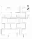
Refer to FIG. 3 for the first embodiment of the invention. The control unit 20 receives low voltage electricity from the electric unit 25 and generates a resonant frequency and outputs a positive phase signal waveform 21a and an inverse phase signal waveform 22a. The waveform transformation unit 23 includes two inverters 232 and 233 to perform transformation and deferring. While the positive phase signal waveform 21a is transformed to a first phase signal 211 through the first inverter 232, the inverse phase signal waveform 22a is transformed to a second phase signal 221 through another inverter 233 (the load driving process of the first and second phase signals 211 and 221 is same as previously discussed, thus details are omitted).
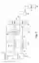
Second EmbodimentRefer to FIG. 4 for the second embodiment of the invention. The control unit 20 receives low voltage electricity from the electric unit 25 and generates a resonant frequency and outputs two inverse phase signal waveforms 21b and 22b. The waveform transformation unit 23 includes a converter 234 and an inverter 235 to perform transformation and deferring operations. While the inverse phase signal waveform 21b is transformed to a first phase signal 212 through the converter 234, another inverse phase signal waveform 22b is transformed to a second phase signal 222 through the inverter 235 (the load driving process of the first and second phase signals 212 and 222 is same as previously discussed, thus details are omitted).
Third EmbodimentRefer to FIG. 5 for yet another embodiment of the invention. The control unit 20 receives low voltage electricity from the electric unit 25 and generates a resonant frequency and outputs two phase signal waveforms 21c and 22c of opposite phases that have a time difference. No waveform transformation unit is needed. Namely, the first N-MOSFET 242 and the second N-MOSFET 243 are driven directly. The floating level unit 240 outputs a voltage floating level on an output end 244 thereof to drive the inductor 26 and the ceramic transformer 27 thereby to ignite the CCFL 28.
The embodiments previously discussed take the ceramic transformer 27 as an example. In fact, the invention can be adopted on wired transformers equally well. The circuit principle and effect are the same. Thus details are omitted.
While the preferred embodiments of the invention have been set forth for the purpose of disclosure, modifications of the disclosed embodiments of the invention as well as other embodiments thereof may occur to those skilled in the art. Accordingly, the appended claims are tended to cover all embodiments which do not depart from the spirit and scope of the invention.
Claims
1. A transformer level driving circuit, comprising:
a control unit for receiving low voltage electricity and outputting a first phase signal waveform and a second phase signal waveform; and
a medium voltage driving circuit including a floating level unit and a driving unit which receives medium voltage electric input, said driving unit consisting of two N-MOSFETs, said first N-MOSFET being controlled by a first phase signal for opening and closing, said second N-MOSFET being controlled by a second phase signal for opening and closing, said first N-MOSFET and said second N-MOSFET being opened and closed at different time such that said floating level unit outputs a voltage floating level.
2. The transformer level driving circuit according to claim 1, wherein said first phase signal waveform and said second phase signal waveform output by said control unit have opposite phases.
3. The transformer level driving circuit according to claim 2, wherein said first phase signal waveform and said second phase signal waveform have a time difference.
4. The transformer level driving circuit according to claim 1, wherein said first phase signal and said second phase signal are output by said control unit and go through waveform phase transformation through a waveform transformation unit.
5. The transformer level driving circuit according to claim 4, wherein the waveform transformation unit performs waveform phase transformation of the first phase signal waveform and the second phase signal waveform through a first phase converter and a second phase converter.
6. The transformer level driving circuit according to claim 5, wherein said first phase signal waveform and said second phase signal waveform are positive phase signal waveforms and said first phase converter and said second phase converter are an inverter and a converter.
7. The transformer level driving circuit according to claim 5, wherein said first phase signal waveform is a positive phase signal waveform and said second phase signal waveform is an inverse phase signal waveform, and said first phase converter and said second phase converter are two inverters.
8. The transformer level driving circuit according to claim 5, wherein said first phase signal waveform and said second phase signal waveform are inverse phase signal waveforms and said first phase converter and said second phase converter are is a converter and an inverter.
9. The transformer level driving circuit according to claim 5, wherein said first phase converter and said second phase converter perform waveform transformation simultaneously to form said first phase signal waveform and said second signal waveform that have a time difference.
Images & Drawings included:


Sources:
- United States Patent and Trademark Office - verify current appl. status at the USPTO↗
Similar patent applications:
- » 20050146245
Ceramic transformer level driving circuit
Recent applications in this class:
- » 20220123196 2022-04-21
Driver circuitry comprising active inductor circuitry for driving piezoelectric transducers - » 20210135086 2021-05-06
OUTPUT FILTER FOR POWER TRAIN - » 20200411745 2020-12-31
Device for producing a non-thermal atmospheric pressure plasma and method for operating a piezoelectric transformer - » 20200098968 2020-03-26
POWER CONVERTER - » 20190198746 2019-06-27
Control circuit and method for controlling a piezoelectric transformer - » 20190097119 2019-03-28
Piezoelectric transmitter - » 20180145242 2018-05-24
POWER SUPPLY CIRCUIT AND AC ADAPTOR - » 20170077384 2017-03-16
Drive signal generating apparatus - » 20160064640 2016-03-03
POWER SUPPLY DEVICE AND POWER SUPPLY METHOD - » 20160043298 2016-02-11
Frequency tracking piezoelectric transformer power converter with simultaneous two-parameter control
Recent applications for this Assignee:
- » 20120173898 2012-07-05
Remote controlled computer system that avoids accidental power cycling by selectively transmitting a manual trigger signal to a motherboard based on the presence of a power activating signal from a connected power supply - » 20120033450 2012-02-09
Multiple power supplies balance system - » 20120032820 2012-02-09
Luminous keyboard - » 20120018289 2012-01-26
Local lighting keyboard - » 20110168538 2011-07-14
Thin illuminated keyboard - » 20100110737 2010-05-06
Multi-output power supply - » 20100039297 2010-02-18
Keyboard with illuminating architecture - » 20090316450 2009-12-24
Power supply device with system switch circuit - » 20090284077 2009-11-19
Multi-input power-switching circuit - » 20090233460 2009-09-17
Output adapting device of plug-in power system