Thin film transistor array panel for display
US20050174846A1
2005-08-11
11/002,617
2004-12-03
✅ Patent granted
US 7,148,509 B2
2006-12-12
-
-
Ida M. Soward
2024-12-09
Abstract:
A TFT array panel is provided, including an insulating substrate, gate lines horizontally provided on the insulating substrate, data lines isolated from the gate lines and intersecting the gate lines, a pixel electrode in a pixel region defined by intersecting the gate lines and data lines, a TFT for transmitting or intercepting an image signal transmitted through the plurality of data lines to the pixel electrode in response to a scanning signal transmitted from the plurality of gate lines, a transmission gate for distributing the image signal input from an input line to the plurality of data lines, and a repair line intersecting the input line of the transmission gate. Therefore, since the input repair line and the input line of the transmission gate are intersected, a parasitic capacitance occurring between the repair line and the input line of the transmission gate can be reduced.
Inventors:
- Il Gon KIM 73 🇰🇷 Seoul, South Korea
- Tae-Hyeong PARK 25 🇰🇷 Yongin-si, South Korea
- Cheol-Min Kim 13 🇰🇷 Seongnam-si, South Korea
- Chul-Ho Kim 1 🇰🇷 Uijeongbu-si, South Korea
- Chul-Ho Kim 1 🇰🇷 Uiieongbu-si, South Korea
Assignee:
- Samsung Electronics Co., Ltd 16,186 🇰🇷 , South Korea
Interested in similar patents?
Get notified when new applications in this technology area are published.
Classification:
H01L29/04 IPC
Semiconductor devices adapted for rectifying, amplifying, oscillating or switching, or capacitors or resistors with at least one potential-jump barrier or surface barrier, e.g. PN junction depletion layer or carrier concentration layer; Details of semiconductor bodies or of electrodes thereof; Multistep manufacturing processes therefor; Semiconductor bodies ; Multistep manufacturing processes therefor characterised by their crystalline structure, e.g. polycrystalline, cubic or particular orientation of crystalline planes
H01L29/15 IPC
Semiconductor devices adapted for rectifying, amplifying, oscillating or switching, or capacitors or resistors with at least one potential-jump barrier or surface barrier, e.g. PN junction depletion layer or carrier concentration layer; Details of semiconductor bodies or of electrodes thereof; Multistep manufacturing processes therefor; Semiconductor bodies ; Multistep manufacturing processes therefor characterised by the materials of which they are formed Structures with periodic or quasi periodic potential variation, e.g. multiple quantum wells, superlattices
H01L31/036 IPC
Semiconductor devices sensitive to infra-red radiation, light, electromagnetic radiation of shorter wavelength or corpuscular radiation and specially adapted either for the conversion of the energy of such radiation into electrical energy or for the control of electrical energy by such radiation; Processes or apparatus specially adapted for the manufacture or treatment thereof or of parts thereof; Details thereof characterised by their semiconductor bodies characterised by their crystalline structure or particular orientation of the crystalline planes
H01L29/10 IPC
Semiconductor devices adapted for rectifying, amplifying, oscillating or switching, or capacitors or resistors with at least one potential-jump barrier or surface barrier, e.g. PN junction depletion layer or carrier concentration layer; Details of semiconductor bodies or of electrodes thereof; Multistep manufacturing processes therefor; Semiconductor bodies ; Multistep manufacturing processes therefor characterised by their shape; characterised by the shapes, relative sizes, or dispositions of the semiconductor regions ; characterised by the concentration or distribution of impurities within semiconductor regions with semiconductor regions connected to an electrode not carrying current to be rectified, amplified or switched and such electrode being part of a semiconductor device which comprises three or more electrodes
H01L31/113 IPC
Semiconductor devices sensitive to infra-red radiation, light, electromagnetic radiation of shorter wavelength or corpuscular radiation and specially adapted either for the conversion of the energy of such radiation into electrical energy or for the control of electrical energy by such radiation; Processes or apparatus specially adapted for the manufacture or treatment thereof or of parts thereof; Details thereof in which radiation controls flow of current through the device, e.g. photoresistors characterised by at least one potential-jump barrier or surface barrier, e.g. phototransistors; Devices sensitive to infra-red, visible or ultra-violet radiation characterised by field-effect operation, e.g. junction field-effect phototransistor being of the conductor-insulator-semiconductor type, e.g. metal-insulator-semiconductor field-effect transistor
G02F1/1345 » CPC main
Devices or arrangements for the control of the intensity, colour, phase, polarisation or direction of light arriving from an independent light source, e.g. switching, gating or modulating; Non-linear optics for the control of the intensity, phase, polarisation or colour based on liquid crystals, e.g. single liquid crystal display cells; Constructional arrangements; Operation of liquid crystal cells; Circuit arrangements; Constructional arrangements; Manufacturing methods Conductors connecting electrodes to cell terminals
G02F1/136259 » CPC further
Devices or arrangements for the control of the intensity, colour, phase, polarisation or direction of light arriving from an independent light source, e.g. switching, gating or modulating; Non-linear optics for the control of the intensity, phase, polarisation or colour based on liquid crystals, e.g. single liquid crystal display cells; Constructional arrangements; Operation of liquid crystal cells; Circuit arrangements; Liquid crystal cells structurally associated with a semi-conducting layer or substrate, e.g. cells forming part of an integrated circuit; Active matrix addressed cells Repairing; Defects
H01L27/12 » CPC further
Devices consisting of a plurality of semiconductor or other solid-state components formed in or on a common substrate including semiconductor components specially adapted for rectifying, oscillating, amplifying or switching and having at least one potential-jump barrier or surface barrier; including integrated passive circuit elements with at least one potential-jump barrier or surface barrier the substrate being other than a semiconductor body, e.g. an insulating body
Description
BACKGROUND OF THE INVENTION(a) Field of the Invention
The present invention relates to a thin film transistor array panel for a display.
(b) Description of the Related Art
A thin film transistor (TFT) array panel includes gate lines horizontally disposed on an insulating substrate, an gate insulating layer on the gate lines, a semiconductor pattern on the gate insulating layer located over a gate electrode of the gate line, contact layers spaced apart from each other centering the gate lines on the semiconductor pattern, and data lines vertically disposed on the gate insulating layer. In the data lines, a source electrode extends to the upper portion of one end of the contact layer in a branch-shape, and a drain electrode is provided on the other portion of the contact layer and connected to a pixel electrode. Generally, the pixel electrode is provided on a protection layer covering the drain electrode and the data line, etc., and connected to the drain electrode through a contact hole formed in the protection layer.
In the TFT array panel, repair lines are provided in the vicinity of active regions where the gate line and the data line are intersected, to prevent a malfunction that may occur due to disconnection of the data line or a short-circuit between the gate line and the data line. For example, when a gate line and data line are short-circuited, it can be repaired by connecting both ends of the short-circuited data line to the repair line and disconnecting both ends of the short-circuited data line using a laser beam. However, the method using the repair lines can bring a problem of resistance capacitance (RC) delay according to increase of LCD size.
SUMMARY OF THE INVENTIONThe technical objective of the present invention is to resolve RC delay of the repair line in a TFT array panel for a display.
To achieve the objective, the present invention provides a TFT array panel for a display having a repair line in an input terminal of a transmission gate.
In detail, the present invention provides a TFT array panel comprising: an insulating substrate; gate lines horizontally provided on the insulating substrate; data lines isolated from the gate line and intersecting the gate lines; a pixel electrode in a pixel region defined by intersecting the gate lines and data lines; a TFT for transmitting or intercepting an image signal transmitted through the plurality of data lines to the pixel electrode in response to a scanning signal transmitted from the plurality of gate lines; a transmission gate for distributing the image signal input from an input line to the plurality of data lines; and a repair line intersecting the input line of the transmission gate.
In the structure, it is preferable that the repair line is divided with an input terminal repair line and an end repair line, and that a repair transmission gate is further included in the TFT array panel to connect the input repair line with the end repair line. The transmission gate includes a plurality of TFTs having each output terminal connected to each data line, each input terminal connected to the transmission gate input line, and each gate terminal connected to the scanning signal lines of the transmission gate. The repair transmission gate may include an output terminal connected to the end repair line, an input terminal connected to the input repair line, and a gate terminal overlapped with gate terminal connecting pieces connected to the transmission gate scanning signal lines. Here, three input terminals of the transmission gate form a set and are connected to the input line of the transmission gate. There are three transmission gate scanning signal lines, and they may be connected to three gate terminals of the transmission gate, respectively, corresponding to a set of the input terminals. There are three gate terminal connecting pieces overlapped with the gate terminals of the repair transmission gate and they can be connected to three transmission gate scanning signal lines, respectively. In addition, diodes may be further included to connect the input line of the transmission gate and the input terminal of the repair transmission gate with a power supply line. Also, the length of channels of the repair transmission gate is longer than that of the channels of the transmission gate.
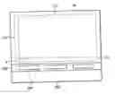
BRIEF DESCRIPTION OF THE DRAWINGSFIG. 1 is a plane diagram of a thin film transistor array panel according to an embodiment of the present invention.
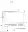
FIG. 2 is a diagram enlarging a portion of “A” in FIG. 1.
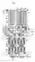
FIG. 3 is a cross-sectional view cut along III-III′ in FIG. 1
FIG. 4 is a cross-sectional view cut along IV-IV′ in FIG. 1
FIG. 5 is a cross-sectional view cut along V-V′ in FIG. 1.
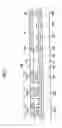
FIG. 6 is a circuit diagram of a thin film transistor array panel according to an embodiment of the present invention.
DETAILED DESCRIPTION OF THE PREFERRED EMBODIMENTSHereinafter, a preferred embodiment of the present invention will be described with reference to the accompanying drawings.
In the drawings, the thickness of several layers and regions are enlarged to show them more clearly, and similar elements have the same reference numbers throughout the specification. In addition, the expression that a layer, region, board, or panel is “on” something may mean the case when it is not only directly on something, but that something else may be provided therebetween. In addition, the expression that something is “under” something means there is nothing interposed therebetween.
The TFT array panel of the present invention can be applied to LCDs, OLEDs, etc. However, the embodiment of the present invention will be described defining a LCD.
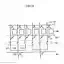
FIG. 1 is a plane diagram of a thin film transistor array panel according to an embodiment of the present invention, and FIG. 2 is a diagram enlarging a portion of “A” in FIG. 1.
A TFT array panel of the embodiment of the present invention comprises upper and lower display panels, and liquid crystal injected between the two panels.
FIG. 1 shows only a connection state of the lower display panel and a driving circuit unit, to allow the essential points of the present invention to be made clearly.
On an insulating layer 110, gate lines and data lines (not shown) are intersected, and a display region 112 having a TFT and a pixel electrode is provided. A gate line driving part 113 is provided on the left of the display region 112, and a transmission gate part 114, which is a portion of the data line driving circuit part, is provided on the lower portion of the display region 112. A flexible circuit board 510 having driving chips 540 thereon is provided on the lower portion of the insulating substrate 110, and a printed circuit board 550 is provided on the lower portion of the flexible circuit board 510. Accordingly, the flexible circuit board 510 connects the insulating substrate 110 with the printed circuit board 550.
Referring to FIG. 2, TFTs, of which output terminals are connected to the data lines 171, are provided to individually correspond to the data lines 171. Three input terminals 311, 312, and 313 of the TFT become a set and are connected to an input line 310 of the transmission gate. Three gate terminals 432, 442, and 452 of the TFT are connected to the first, second, and third transmission gate scanning lines 430, 440, and 450, respectively. The transmission gate distributes the image signals from the input line 310 of the transmission gate to three data lines 171 in response to the transmission gate scanning signals.
The input line 310 of the transmission gate intersects a Vdd line 420 and a Vss line 410 as power supply lines. Two kinds of diodes are provided between the Vdd line 420 and the Vss line 410: one allows a current flows from the Vdd line 420 to the input line 310 of the transmission gate; and the other allows a current flows from the input line 310 of the transmission gate to the Vss line 410. These diodes either disperse static electricity coming in from the display panel to the entire display panel or emit it to the outside.
An input repair line 401 is provided outside the Vss line 410, and it intersects the input line 310 of the transmission gate. Thus, when a repair is required, the input repair line 401 and the input line 310 of the transmission gate can be short-circuited by irradiating a laser beam to the intersection of the input repair line 401 and the input line 310 of the transmission gate.
A repair transmission gate is provided on the left of the leftmost transmission gate, and includes a TFT having a remarkably long channel. This TFT channel is about two times as long as the TFT channel of a common transmission gate. Accordingly, resistance of this TFT becomes about half of that of the TFT of the common transmission gate.
In the repair transmission gate, an input terminal line 320 is connected to the input repair line 401, and an output terminal line 330 is connected to an end repair line 402. The end repair line 402 is provided to intersect the end portions of the data lines 171, detouring around the display region 112. Gate terminals 461 and 462 are connected to a gate terminal line 460.
The gate terminal line 460 of the repair transmission gate is overlapped with all of the first, second, and third gate terminal connecting pieces 433, 443, and 453 connected to the first, second, and third transmission gate scanning lines 430, 440, and 450, respectively. This structure is to short-circuit the gate terminal line 460 and one of the gate terminal connecting pieces 433, 443, and 453 by irradiating a laser beam thereto, in repairing the data line 171 using the repair lines 401 and 402. Thus, the repair transmission gate operates by being synchronized with the corresponding transmission gate scanning signal.
The input terminal line 320 of the repair transmission gate is connected to the Vdd line 420 and Vss line 410 through two kinds of diodes. One of the diodes allows a current flows from the Vdd line 420 to the input terminal line 320 of the repair transmission gate, and the other allows a current flows from the input terminal line 320 to the Vss line 410. These diodes either disperse static electricity coming in from the display panel to the entire display panel, or emit it to the outside.
Hereinafter, a structure of the transmission gate 114 will be described in more detail with reference to the figures.
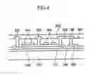
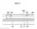
FIG. 3 is a cross-sectional view cut along II-II′ in FIG. 1, FIG. 4 is a cross-sectional view cut along IV-IV′ in FIG. 1, and FIG. 5 is a cross-sectional view cut along V-V′ in FIG. 1.
A buffer layer 111 is provided on the insulating layer 110. Polycrystalline silicon layers 501, 502, 503, 504, 505, and 506 are provided on the buffer layer 111 to form channels of TFTs and diodes. A gate insulating layer 140 is provided on the polycrystalline silicon layers 501 to 506. In this structure, the polycrystalline silicon layers 501 to 506 include n-type or p-type impurities doped on the source and drain regions, and impurity-undoped channel regions.
On the gate insulating layer 140, there are provided gate lines (not shown) in the display region, the gate terminals 432, 442, and 452 of the TFTs, the first, second, and third transmission gate scanning lines 430, 440, and 450, the Vdd line 420, the Vss line 410, the repair lines 401 and 402, the gate terminal line 460 of the repair transmission gate, gate electrodes 421 and 422 of the diodes, and a first interlayer-insulating layer 801.
On the first interlayer-insulating layer 801, there are provided the data lines 171, the input terminals 311, 312, and 313 of the TFT, the input line 310 of the transmission gate, the first, second, and third gate terminal connecting pieces 431, 441, and 451 of the transmission gate, the output terminal line 330 of the repair transmission gate, the input terminal line 320 of the repair transmission gate, the first, second, and third gate terminal connecting pieces 433, 443, and 453 of the repair transmission gate and the source electrode 322 and the drain electrode 321 of the diode.
The data lines 171 are connected to the drain regions of the polycrystalline silicon layers 501, 502, and 503 through contact holes, and the input terminals 311, 312, and 313 of the TFT are connected to the source regions of the polycrystalline silicon layers 501, 502, and 503 through contact holes.
The first, second, and third gate terminal connecting pieces 431, 441, and 451 of the transmission gate are connected to the gate terminals 432, 442, and 452 of the TFT and the first, second, and third transmission gate scanning lines 430, 440, and 450 through the contact holes 141 to 146, to electrically connect the gate terminals 432, 442, and 452 with the first, second, and third transmission gate scanning lines 430, 440, and 450.
The output terminal line 330 of the repair transmission gate is connected to the drain region of the polycrystalline silicon layer 504 through a contact hole, and the input terminal line 320 of the repair transmission gate is connected to the source region of the polycrystalline silicon layer 504 through a contact hole. The first, second, and third gate terminal connecting pieces 433, 443, and 453 are connected to the first, second, and third transmission gate scanning lines 430, 440, and 450 through contact holes 186, 187, and 188. The output terminal line 330 of the repair transmission gate is connected to the end repair line 402 through a contact hole 149, and the input terminal line 320 of the repair transmission gate is connected to the input repair line 401 through a contact hole 148.
A source electrode 322 of a first diode is connected to the Vdd line 420 and the source region of the polycrystalline silicon layer 505. A drain electrode 321 of a second diode is connected to the Vss line 410 and the drain region of the polycrystalline silicon layer 506. The input terminal line 320 of the repair transmission gate is connected to the drain region of the polycrystalline silicon layer 505 and the source region of the polycrystalline silicon layer 506 through the contact holes, while being connected to a gate electrode 421 of the second diode through a contact hole 183.
When the gate lines or data lines are disconnected in the TFT array panel having the above structure, such trouble can be solved with the following method.
For example, in the case when the data line 171 is disconnected, a laser beam is irradiate to short-circuit the disconnected data line 171 and the end repair line 402, and to short-circuit the input repair line 401 and the input line 310 of the transmission gate connected to the disconnected data line 171. Also, a laser beam is irradiated to short-circuit the gate terminal line 460 of the repair transmission gate and one of the first, second, and third gate terminal connecting pieces 433, 443, and 453 connected to the transmission gate scanning lines 430, 440, and 450 corresponding to the disconnected data line 171.
As a result, the image signals intending to be applied to the disconnected data line 171 are applied to the disconnected data line 171 through the repair lines 401 and 402.
FIG. 6 is a circuit diagram of a thin film transistor array panel according to an embodiment of the present invention.
As shown in FIG. 6, in the TFT array panel of the present invention, the input repair line 401 is arrayed to intersect the input line 310 of the transmission gate, and thus a parasitic capacitance occurring between the input repair line 401 and input line 310 of the transmission gate is reduced. In the conventional TFT array, since a repair line 401′ is provided in the output terminal of the transmission gate to intersect all data lines, a parasitic capacitance at the input repair line 401′ is remarkably large. However, in the TFT array panel of the present invention, since the input repair line and the input line 310 of the transmission gate are intersected, the number of intersected wires is reduced by about a third, and thus the parasitic capacitance at the input repair line 401 is also reduced by about a third.
As mentioned above, the present invention can reduce the parasitic capacitance at the repair line by intersecting the input repair line and the input line of the transmission gate.
The present invention should not be considered to be limited to the particular examples described above, but rather should be understood to cover all aspects of the invention as fairly set out in the attached claims. Various modifications, equivalent processes, as well as numerous structures to which the may be applicable will be readily apparent to those of skill in the art to which the present invention is directed upon review of the instant specification.
Claims
1. A thin film transistor (TFT) array panel comprising:
an insulating substrate;
a plurality of gate lines horizontally provided on the insulating substrate;
a plurality of data lines isolated from the gate line and intersecting the plurality of gate lines;
a plurality of pixel electrodes in pixel regions defined by intersecting the plurality of gate lines and the plurality of data lines;
a plurality of TFT for transmitting or intercepting an image signal transmitted through the plurality of data lines to the pixel electrodes in response to a scanning signal transmitted from the plurality of gate lines;
a transmission gate for distributing the image signal input from an input line to the plurality of data lines; and
a repair line intersecting the input line of the transmission gate.
2. The TFT array panel of claim 1, wherein the repair line includes an input repair line and an end repair line, and the TFT array panel further comprises a repair transmission gate for connecting the input repair line to the end repair line.
3. The TFT array panel of claim 2, wherein the transmission gate includes a plurality of TFTs having each output terminal connected to each data line, each input terminal connected to an input line of the transmission gate, and each gate terminal connected to each scanning signal line of the transmission gate; and
the repair transmission gate has an output terminal connected to the end repair line, an input terminal connected to the input repair line, and gate terminals overlapped with gate terminal connecting pieces connected to the transmission gate scanning signal lines.
4. The TFT array panel of claim 3, wherein the transmission gate has three input terminals which form a set and are connected to the input line of the transmission gate;
the transmission gate scanning signal lines has three lines; and
the transmission gate has three gate terminals corresponding to the three input terminals of the transmission gate, and they are connected to the three transmission gate scanning signal lines, respectively.
5. The TFT array panel of claim 4, wherein the number of gate terminal connecting pieces overlapped with the gate terminals of the repair transmission gate is three, and three gate terminal connecting pieces are connected to three transmission gate scanning signal lines, respectively.
6. The TFT array panel of claim 3, further comprising diodes for connecting the input line of the transmission gate and the input terminal of the repair transmission gate to a power supply line.
7. The TFT array panel of claim 2, wherein the length of a channel of the repair transmission gate is longer than that of a channel of the transmission gate.
Images & Drawings included:
Sources:
- United States Patent and Trademark Office - verify current appl. status at the USPTO↗
Similar patent applications:
- » 20050067943
Thin film transistor array, display panel, method for inspecting the thin film transistor array, and method for manufacturing active matrix organic light emitting diode panel - » 20070171336
Color filter display panel, thin film transistor array panel, liquid crystal display thereof, and method thereof - » 20130082270
Thin-film transistor array device, EL display panel, EL display device, thin-film transistor array device manufacturing method, EL display panel manufacturing method - » 20120074421
Thin-film transistor array device, el display panel, el display device, thin-film transistor array device manufacturing method, el display panel manufacturing method - » 20120074422
Thin-film transistor array device, el display panel, el display device, thin-film transistor array device manufacturing method, el display panel manufacturing method - » 10147345
Liquid crystal display, thin film transistor array panel for liquid crystal display and manufacturing method thereof - » 20100195026
Display panel, thin film transistor array panel, and method for repairing display panel - » 20150092132
THIN FILM TRANSISTOR ARRAY PANEL, LIQUID CRYSTAL DISPLAY AND MANUFACTURING METHOD OF THIN FILM TRANSISTOR ARRAY PANEL - » 20130309821
Thin film transistor array substrate for a display panel and a method for manufacturing a thin film transistor array substrate for a display panel - » 20100308333
Thin film transistor array substrate for a display panel and a method for manufacturing a thin film transistor array substrate for a display panel
Recent applications in this class:
- » 20250123522 2025-04-17
GEOMETRIES FOR MITIGATING ARTIFACTS IN SEE-THROUGH PIXEL ARRAYS - » 20250085595 2025-03-13
LIQUID CRYSTAL DEVICE - » 20250020961 2025-01-16
DISPLAY PANELS AND MANUFACTURING METHODS THEREOF, DISPLAY DEVICES AND SPLICED DISPLAY DEVICES - » 20240361648 2024-10-31
LIGHT ADJUSTMENT DEVICE - » 20240361647 2024-10-31
FUNCTIONAL-LAYER BLANK AND METHOD FOR CONTACTING A FUNCTIONAL-LAYER BLANK - » 20240310681 2024-09-19
ELECTRO-OPTICAL DEVICE AND ELECTRONIC APPARATUS - » 20240192553 2024-06-13
ARRAY SUBSTRATE, LIQUID CRYSTAL DISPLAY PANEL AND LIQUID CRYSTAL DISPLAY APPARATUS - » 20240103324 2024-03-28
Electrooptical device and illumination device - » 20240045284 2024-02-08
Display device and method for manufacturing same - » 20240027852 2024-01-25
Display panels and manufacturing methods thereof, display devices and spliced display devices
Recent applications for this Assignee:
- » 20250175180 2025-05-29
INPUT BUFFER CIRCUIT AND POWER MANAGEMENT INTEGRATED CIRCUIT INCLUDING THE SAME - » 20250125998 2025-04-17
HYBRID SOURCE-SERIES TERMINATION DRIVER WITH CONSTANT OUTPUT SWING - » 20250117337 2025-04-10
PRE-FETCHING ADDRESS TRANSLATION FOR COMPUTATION OFFLOADING - » 20250069538 2025-02-27
DISPLAY DEVICE AND DRIVING METHOD THEREOF - » 20240430140 2024-12-26
RECEIVERS AND SEMICONDUCTOR MEMORY DEVICES INCLUDING THE SAME - » 20240414035 2024-12-12
RECEIVER, OPERATION METHOD THEREOF, AND MEMORY DEVICE - » 20240380824 2024-11-14
METHODS AND SYSTEMS TO PUSH NOTIFICATION MESSAGES IN SEAL NOTIFICATION MANAGEMENT SERVICE - » 20240377988 2024-11-14
MEMORY DEVICE AND OPERATION METHOD THEREOF - » 20240371417 2024-11-07
Semiconductor memory devices - » 20240348366 2024-10-17
METHOD AND APPARATUS FOR DECODING POLARIZATION-ADJUSTED CONVOLUTIONAL CODE BY USING LIST VITERBI ALGORITHM ADJUSTING LIST SIZE DYNAMICALLY